

SEMICONDUCTOR TECHNICAL DATA
Order this document
by MC145162/D
* ! * !($%
$"$ '
$#'!) )!&%*$%
CMOS
The MC145162 is a dual phase–locked loop (PLL) frequency synthesizer
especially designed for CT–1 cordless phone applications worldwide. This
frequency synthesizer is also for any product with a frequency operation at
60 MHz or below.
The MC145162–1 is a high frequency derivative of the MC145162, for
products with operating frequencies of 85 MHz or below.
The device features fully programmable receive, transmit, reference, and
auxiliary reference counters accessed through an MCU serial interface. This
feature allows this device to operate in any CT–1 cordless phone application.
The device consists of two independent phase detectors for transmit and
receive loops. A common reference oscillator, driving two independent
reference frequency counters, provides independent reference frequencies for
transmit and receive loops. The auxiliary reference counter allows the user to
select an additional reference frequency for receive and transmit loops if
required.
• Operating Voltage Range: 2.5 to 5.5 V
• Operating Temperature Range: – 40 to +
• Operating Power Consumption: 3.0 mA @ 2.5 V
• Maximum Operating Frequency:
MC145162 — 60 MHz @ 200 mV p–p, VDD = 2.5 V
MC145162–1 — 85 MHz @ 250 mV p–p, VDD = 2.5 V
• Three or Four Pins Used for Serial MCU Interface
• Built–In MCU Clock Output with Frequency of Reference Oscillator 3/4
• Power Saving Mode Controlled by MCU
• Lock Detect Signal
• On–Chip Reference Oscillator Supports External Crystals to 16.0 MHz
• Reference Frequency Counter Division Range: 16 to 4095
• Auxiliary Reference Frequency Counter Division Range: 16 to 16,383
• Transmit Counter Division Range: 16 to 65,535
• Receive Counter Division Range: 16 to 65,535
75°C
P SUFFIX
PLASTIC DIP
16
1
16
1
ORDERING INFORMATION
MC145162P Plastic DIP
MC145162D SOG Package
MC145162P1 Plastic DIP
MC145162D1 SOG Package
PIN ASSIGNMENT
1
CLK
2
AD
in
3
D
in
ENB
4
MCUCLK
V
6
SS
out
7
in
8
OSC
OSC
CASE 648
D SUFFIX
SOG PACKAGE
CASE 751B
16
LD
15
TxPD
14
fin–T
13
TxPS/f
125
V
DD
11
RxPS/F
10
RxPD
9
fin–R
out
Tx
Rx
out
REV 3.1
2/98
Motorola, Inc. 1998
MC145162•MC145162–1MOTOROLA
1
OSC
OSC
out
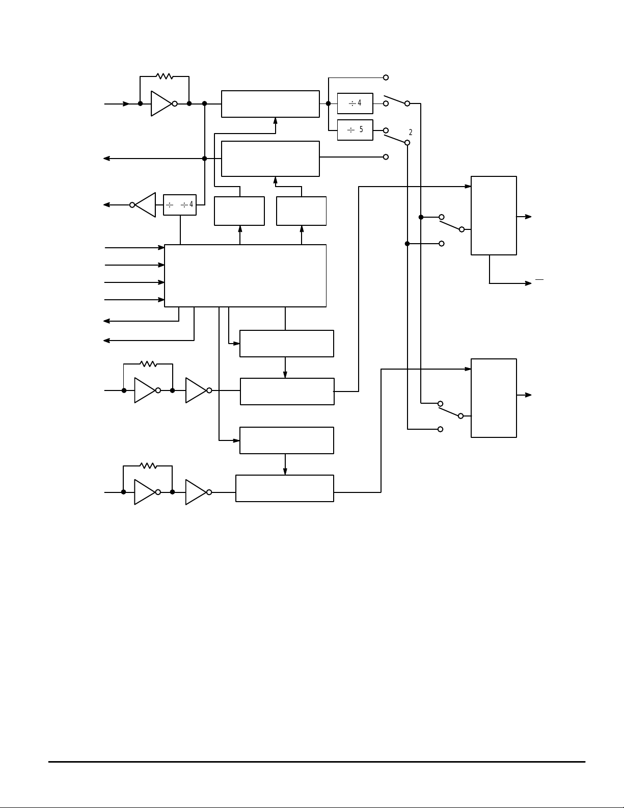
BLOCK DIAGRAM
A
f
R1
7
in
8
12–BIT PROGRAMMABLE
REFERENCE COUNTER
14–BIT PROGRAMMABLE
AUXILIARY REFERENCE
COUNTER
B
4
C
25
f
R2
D
MCUCLK
AD
in
CLK
D
in
ENB
TxPS/f
Tx
RxPS/f
Rx
fin–T
fin–R
5
2
1
3
4
13
11
14
9
3/
4
12–BIT SHIFT
REGISTER
MCU INTERFACE PROGRAMMING
MODE CONTROL
CONTROL REGISTER
16–BIT SHIFT REGISTER
16–BIT Tx PROGRAMMABLE
16–BIT SHIFT REGISTER
16–BIT Rx PROGRAMMABLE
14–BIT SHIFT
REGISTER
COUNTER
COUNTER
TRANSMIT
SELECT
RECEIVE
SELECT
VDD = PIN 12
VSS = PIN 6
Tx
PHASE
DETECTOR
Rx
PHASE
DETECTOR
15
16
10
TxPD
LD
RxPD
out
out
MC145162•MC145162–1 MOTOROLA
2
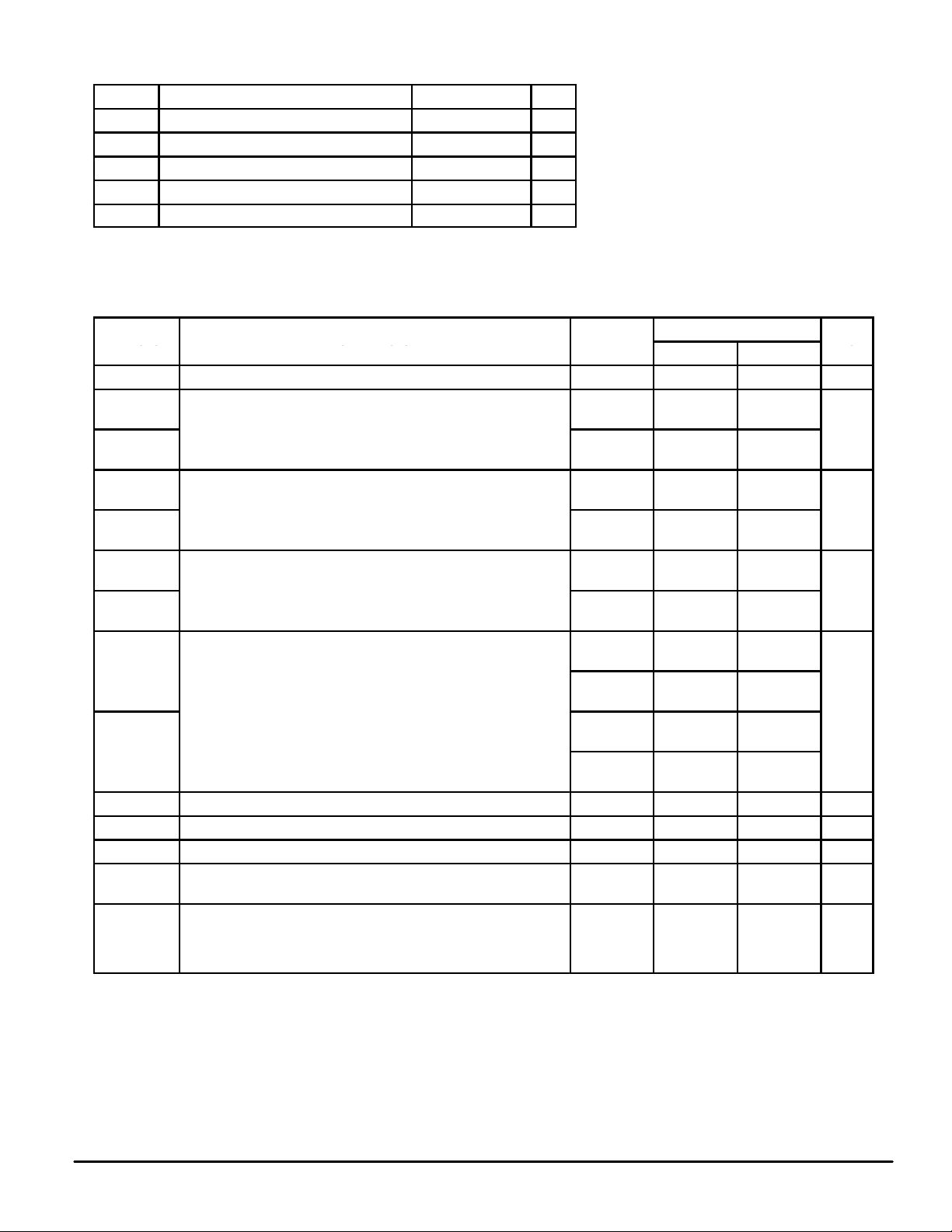
MAXIMUM RATINGS* (Voltages Referenced to V
Symbol Rating Value Unit
V
V
Iin, I
IDD, I
T
*Maximum Ratings are those values beyond which damage to the device may occur.
Functional operation should be restricted to the limits in the Electrical Characteristics
tables or Pin Descriptions section.
DC Supply Voltage – 0.5 to + 6.0 V
DD
Input Voltage, All Inputs – 0.5 to VDD + 0.5 V
in
DC Current Drain Per Pin 10 mA
out
DC Current Drain VDD or VSS Pins 30 mA
SS
Storage Temperature Range – 65 to + 150 °C
stg
SS
)
This device contains protection circuitry to
guard against damage due to high static voltages or electric fields. However, precautions
must be taken to avoid application of any voltage
higher than maximum rated voltages to this
high–impedance circuit. For proper operation,
Vin and V
VSS ≤ (Vin or V
Unused pins must always be tied to an
appropriate logic voltage level (e.g., either V
or VDD). Unused outputs must be left open.
should be constrained to the range
out
) ≤ VDD.
out
SS
ELECTRICAL CHARACTERISTICS (Voltages Referenced to V
Symbol Characteristic V
V
DD
V
OL
V
OH
V
IL
V
IH
I
OH
I
OL
I
IL
I
IH
I
OZ
C
in
C
out
I
DD(stdby)
I
DD
Power Supply Voltage Range — 2.5 5.5 V
Output Voltage 0 Level
(I
=0)
out
(Vin=VDD or 0) 1 Level 2.5
Input Voltage 0 Level
(V
= 0.5 V or VDD– 0.5 V)
out
Output Current (V
Input Current OSCin, fin–T, fin–R
(Vin=0)
(Vin=VDD– 0.5) OSCin, fin–T, fin–R 2.5
Three–State Leakage Current (V
Input Capacitance — — 8.0 pF
Output Capacitance — — 8.0 pF
Standby Current
(All Counters are in Power–Down Mode with Oscillator On)
Operating Current
MC145162: 200 mV p–p input at fin–T and fin–R = 60 MHz
MC145162–1: 250 mV p–p input at fin–T and fin–R = 85 MHz
with OSC = 10.24 MHz
= 2.2 V) Source
out
(V
= 5.0 V)
out
(V
= 0.3 V) Sink
out
(V
= 0.5 V)
out
= 0 V or 5.5 V) 5.5 — ± 100 nA
out
, TA = 25°C)
SS
1 Level 2.5
ADin, CLK, Din, ENB 2.5
ADin, CLK, Din, ENB 2.5
DD
2.5
5.5
5.5
2.5
5.5
5.5
2.5
5.5
2.5
5.5
2.5
5.5
5.5
5.5
5.5
2.5
5.5
2.5
5.5
Guaranteed Limit
Min Max
—
—
2.45
5.45
—
—
1.75
3.85
– 0.18
– 0.55
0.18
0.55
—
—
—
—
—
—
—
—
—
—
—
—
– 1.0
– 1.0
0.1
0.1
—
—
0.75
1.65
—
—
—
—
—
—
– 30
– 66
30
66
5.0
5.0
0.3
1.5
3.0
10
Unit
V
V
mA
µA
mA
mA
MC145162•MC145162–1MOTOROLA
3
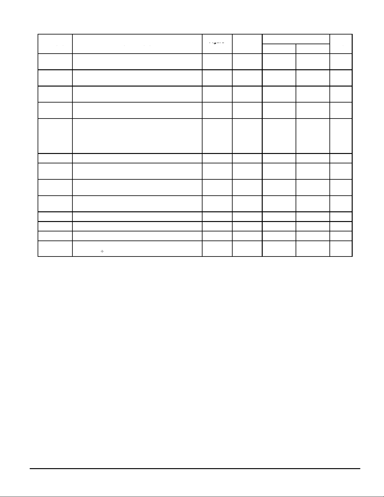
SWITCHING CHARACTERISTICS (T
Figure
Symbol Characteristic
t
TLH
t
THL
tr, t
t
w
f
max
t
st
t
su
t
h
t
rec
t
su1
t
h1
f Phase Detector Frequency dc 12.5 kHz
f
MCUCLK
Output Rise Time 1 2.5
Output Fall Time 1 2.5
Input Rise and Fall Time OSC
f
Input Pulse Width CLK and ENB 3 2.5
Input Frequency OSC
Input = Sine Wave @ ≥ 200 mV p–p fin–R, fin–T
for MC145162
Input = Sine Wave @ ≥ 250 mV p–p fin–R, fin–T
for MC145162–1
Minimum Start–Up Time 10 ms
Setup Time DATA to CLK
Hold Time CLK to DATA 5 3.0
Recovery Time ENB to CLK 5 3.0
Setup Time ENB to CLK 4 2.5 – 5.5 80 — ns
Hold Time CLK to ENB 4 2.5 – 5.5 600 — ns
Output Clock Frequency MCUCLK
(OSCin B 3)
= 25°C, CL = 50 pF)
A
ENB to CLK
Figure
No.
in
in
2 2.5
5 2.5
V
DD
5.5
5.5
5.5
5.5
2.5 – 5.5
2.5 – 5.5
2.5 – 5.5
5.5
5.0
5.0
Guaranteed Limit
Min Max
—
—
—
—
—
—
80
60
—
—
—
100
200
80
40
80
40
dc 5.33 MHz
200
100
200
100
5.0
4.0
—
—
16
60
85
—
—
—
—
—
—
Unit
ns
ns
µs
ns
MHz
ns
ns
ns
MC145162•MC145162–1 MOTOROLA
4
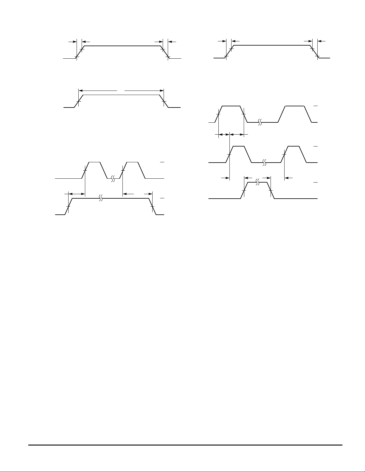
SWITCHING WAVEFORMS
ANY
OUTPUT
ENB, CLK
CLK
ENB
t
su1
t
TLH
10%
50%
t
r
90%
10%
90%
t
THL
CLK, OSCin,
fin–T, fin–R
Figure 1. Figure 2.
t
w
ADin,
D
in
50%
Figure 3.
t
su
FIRST
CLK
LAST
CLK
t
h1
CLK
V
DD
V
SS
V
DD
V
SS
ENB
50%
t
su
LAST
CLK
t
h
50%
PREVIOUS
DATA
LATCHED
FIRST
CLK
t
rec
t
f
V
DD
V
SS
V
DD
V
SS
V
DD
V
SS
Figure 4. ENB High During Serial Transfer
Figure 5. ENB Low During Serial Transfer
MC145162•MC145162–1MOTOROLA
5
PIN DESCRIPTIONS
INPUT PINS
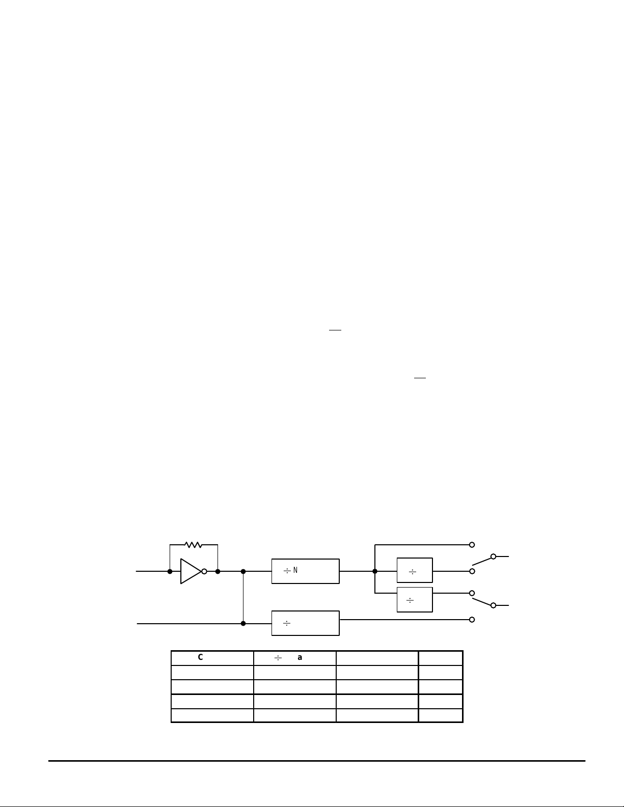
OSC
/OSC
in
Reference Oscillator Input/Output (Pins 7, 8)
These pins form a reference oscillator when connected to
an external parallel–resonant crystal. Figure 6 shows the
relationship of different crystal frequencies and reference
frequencies for cordless phone applications in various countries. OSCin may also serve as input for an externally generated reference signal which is typically ac coupled.
MCUCLK
System Clock (Pin 5)
This output pin provides a signal of the crystal frequency
(OSC
control register.
This signal can be a clock source for the MCU or other system clocks.
ADin, Din, CLK, ENB
Auxiliary Data In, Data In, Clock, Enable (Pins 2, 3, 1, 4)
These four pins provide an MCU serial interface for programming the reference counter, the transmit–channel counter, and the receive–channel counter. They also provide
various controls of the PLL including the power saving mode
and the programming format.
TxPS/fTx, RxPS/f
Transmit Power Save, Receive Power Save (Pins 13, 11)
For a normal application, these output pins provide the
status of the internal power saving mode operation. If the
transmit–channels counter circuitry is in power down mode,
TxPS/fTx outputs a high state. If the receive–channels
counter circuitry is in power down mode, RxPS/fRx is set high.
These outputs can be applied for controlling the external power switch for the transmitter and the receiver to save MCU
control pins.
In the Tx/Rx channel counter test mode, the TxPS/fTx and
RxPS/fRx pins output the divided value of the transmit
channel counter (fTx) and the receive channel counter (fRx),
respectively. This test mode operation is controlled by the
out
) divided by 3 or 4 that is controlled by a bit in the
out
Rx
control register. Details of the counter test mode are in the Tx/
Rx Channel Counter Test section of this data sheet.
fin–T/fin–R
Transmit/Receive Counter Inputs (Pins 14, 9)
fin–T and fin–R are inputs to the transmit and the receive
counters, respectively. These signals are typically driven from
the loop VCO and ac coupled. The minimum input signal level
is 200 mV p–p @ 60.0 MHz.
OUTPUT PINS
TxPD
out
/RxPD
out
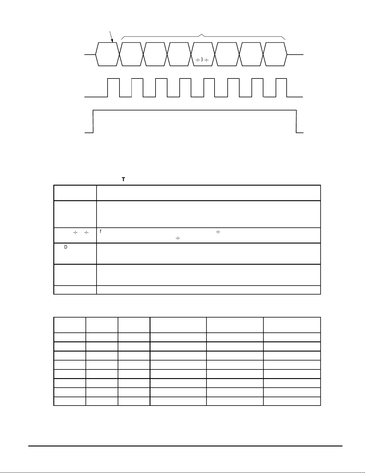
Transmit/Receive Phase Detector Outputs (Pins 15, 10)
These are three–state outputs of the transmit and receive
phase detectors for use as loop error signals (see Figure 7 for
phase detector output waveforms). Phase detector gain is
VDD/4 π volts per radian.
Frequency fV > fR or fV leading: output = negative pulse.
Frequency fV < fR or fV lagging: output = positive pulse.
Frequency fV = fR and phase coincidence: output = high–
impedance state.
NOTE: fR is the divided–down reference frequency at the
phase detector input and fV is the divided–down VCO
frequency at the phase detector input.
LD
Lock Detect (Pin 16)
The lock detect signal is associated with the transmit loop.
The output at a high level indicates an out–of–lock condition
(see Figure 7 for the LD output waveform).
POWER SUPPLY
V
DD
Positive Power Supply (Pin 12)
VDD is the most positive power supply potential ranging
from 2.5 to 5.5 V with respect to VSS.
V
SS
Negative Power Supply (Pin 6)
VSS is the most negative supply potential and is usually
connected to ground.
A
f
f
R1
R2
OSC
OSC
out
in
Crystal
11.150 MHz 446 6.25 kHz 1.0 kHz
11.150 MHz 223 12.5 kHz
10.240 MHz 512 5.0 kHz
12.000 MHz 600 5.0 kHz
N (12 BITS)
M (14 BITS)
N Value
f
R1→B
4
25
f
R2→C
B
C
D
Figure 6. Reference Frequencies for Cordless Phone Applications of Various Countries
MC145162•MC145162–1 MOTOROLA
6

fR, REFERENCE
(OSCin
REFERENCE COUNTER)
fV, FEEDBACK
(fin–T Tx COUNTER OR
fin–R
Rx COUNTER)
TxPD
out
OR
RxPD
out
LD
VH= High voltage level.
VL= Low voltage level.
*At this point, when both fR and fV are in phase, the output is forced to near mid supply.
NOTE: The TxPD
quency, the output is high impedance and the voltage at that pin is determined by the low–pass filter capacitor.
and RxPD
out
generate error pulses during out–of–lock conditions. When locked in phase and fre-
out
Figure 7. Phase Detector/Lock Detector Output Waveforms
V
H
V
L
V
H
V
L
*
V
H
HIGH IMPEDANCE
MCU PROGRAMMING SCHEME
The MCU programming scheme is defined in two formats
controlled by the ENB input. If the enable signal is high during
the serial data transfer, control register/reference frequency
programming is selected. If the ENB is low, programming of
the transmit and receive counters is selected. During programming of the transmit and receive counters, both AD
and Din pins can input the data to the transmit and receive
counters. Both counters’ data is clocked into the PLL internal
shift register at the leading edge of the CLK signal. It is not
necessary to reprogram the reference frequency counter/
control register when using the enable signal to program the
transmit/receive channels.
In programming the control register/reference frequency
scheme, the most significant bit (MSB) of the programming
word identifies whether the input data is the control word or
the reference frequency data word. If the MSB is 1, the input
data is the control word (Figure 8). Also see Figure 8 and
T able 1 for control register and bit function. If the MSB is 0, the
input data is the reference frequency (Figure 9).
The reference frequency data word is a 32–bit word containing the 12–bit reference frequency data, the 14–bit auxiliary reference frequency counter information, the reference
frequency selection plus, the auxiliary reference frequency
counter enable bit (Figure 9).
If the AUX REF ENB bit is high, the 14–bit auxiliary reference frequency counter provides an additional phase reference frequency output for the loops. If AUX REF ENB bit is
low, the auxiliary reference frequency counter is forced into
power–down mode for current saving. (Other power down
modes are also provided through the control register per
Table 2 and Figure 8.) At the falling edge of the ENB signal,
the data is stored in the registers.
There are two interfacing schemes for the universal channel mode: the three–pin and the four–pin interfacing
schemes. The three–pin interfacing scheme is suited for use
with the MCU SPI (serial peripheral interface) (Figure 10),
in
while the four–pin interfacing scheme is commonly used for
general I/O port connection (Figure 11).
For the three–pin interfacing scheme, the auxiliary data
select bit is set to 0. All 32 bits of data, which define both the
16–bit transmit counter and the 16–bit receive counter, latch
into the PLL internal register through the data in pins at the
leading edge of CLK. See Figures 12 and 13.
For the four–pin interfacing scheme, the auxiliary data
select bit is set to 1. In this scheme, the 16–bit transmit counter’s data enters into the ADin pin at the same time as the
16–bit receive counter’s data enters into the Din pin. This simultaneous entry of the transmit and receive counters
causes the programming period of the four–pin scheme to be
half that of the three–pin scheme (see Figures 14 and 15).
While programming Tx/Rx Channel Counter, the ENB pin
must be pulsed to provide falling edge to latch the shifted data
after the rising edge of the last clock. Maximum data transfer
rate is 500 kbps.
NOTE
10 ms should be allowed for initial start–up time
for the oscillator to allow all registers to clear and
enable programming of new register values.
MC145162•MC145162–1MOTOROLA
7
CONTROL REGISTER IDENTIFIER = 1
CONTROL REGISTER DATA
D
in
CLK
ENB
NOTE: ENB must be high during the serial transfer.
10
MSB LSB
TEST
BIT
SELECT
AUX
DATA
REF
OUT
3/
4
TxPD
ENABLE
RxPD
ENABLE
REF PD
ENABLE
Figure 8. Programming Format of the Control Register
Table 1. Control Register Function Bits Description
Test Bit Set to 1 for Tx/Rx channel counter test mode
Aux Data Select Set to 1 for both ADin and Din pins inputting the transmit 16–bits data and receive 16–bits data
REF
3/ 4
out
TxPD Enable If set to 1, the transmit counter, transmit phase detector, and the associated circuitry is in power–
RxPD Enable If set to 1, the receive counter, receive phase detector, and the associated circuitry is in power–
Ref PD Enable If set to 1, both 12–bit and 14–bit reference frequency counters are in power–down mode.
Set to 0 for normal application
respectively.
Set to 0 for normal application interfacing with MCU serial peripheral interface. Does not use ADin pin;
tie ADin to VSS.
If set to 1, REF
If set to 0, REF
down mode.
Tx PS/fTx is set “High”.
down mode.
Rx PS/fRx is set “High”.
output frequency is equal to OSC
out
output is OSC
out
out
4.
out
3.
Table 2. Control Register Power Down Bits Function
TxPD
Enable
0 0 0 — — —
0 0 1 — — Power Down
0 1 0 — Power Down —
0 1 1 — Power Down Power Down
1 0 0 Power Down — —
1 0 1 Power Down — Power Down
1 1 0 Power Down Power Down —
1 1 1 Power Down Power Down Power Down
RxPD
Enable
REF PD
Enable
Tx–Channel Counter Rx–Channel Counter
Reference
Frequency Counter
MC145162•MC145162–1 MOTOROLA
8
 Loading...