

MOTOROLA MC14515BDWR2, MC14515BCP, MC14514BCP, MC14514BDW, MC14514BDWR2 Datasheet
...
MC14514B, MC14515B
4-Bit Transparent
Latch/4-to-16 Line Decoder
The MC14514B and MC14515B are two output options of a 4 to 16
line decoder with latched inputs. The MC14514B (output active high
option) presents a logical “1” at the selected output, whereas the
MC14515B (output active low option) presents a logical “0” at the
selected output. The latches are R–S type flip–flops which hold the
last input data presented prior to the strobe transition from “1” to “0”.
These high and low options of a 4–bit latch/4 to 16 line decoder are
constructed with N–channel and P–channel enhancement mode
devices in a single monolithic structure. The latches are R–S type
flip–flops and data is admitted upon a signal incident at the strobe
input, decoded, and presented at the output.
These complementary circuits find primary use in decoding
applications where low power dissipation and/or high noise immunity
is desired.
• Supply Voltage Range = 3.0 Vdc to 18 Vdc
• Capable of Driving T wo Low–power TTL Loads or One Low–power
Schottky TTL Load Over the Rated T emperature Range
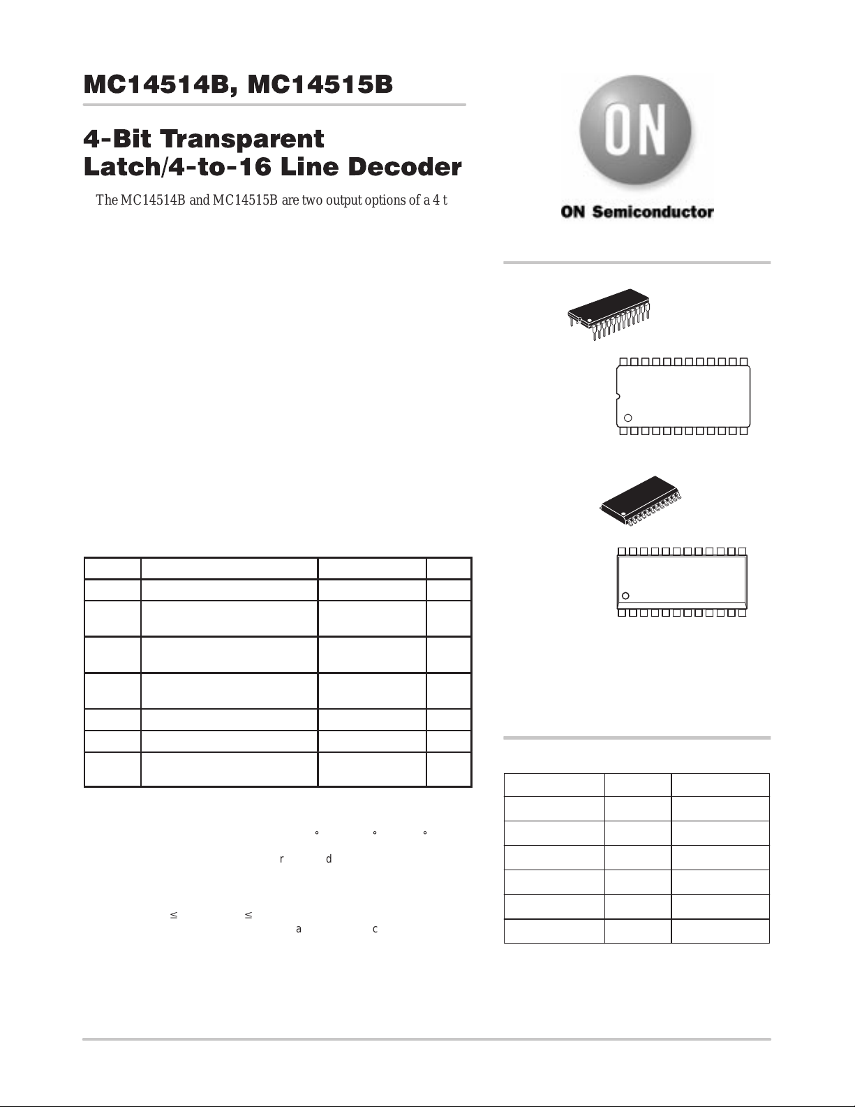
http://onsemi.com
PDIP–24
P SUFFIX
CASE 709
24
MC145XXBCP
1
MARKING
DIAGRAMS
AWLYYWW
MAXIMUM RATINGS (Voltages Referenced to V
Symbol Parameter Value Unit
V
DD
Vin, V
Iin, I
P
T
T
stg
T
1. Maximum Ratings are those values beyond which damage to the device
may occur.
2. Temperature Derating:
Plastic “P and D/DW” Packages: – 7.0 mW/_C From 65_C To 125_C
This device contains protection circuitry to guard against damage due to high
static voltages or electric fields. However, precautions must be taken to avoid
applications of any voltage higher than maximum rated voltages to this
high–impedance circuit. For proper operation, V
to the range V
Unused inputs must always be tied to an appropriate logic voltage level (e.g.,
either V
DC Supply Voltage Range –0.5 to +18.0 V
Input or Output Voltage Range
out
out
D
A
L
(DC or Transient)
Input or Output Current
(DC or Transient) per Pin
Power Dissipation,
per Package (Note 2.)
Ambient Temperature Range –55 to +125 °C
Storage Temperature Range –65 to +150 °C
Lead Temperature
(8–Second Soldering)
v (Vin or V
SS
or VDD). Unused outputs must be left open.
SS
) v VDD.
out
) (Note 1.)
SS
–0.5 to VDD + 0.5 V
±10 mA
500 mW
260 °C
and V
in
should be constrained
out
24
SOIC–24
DW SUFFIX
CASE 751E
XX = Specific Device Code
A = Assembly Location
WL or L = Wafer Lot
YY or Y = Year
WW or W = Work Week
145XXB
AWLYYWW
1
ORDERING INFORMATION
Device Package Shipping
MC14514BCP PDIP–24 15/Rail
MC14514BDW SOIC–24 30/Rail
MC14514BDWR2 SOIC–24 1000/Tape & Reel
MC14515BCP PDIP–24 15/Rail
MC14515BDW SOIC–24 30/Rail
MC14515BDWR2 SOIC–24 1000/Tape & Reel
Semiconductor Components Industries, LLC, 2000
March, 2000 – Rev . 3
1 Publication Order Number:
MC14514B/D
MC14514B, MC14515B
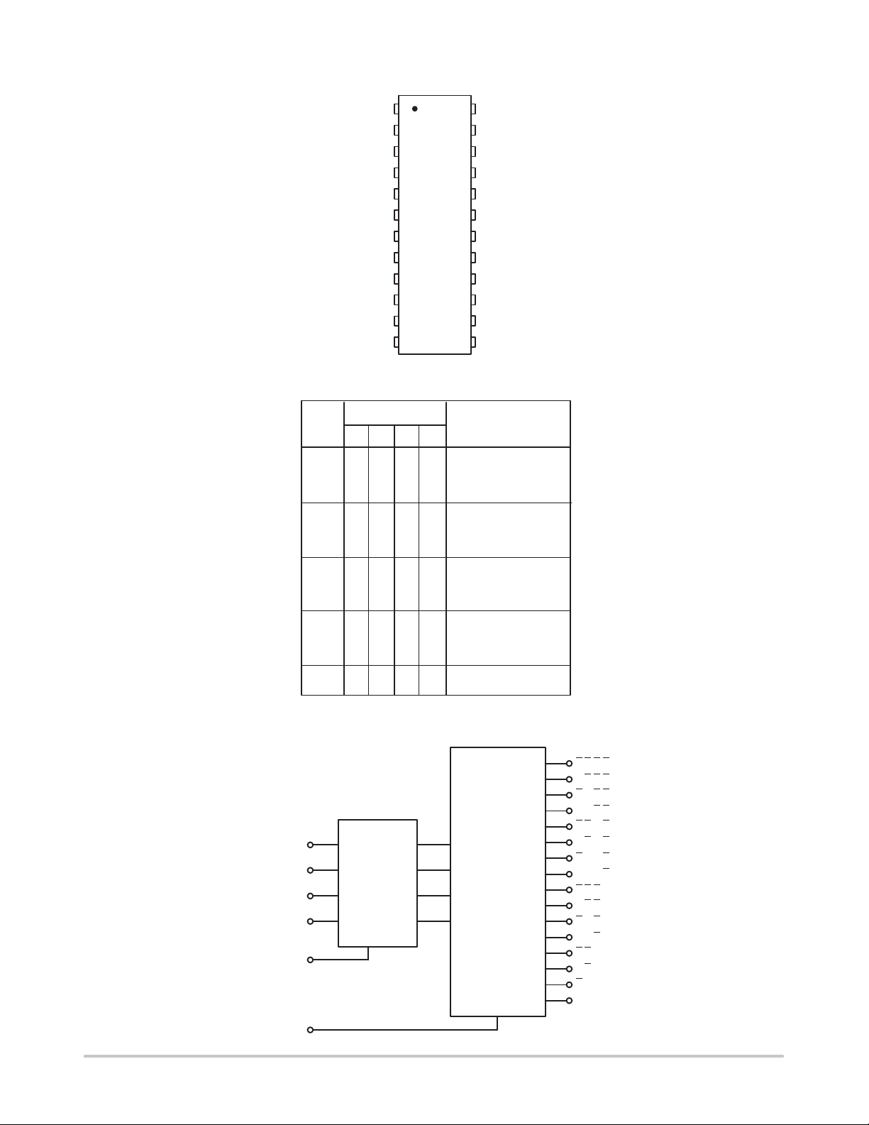
PIN ASSIGNMENT
1
ST
2
D1
3
D2
4
S7
5
S6 S10
S5
6
7
S4
8
S3
9
S1
10
S2
S0
11
V
12
SS
24
V
DD
23
INH
22
D4
21
D3
20
S11
19
S8
18
17
S9
16
S14
15
S15
S12
14
S13
13
DECODE TRUTH TABLE (Strobe = 1)*
Data Inputs
Inhibit D C B A MC14515 = Logic “0”
00000 S0
00001 S1
00010 S2
00011 S3
00100 S4
00101 S5
00110 S6
00111 S7
01000 S8
01001 S9
0 1 0 1 0 S10
01011 S11
0 1 1 0 0 S12
0 1 1 0 1 S13
0 1 1 1 0 S14
0 1 1 1 1 S15
1 X X X X All Outputs = 0, MC14514
X = Don’t Care
*Strobe = 0, Data is latched
Selected Output
MC14514 = Logic “1”
All Outputs = 1, MC14515
BLOCK DIAGRAM
DATA 1
DATA 2
DATA 3
DATA 4
STROBE
INHIBIT
V
DD
V
SS
2
3
TRANSPARENT
21
22
1
23
= PIN 24
= PIN 12
A
B
LATCH
C
D20
http://onsemi.com
2
4 TO 16
DECODER
S0
S1
S2
S3
S4
S5
S6
S7
S8
S9
S10
S11
S12
S13
S14
11
B C D
A
9
A B C D
10
A B C D
8
A B C D
7
A B C D
6
A B C D
5
A B C D
4
A B C D
18
A B C D
17
C D
A B
A
B C D
19
A B C
B C D
A
A B
A
B C D
A B C DS15
D
C D
14
13
16
15
MC14514B, MC14515B
V
DD
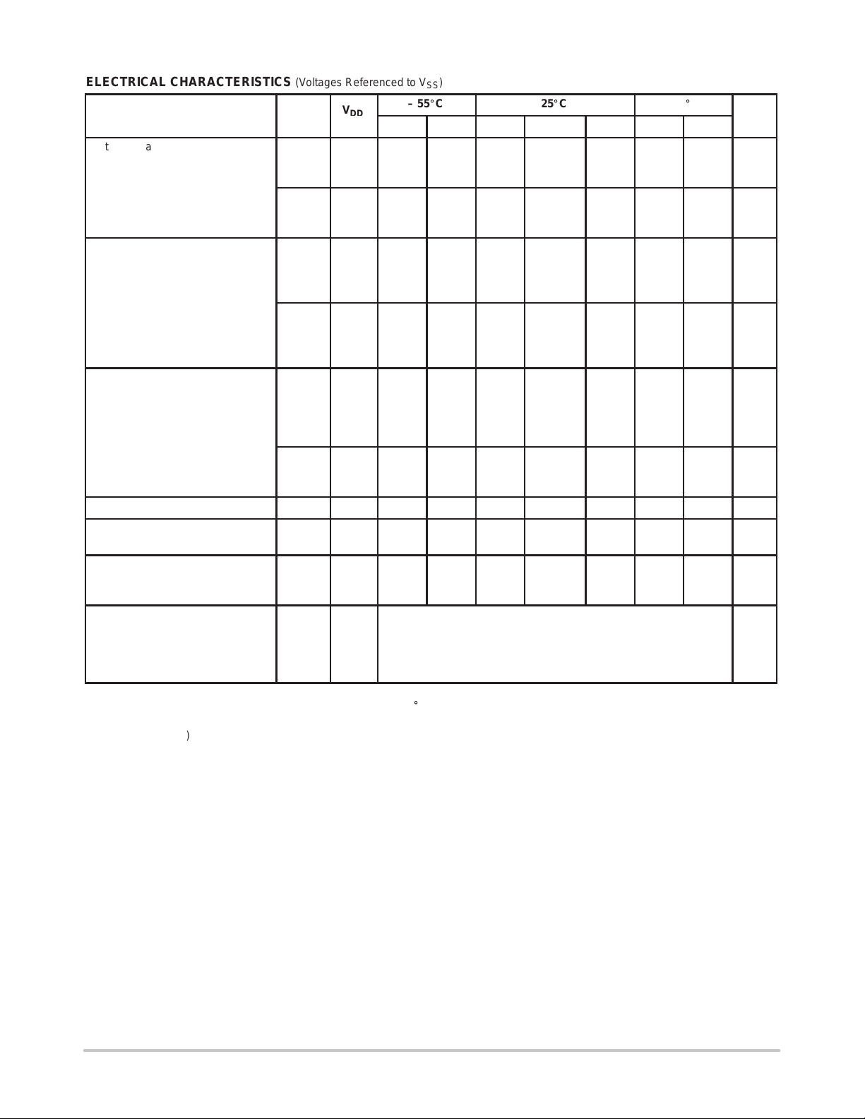
ELECTRICAL CHARACTERISTICS (Voltages Referenced to V
V
Characteristic Symbol
Output Voltage “0” Level
= VDD or 0
V
in
“1” Level
V
= 0 or V
in
DD
Input Voltage “0” Level
(V
= 4.5 or 0.5 Vdc)
O
= 9.0 or 1.0 Vdc)
(V
O
(V
= 13.5 or 1.5 Vdc)
O
“1” Level
= 0.5 or 4.5 Vdc)
(V
O
(V
= 1.0 or 9.0 Vdc)
O
= 1.5 or 13.5 Vdc)
(V
O
Output Drive Current
(V
= 2.5 Vdc) Source
OH
= 4.6 Vdc)
(V
OH
(V
= 9.5 Vdc)
OH
(V
= 13.5 Vdc)
OH
(VOL = 0.4 Vdc) Sink
(V
= 0.5 Vdc)
OL
(V
= 1.5 Vdc)
OL
Input Current I
Input Capacitance
(V
= 0)
in
Quiescent Current
(Per Package)
Total Supply Current
(4.) (5.)
(Dynamic plus Quiescent,
Per Package)
= 50 pF on all outputs, all
(C
L
V
OL
V
OH
V
V
I
OH
I
OL
in
C
I
DD
I
TL
Vdc
5.0
10
15
5.0
10
15
IL
5.0
10
15
IH
5.0
10
15
5.0
5.0
10
15
5.0
10
15
Min Max Min Typ
—
—
—
4.95
9.95
14.95
—
—
—
3.5
7.0
11
– 1.2
– 0.25
– 0.62
– 1.8
0.64
1.6
4.2
15 — ± 0.1 — ±0.00001 ± 0.1 — ± 1.0 µAdc
in
— — — — 5.0 7.5 — — pF
5.0
10
15
—
—
—
5.0
10
15
)
SS
– 55_C 25_C 125_C
(3.)
Max Min Max
0.05
0.05
0.05
—
—
—
1.5
3.0
4.0
—
—
—
—
—
—
—
—
—
—
5.0
10
20
—
—
—
4.95
9.95
14.95
—
—
—
3.5
7.0
11
– 1.0
– 0.2
– 0.5
– 1.5
0.51
1.3
3.4
—
—
—
0
0
0
5.0
10
15
2.25
4.50
6.75
2.75
5.50
8.25
– 1.7
– 0.36
– 0.9
– 3.5
0.88
2.25
8.8
0.005
0.010
0.015
IT = (1.35 µA/kHz) f + I
IT = (2.70 µA/kHz) f + I
IT = (4.05 µA/kHz) f + I
0.05
0.05
0.05
—
—
—
1.5
3.0
4.0
—
—
—
—
—
—
—
—
—
—
5.0
10
20
DD
DD
DD
—
—
—
4.95
9.95
14.95
—
—
—
3.5
7.0
11
– 0.7
– 0.14
– 0.35
– 1.1
0.36
0.9
2.4
—
—
—
0.05
0.05
0.05
150
300
600
buffers switching)
3. Data labelled “Typ” is not to be used for design purposes but is intended as an indication of the IC’s potential performance.
4. The formulas given are for the typical characteristics only at 25_C.
5. To calculate total supply current at loads other than 50 pF:
I
) = IT(50 pF) + (CL – 50) Vfk
T(CL
where: I
is in µA (per package), CL in pF, V = (VDD – VSS) in volts, f in kHz is input frequency, and k = 0.002.
T
—
—
—
1.5
3.0
4.0
—
—
—
—
—
—
—
—
—
—
Unit
Vdc
Vdc
Vdc
Vdc
mAdc
mAdc
µAdc
µAdc
http://onsemi.com
3
MC14514B, MC14515B
SWITCHING CHARACTERISTICS
(6.)
(C
= 50 pF, T
L
= 25_C)
A
All Types
Characteristic Symbol V
Output Rise Time
t
= (3.0 ns/pF) CL + 30 ns
TLH
= (1.5 ns/pF) CL + 15 ns
t
TLH
t
= (1.1 ns/pF) CL + 10 ns
TLH
Output Fall Time
t
= (1.5 ns/pF) CL + 25 ns
THL
= (0.75 ns/pF) CL + 12.5 ns
t
THL
t
= (0.55 ns/pF) CL + 9.5 ns
THL
Propagation Delay Time; Data, Strobe to S
t
, t
PLH
t
PLH
t
PLH
= (1.7 ns/pF) CL + 465 ns
PHL
, t
= (0.86 ns/pF) CL + 192 ns
PHL
, t
= (0.5 ns/pF) CL + 125 ns
PHL
Inhibit Propagation Delay Times
t
, t
PLH
t
PLH
t
PLH
= (1.7 ns/pF) CL + 315 ns
PHL
, t
= (0.66 ns/pF) CL + 117 ns
PHL
, t
= (0.5 ns/pF) CL + 75 ns
PHL
Setup Time
Data to Strobe
Hold Time
Strobe to Data
Strobe Pulse Width t
t
t
t
TLH
t
THL
PLH
t
PHL
PLH
t
PHL
t
WH
DD
5.0
10
15
5.0
10
15
Min Typ
—
—
—
—
—
—
,
5.0
10
15
—
—
—
,
5.0
10
15
su
5.0
10
15
t
h
5.0
10
15
5.0
10
15
—
—
—
250
100
75
– 20
0
10
350
100
75
(7.)
180
90
65
100
50
40
550
225
150
400
150
100
125
50
38
– 100
– 40
– 30
175
50
38
6. The formulas given are for the typical characteristics only at 25_C.
7. Data labelled “Typ” is not to be used for design purposes but is intended as an indication of the IC’s potential performance.
Max
360
180
130
200
100
80
1100
450
300
800
300
200
—
—
—
—
—
—
—
—
—
Unit
ns
ns
ns
ns
ns
ns
ns
For MC14514B
1. For P–channel: Inhibit = V
1. and D1–D4 constitute
1. binary code for “output
1. under test.”
2. For N–channel: Inhibit = V
SS
DD
V
DD
S0
STROBE
INHIBIT
S1
S2
S3
S4
S5
S10
S11
S12
S13
S14
S6
S7
S8
S9
I
D
EXTERNAL
POWER SUPPLY
D1
D2
D3
D4
S15
V
SS
Figure 1. Drain Characteristics T est Circuit
V
DS
For MC14515B
1. For P–channel: Inhibit = V
2. For N–channel: Inhibit = V
2. and D1–D4 constitute binary
2. code for “output
DD
SS
under test.”
http://onsemi.com
4
 Loading...