Motorola MC145149P, MC145149DW Datasheet

MC145149MOTOROLA
1
Interfaces with Dual–Modulus Prescalers
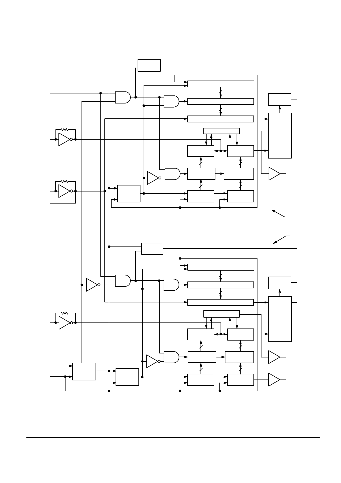
The MC145149 contains two PLL Frequency Synthesizers which share a
common serial data port and common reference oscillator. The device
contains two 14–stage R counters, two 10–stage N counters, and two
7–stage A counters. All six counters are fully programmable through a serial
port. The divide ratios are latched into the appropriate counter latch
according to the last data bits (control bits) entered.
When combined with external low–pass filters and voltage controlled
oscillators (VCOs), the MC145149 can provide all the remaining functions
for two PLL frequency synthesizers operating up to the device’s frequency
limit. For higher VCO frequency operation, a down mixer or dual–modulus
prescaler can be used between the VCO and the synthesizer IC.
• Low Power Consumption Through Use of CMOS Technology
• Wide Operating Voltage Range: 3 to 9 V
• Operating Temperature Range: – 40 to + 85°C
•÷ R Range = 3 to 16,383
•÷ N Range = 3 to 1023
•÷ A Range = 0 to 127
• Two “Linearized” Three–State Digital Phase Detectors with No Dead Zone
• Two Lock Detect Signals (LD1 and LD2)
• Two Open–Drain Port Expander Outputs (SW1 and SW2)
• Compatible with the Serial Peripheral Interface (SPI) on CMOS MCUs
Order this document
by MC145149/D
SEMICONDUCTOR TECHNICAL DATA
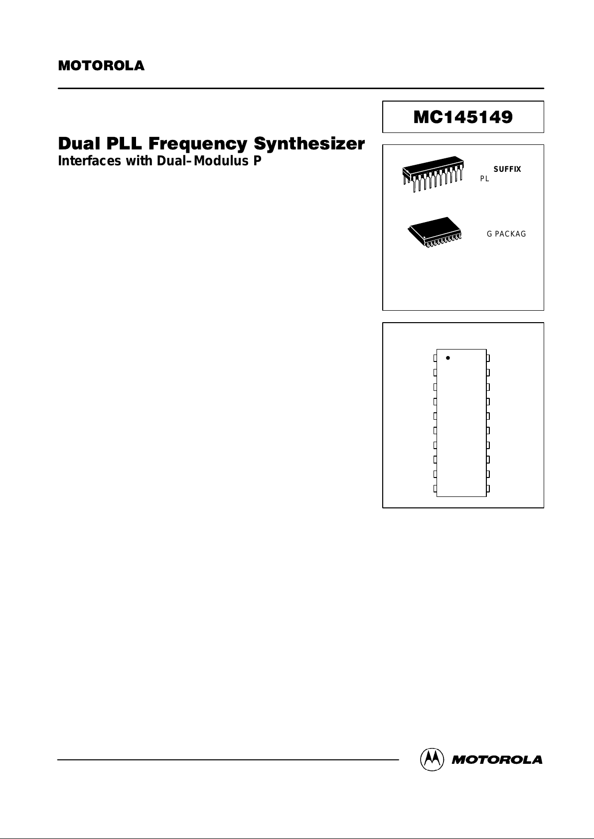
P SUFFIX
PLASTIC DIP
CASE 738
DW SUFFIX
SOG PACKAGE
CASE 751D
ORDERING INFORMATION
MC145149P Plastic DIP
MC145149DW SOG Package
20
1
20
1
CLK
f
in1
ENB
MC1
LD1
LD2
MC2
S/R
out
f
in2
DATA 5
4
3
2
1
10
9
8
7
6
14
15
16
17
18
19
20
11
12
13
OSC
out
SW1
V
DD1
PD
out1
V
SS1
V
SS2
PD
out2
V
DD2
SW2
OSC
in
PIN ASSIGNMENT
Motorola, Inc. 1995

MC145149 MOTOROLA
2
CLK
DATA
6
5
PLL2
PLL1
SW1
17
SW2
14
10
10
7
7
14
14
10
10
7
7
14
14
8
2–BIT
CONTROL
S/R
7
10–BIT S/R7–BIT S/R
÷
A COUNTER
LATCH
10–BIT ÷ N
COUNTER
7–BIT ÷ A
COUNTER
MODULUS
CONTROL 2
(MC2)
9
12
10
LOCK
DETECT
14–BIT
÷
R COUNTER
1–BIT
LATCH
1–BIT
CONTROL
S/R
REFERENCE COUNTER LATCH
CONTROL LOGIC
PHASE
DETECTOR
÷
N COUNTER
LATCH
14–BIT SHIFT REGISTER
16
15
4
ENB
3
10–BIT S/R7–BIT S/R
÷
A COUNTER
LATCH
10–BIT
÷
N
COUNTER
7–BIT ÷ A
COUNTER
MODULUS
CONTROL 1
(MC1)
2
19
1
LOCK
DETECT
14–BIT
÷
R COUNTER
1–BIT
LATCH
1–BIT
CONTROL
S/R
REFERENCE COUNTER LATCH
CONTROL LOGIC
PHASE
DETECTOR
÷
N COUNTER
LATCH
14–BIT SHIFT REGISTER
OSC
in
OSC
out
f
in1
f
in2
S/R
out
PD
out2
f
R
PIN 13
=
V
DD2
PIN 11
=
V
SS2
PD
out1
f
R
PIN 18
=
V
DD1
PIN 20
=
V
SS1
BLOCK DIAGRAM
f
V
f
V
LD2
LD1

MC145149MOTOROLA
3
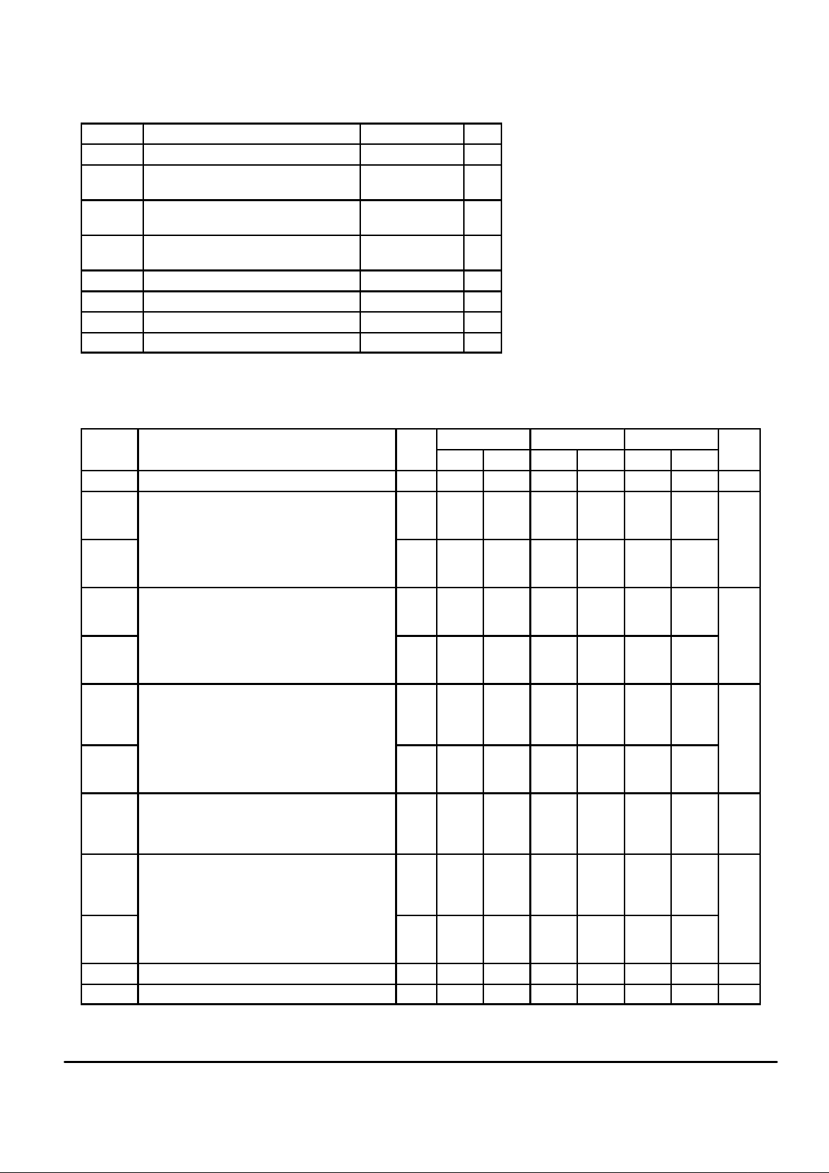
MAXIMUM RATINGS* (Voltages Referenced to V
SS
)
Symbol Rating Value Unit
V
DD
DC Supply Voltage – 0.5 to + 10 V
Vin, V
out
Input or Output Voltage (DC or T ransient)
except SW1, SW2
– 0.5 to VDD + 0.5 V
V
out
Output Voltage (DC or Transient) — SW1,
SW2
– 0.5 to 15 V
Iin, I
out
Input or Output Current (DC or Transient),
per Pin
± 10 mA
IDD, I
SS
Supply Current, VDD or VSS Pins ± 30 mA
P
D
Power Dissipation, per Package† 500 mW
T
stg
Storage Temperature – 65 to + 150 °C
T
L
Lead T emperature (8–Second Soldering) 260 °C
*Maximum Ratings are those values beyond which damage to the device may occur.
†Power Dissipation Temperature Derating:
Plastic DIP: – 12 mW/°C from 65 to 85°C
SOG Package: – 7 mW/°C from 65 to 85°C
ELECTRICAL CHARACTERISTICS (Voltages Referenced to V
SS
)
V
– 40°C 25°C 85°C
Symbol Characteristic
V
DD
V
Min Max Min Max Min Max
Unit
V
DD
Power Supply Voltage Range — 3 9 3 9 3 9 V
V
OL
Output Voltage 0 Level
Vin = 0 V or V
DD
I
out
= 0 µA
3
5
9
—
—
—
0.05
0.05
0.05
—
—
—
0.05
0.05
0.05
—
—
—
0.05
0.05
0.05
V
V
OH
1 Level 3
5
9
2.95
4.95
8.95
—
—
—
2.95
4.95
8.95
—
—
—
2.95
4.95
8.95
—
—
—
V
IL
Input Voltage 0 Level
V
out
= 0.5 V or VDD – 0.5 V
(All Outputs Except OSC
out
)
3
5
9
—
—
—
0.9
1.5
2.7
—
—
—
0.9
1.5
2.7
—
—
—
0.9
1.5
2.7
V
V
IH
1 Level 3
5
9
2.1
3.5
6.3
—
—
—
2.1
3.5
6.3
—
—
—
2.1
3.5
6.3
—
—
—
I
OH
Output Current — MC1, MC2
V
out
= 2.7 V Source
V
out
= 4.6 V
V
out
= 8.5 V
3
5
9
– 0.60
– 0.90
– 1.50
—
—
—
– 0.50
– 0.75
– 1.25
—
—
—
– 0.30
– 0.50
– 0.80
—
—
—
mA
I
OL
V
out
= 0.3 V Sink
V
out
= 0.4 V
V
out
= 0.5 V
3
5
9
1.30
1.90
3.80
—
—
—
1.10
1.70
3.30
—
—
—
0.66
1.08
2.10
—
—
—
I
OL
Output Current — SW1, SW2
V
out
= 0.3 V Sink
V
out
= 0.4 V
V
out
= 0.5 V
3
5
9
0.80
1.50
3.50
—
—
—
0.48
0.90
2.10
—
—
—
0.24
0.45
1.50
—
—
—
mA
I
OH
Output Current — Other Outputs
V
out
= 2.7 V Source
V
out
= 4.6 V
V
out
= 8.5 V
3
5
9
– 0.44
– 0.64
– 1.30
—
—
—
– 0.35
– 0.51
– 1.00
—
—
—
– 0.22
– 0.36
– 0.70
—
—
—
mA
I
OL
V
out
= 0.3 V Sink
V
out
= 0.4 V
V
out
= 0.5 V
3
5
9
0.44
0.64
1.30
—
—
—
0.35
0.51
1.00
—
—
—
0.22
0.36
0.70
—
—
—
I
in
Input Current — DATA, CLK, ENB 9 — ± 0.3 — ± 0.1 — ± 1.0 µA
I
in
Input Current — fin, OSC
in
9 — ± 50 — ± 25 — ± 22 µA
(continued)
This device contains circuitry to protect
against damage due to high static voltages or
electric fields, however, it is advised that normal
precautions be taken to avoid applications of any
voltage higher than maximum rated voltages to
this high–impedance circuit. For proper operation, it is recommended that Vin and V
out
be
constrained to the range VSS≤ (Vin or
V
out
) ≤ VDD except SW1 and SW2 which may
range up to 15 V.
Unused inputs must always be tied to an
appropriate logic voltage level (e.g., either V
SS
or VDD). Unused outputs should be left floating.

MC145149 MOTOROLA
4
ELECTRICAL CHARACTERISTICS (continued)
V
– 40°C 25°C 85°C
Symbol Characteristic
V
DD
V
Min Max Min Max Min Max
Unit
C
in
Input Capacitance — — 10 — 10 — 10 pF
C
out
Three–State Output Capacitance — PD
out
— — 10 — 10 — 10 pF
I
DD
Quiescent Current
Vin = 0 V or V
DD
I
out
= 0 µA
3
5
9
—
—
—
800
1200
1600
—
—
—
800
1200
1600
— 1600
2400
3200
µA
I
OZ
Three–State Leakage Current — PD
out
V
out
= 0 V or 9 V
9 — ± 0.3 — ± 0.1 — ± 3.0 µA
I
OZ
Off–State Leakage Current — SW1, SW2
V
out
= 9 V
9 — 0.3 — 0.1 — 3.0 µA
SWITCHING CHARACTERISTICS (T
A
= 25°C, CL = 50 pF)
Symbol
Characteristic
Figure
No.
V
DD
V
Min Max Unit
t
TLH
Output Rise Time, MC1 and MC2 1, 6 3
5
9
—
—
—
115
60
40
ns
t
THL
Output Fall Time, MC1 and MC2 1, 6 3
5
9
—
—
—
60
34
30
ns
t
TLH
,
t
THL
Output Rise and Fall Time, LD and S/R
out
1, 6 3
5
9
—
—
—
140
80
60
ns
t
PLH
,
t
PHL
Propagation Delay Time, fin to MC1 or MC2 2, 6 3
5
9
—
—
—
125
80
50
ns
t
su
Setup Time, DATA to CLK 3 3
5
9
30
20
18
—
—
—
ns
t
su
Setup Time, CLK to ENB 3 3
5
9
70
32
25
—
—
—
ns
t
h
Hold Time, CLK to DATA 3 3
5
9
12
12
15
—
—
—
ns
t
rec
Recovery Time, ENB to CLK 3 3
5
9
5
10
20
—
—
—
ns
tr, t
f
Input Rise and Fall Times, Any Input 4 3
5
9
—
—
—
5
2
0.5
µs
t
w
Input Pulse Width, ENB and CLK 5 3
5
9
40
35
25
—
—
—
ns
 Loading...