

MOTOROLA MC14513BCP Datasheet
MC14513B
BCD-To-Seven Segment
Latch/Decoder/Driver
CMOS MSI
(Low–Power Complementary MOS)
The MC14513B BCD–to–seven segment latch/decoder/driver is
constructed with complementary MOS (CMOS) enhancement mode
devices and NPN bipolar output drivers in a single monolithic structure.
The circuit provides the functions of a 4–bit storage latch, an 8421
BCD–to–seven segment decoder, and has output drive capability. Lamp
test (L T
), blanking (BI), and latch enable (LE) inputs are used to test the
display, to turn–off or pulse modulate the brightness of the display, and
to store a BCD code, respectively. The Ripple Blanking Input (RBI) and
Ripple Blanking Output (RBO) can be used to suppress either leading
or trailing zeroes. It can be used with seven–segment light emitting
diodes (LED), incandescent, fluorescent, gas discharge, or liquid crystal
readouts either directly or indirectly.
Applications include instrument (e.g., counter, DVM, etc.) display
driver, computer/calculator display driver, cockpit display driver, and
various clock, watch, and timer uses.
• Low Logic Circuit Power Dissipation
• High–current Sourcing Outputs (Up to 25 mA)
• Latch Storage of Binary Input
• Blanking Input
• Lamp T est Provision
• Readout Blanking on all Illegal Input Combinations
• Lamp Intensity Modulation Capability
• Time Share (Multiplexing) Capability
• Adds Ripple Blanking In, Ripple Blanking Out to MC14511B
• Supply Voltage Range = 3.0 V to 18 V
• Capable of Driving T wo Low–Power TTL Loads, One Low–power
Schottky TTL Load to T wo HTL Loads Over the Rated Temperature
Range.
MAXIMUM RATINGS (Voltages Referenced to V
Symbol Parameter Value Unit
V
V
P
T
T
I
OHmax
P
OHmax
DD
stg
DC Supply Voltage Range –0.5 to +18.0 V
Input Voltage Range, All Inputs –0.5 to VDD + 0.5 V
in
I DC Current Drain per Input Pin 10 mA
Power Dissipation,
D
A
per Package
Operating Temperature Range –55 to +125 °C
Storage Temperature Range –65 to +150 °C
Maximum Continuous Output
Drive Current (Source) per Output
Maximum Continuous Output
Power (Source) per Output
(2.)
(3.)
(1.)
)
SS
500 mW
25 mA
50 mW
http://onsemi.com
MARKING
DIAGRAMS
18
PDIP–18
P SUFFIX
CASE 707
A = Assembly Location
WL or L = Wafer Lot
YY or Y = Year
WW or W = Work Week
MC14513BCP
AWLYYWW
1
ORDERING INFORMATION
Device Package Shipping
MC14513BCP PDIP–18 20/Rail
This device contains protection circuitry to protect
the inputs against damage due to high static voltages
or electric fields. However, it is advised that normal
precautions be taken to avoid application of any voltage higher than maximum rated voltages to this high–
impedance circuit. A destructive high current mode
may occur if V
range V
Due to the sourcing capability of this circuit, damage can occur to the device if V
outputs are shorted to V
Maximum Ratings).
Unused inputs must always be tied to an appropriate logic voltage level (e.g., either V
1. Maximum Ratings are those values beyond which
damage to the device may occur.
2. Temperature Derating:
Plastic “P and D/DW” Packages: – 7.0 mW/_C
From 65_C To 125_C
3. P
OHmax
and V
in
v (Vin or V
SS
= IOH (VDD – VOH)
are not constrained to the
out
) v VDD.
out
is applied, and the
DD
and are at a logical 1 (See
SS
or VDD).
SS
Semiconductor Components Industries, LLC, 2000
March, 2000 – Rev . 3
1 Publication Order Number:
MC14513B/D
MC14513B
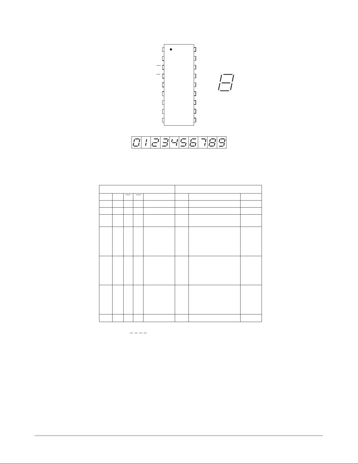
PIN ASSIGNMENT
B
1
C
2
LT
3
BI
4
LE
5
D
6
A
7
8
RBI
V
9
SS
DISPLAY
0123456789
TRUTH TABLE
Inputs Outputs
RBI LE BI LT D C B A RBO a b c d e f g Display
X X X 0 XXXX + 1111111 8
X X 0 1 X X X X + 0 0 0 0 0 0 0 Blank
1 0 1 1 0 0 0 0 1 0 0 0 0 0 0 0 Blank
0 0 1 1 0000 0 1111110 0
X 0 1 1 0 0 01 0 0110000 1
X 0 1 1 0010 0 1101101 2
X 0 1 1 0011 0 1111001 3
X 0 1 1 0100 0 0110011 4
X 0 1 1 0101 0 1011011 5
X 0 1 1 0110 0 1011111 6
X 0 1 1 0111 0 1110000 7
X 0 1 1 1000 0 1111111 8
X 0 1 1 1001 0 1111011 9
X 0 1 1 1 0 1 0 0 0 0 0 0 0 0 0 Blank
X 0 1 1 1 0 1 1 0 0 0 0 0 0 0 0 Blank
X 0 1 1 1 1 0 0 0 0 0 0 0 0 0 0 Blank
X 0 1 1 1 1 0 1 0 0 0 0 0 0 0 0 Blank
X 0 1 1 1 1 1 0 0 0 0 0 0 0 0 0 Blank
X 0 1 1 1 1 1 1 0 0 0 0 0 0 0 0 Blank
X 1 1 1 X X X X † * *
X = Don’t Care
†RBO = RBI (D
*Depends upon the BCD code previously applied when LE = 0
C B A), indicated by other rows of table
V
18
DD
f
17
g
16
a
15
b
14
c
13
d
12
e
11
RBO
10
fg
e
d
a
b
c
http://onsemi.com
2
MC14513B
V
DD
(4.)
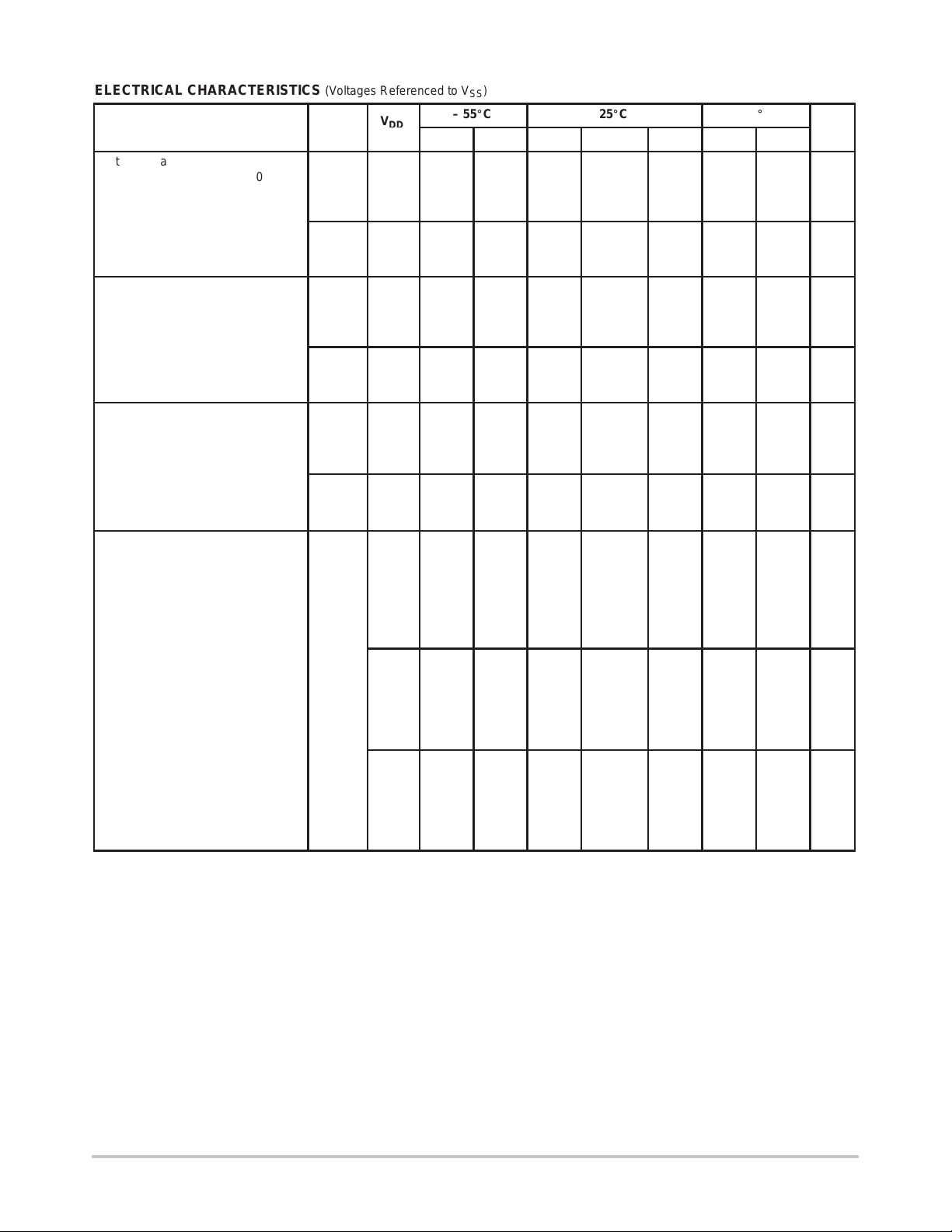
ELECTRICAL CHARACTERISTICS (Voltages Referenced to V
– 55_C 25_C 125_C
Min Max Min Typ
—
—
—
4.1
9.1
14.1
—
—
—
4.95
9.95
14.95
—
—
—
3.5
7.0
11
—
3.9
—
3.4
—
—
9.0
—
8.6
—
—
14
—
13.6
—
Characteristic Symbol
Output Voltage — Segment Outputs
“0” Level
= VDD or 0
V
in
“1” Level
= 0 or V
V
in
DD
Output Voltage — RBO Output
“0” Level
= VDD or 0
V
in
“1” Level
V
= 0 or V
in
Input Voltage
(V
O
(V
O
(V
O
DD
“0” Level
= 3.8 or 0.5 Vdc)
= 8.8 or 1.0 Vdc)
= 13.8 or 1.5 Vdc)
(VO = 0.5 or 3.8 Vdc) “1” Level
(V
= 1.0 or 8.8 Vdc)
O
(V
= 1.5 or 13.8 Vdc)
O
Output Drive Voltage — Segments
(I
= 0 mA) Source
OH
(I
= 5.0 mA)
OH
(I
= 10 mA)
OH
= 15 mA)
(I
OH
(I
= 20 mA)
OH
(I
= 25 mA)
OH
(IOH = 0 mA)
(I
= 5.0 mA)
OH
(I
= 10 mA)
OH
(I
= 15 mA)
OH
= 20 mA)
(I
OH
(I
= 25 mA)
OH
(IOH = 0 mA)
= 5.0 mA)
(I
OH
(I
= 10 mA)
OH
(I
= 15 mA)
OH
(I
= 20 mA)
OH
(I
= 25 mA)
OH
V
Vdc
V
OL
5.0
10
15
V
OH
5.0
10
15
V
OL
5.0
10
15
V
OH
5.0
10
15
V
IL
5.0
10
15
V
IH
5.0
10
15
V
OH
5.0 4.1
10 9.1
15 14.1
SS
)
0.05
0.05
0.05
0.05
0.05
0.05
—
—
—
—
—
—
1.5
3.0
4.0
—
—
—
—
—
—
—
—
—
—
—
—
—
—
—
—
—
—
—
—
—
—
—
—
4.1
9.1
14.1
—
—
—
4.95
9.95
14.95
—
—
—
3.5
7.0
11
4.1
—
3.9
—
3.4
—
9.1
—
9.0
—
8.6
—
14.1
—
14
—
13.6
—
0
0
0
5.0
10
15
0
0
0
5.0
10
15
2.25
4.50
6.75
2.75
5.50
8.25
4.57
4.24
4.12
3.94
3.70
3.54
9.58
9.26
9.17
9.04
8.90
8.75
14.59
14.27
14.18
14.07
13.95
13.80
(4.)
Max Min Max
0.05
0.05
0.05
—
—
—
0.05
0.05
0.05
—
—
—
1.5
3.0
4.0
—
—
—
—
—
—
—
—
—
—
—
—
—
—
—
—
—
—
—
—
—
—
—
—
4.1
9.1
14.1
—
—
—
4.95
9.95
14.95
—
—
—
3.5
7.0
11
4.1
—
3.5
—
3.0
—
9.1
—
8.6
—
8.2
—
14.1
—
13.6
—
13.2
—
0.05
0.05
0.05
—
—
—
0.05
0.05
0.05
—
—
—
1.5
3.0
4.0
—
—
—
—
—
—
—
—
—
—
—
—
—
—
—
—
—
—
—
—
—
Unit
Vdc
Vdc
Vdc
Vdc
Vdc
Vdc
Vdc
Vdc
Vdc
(continued)
http://onsemi.com
3
MC14513B
V
DD
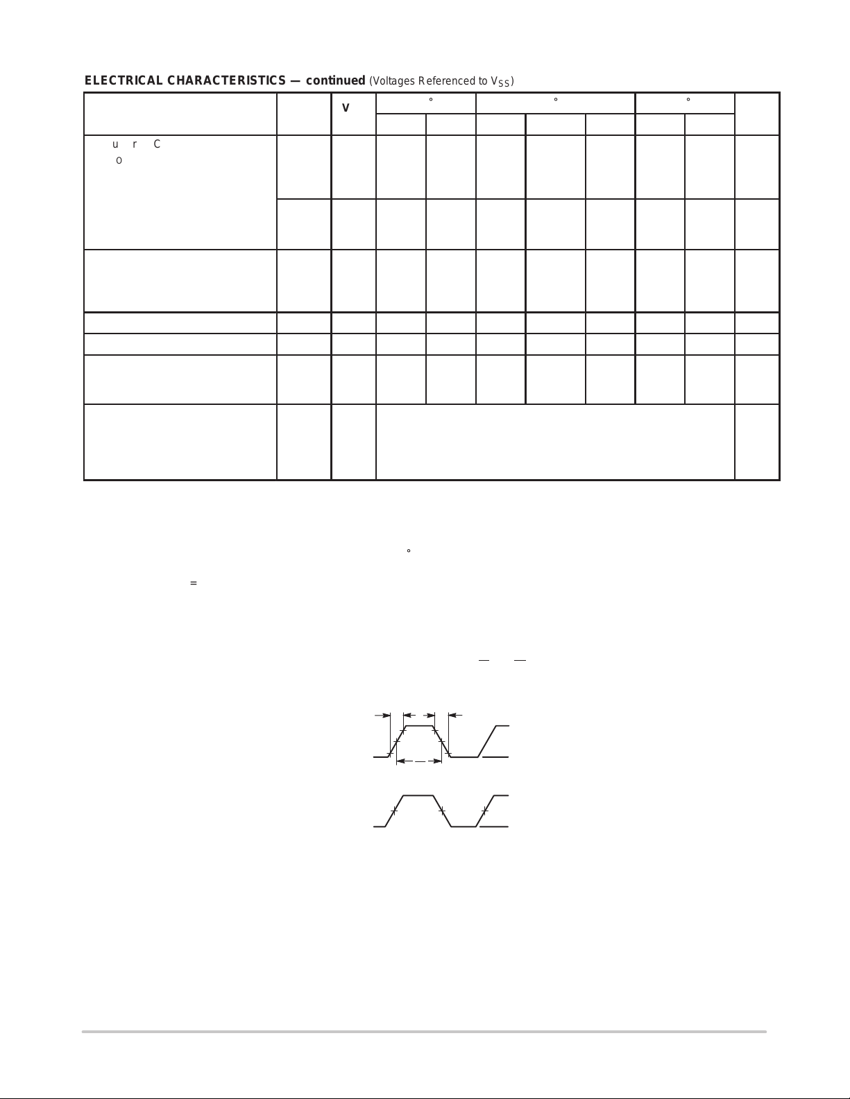
ELECTRICAL CHARACTERISTICS — continued (Voltages Referenced to V
V
Characteristic Symbol
Output Drive Current — RBO Output
= 2.5 V) Source
(V
OH
= 9.5 V)
(V
OH
(V
= 13.5 V)
OH
(VOL = 0.4 V) Sink
= 0.5 V)
(V
OL
(V
= 1.5 V)
OL
Output Drive Current — Segments
(V
= 0.4 V) Sink
OL
= 0.5 V)
(V
OL
(V
= 1.5 V)
OL
Input Current I
Input Capacitance C
Quiescent Current
(Per Package) V
= 0 µA
I
out
Total Supply Current
= 0 or VDD,
in
(5.) (6.)
(Dynamic plus Quiescent,
Per Package)
= 50 pF on all outputs, all
(C
L
I
OH
I
OL
I
OL
in
I
DD
I
Vdc
5.0
10
15
5.0
10
15
5.0
10
15
15 — ± 0.1 — ±0.00001 ± 0.1 — ± 1.0 µAdc
in
— — — — 5.0 7.5 — — pF
5.0
10
15
T
5.0
10
15
buffers switching)
4. Noise immunity specified for worst–case input combination.
Noise Margin for both “1” and “0” level =
1.0 Vdc min @ V
2.0 Vdc min @ V
2.5 Vdc min @ V
5. The formulas given are for the typical characteristics only at 25_C.
= 5.0 Vdc
DD
= 10 Vdc
DD
= 15 Vdc
DD
6. To calculate total supply current at loads other than 50 pF:
I
) = IT(50 pF) + 3.5 x 10⁻³ (CL – 50) VDDf
T(CL
where: I
is in µA (per package), CL in pF, VDD in Vdc, and f in kHz is input frequency.
T
– 55_C 25_C 125_C
Min Max Min Typ
– 0.40
– 0.21
– 0.81
0.18
0.47
1.80
0.64
1.6
4.2
—
—
—
—
—
—
—
—
—
—
—
—
5.0
10
20
– 0.32
– 0.17
– 0.66
)
SS
(4.)
– 0.64
– 0.34
– 1.30
0.15
0.38
1.50
0.51
1.3
3.4
—
—
—
0.29
0.75
2.90
0.88
2.25
8.8
0.005
0.010
0.015
IT = (1.9 µA/kHz) f + I
IT = (3.8 µA/kHz) f + I
IT = (5.7 µA/kHz) f + I
Max Min Max
—
5.0
DD
DD
DD
—
—
—
—
—
—
—
—
10
20
– 0.22
– 0.12
– 0.46
0.10
0.26
1.0
0.36
0.9
2.4
—
—
—
—
—
—
—
—
—
—
—
—
150
300
600
Unit
mAdc
mAdc
mAdc
µAdc
µAdc
Input LE and RBI low, and Inputs D, BI and LT high.
f in respect to a system clock.
10%
20 ns
loads.
L
V
DD
V
SS
All outputs connected to respective C
20 ns
A, B, AND C
90%
50%
1
2f
ANY OUTPUT
50% DUTY CYCLE
50%
V
OH
V
OL
Figure 1. Dynamic Power Dissipation Signal Waveforms
http://onsemi.com
4
 Loading...