

Motorola MC14511BCP, MC14511BD, MC14511BDW, MC14511BCL Datasheet
MOTOROLA CMOS LOGIC DATA
361
MC14511B
The MC14511B BCD–to–seven s egment latch/decoder/driver is
constructed with complementary MOS (CMOS) enhancement mode devices
and NPN bipolar output drivers in a single monolithic structure. The circuit
provides the functions of a 4–bit storage latch, an 8421 BCD–to–seven
segment decoder, and an output drive capability. Lamp test (LT
), blanking
(BI
), and latch enable (LE) inputs are used to test the display, to turn–off or
pulse modulate the brightness of the display, and to store a BCD code,
respectively. It can be used with seven–segment light–emitting diodes
(LED), incandescent, fluorescent, gas discharge, or liquid crystal readouts
either directly or indirectly.
Applications include instrument (e.g., counter, DVM, etc.) display driver,
computer/calculator display driver, cockpit display driver, and various clock,
watch, and timer uses.
• Low Logic Circuit Power Dissipation
• High–Current Sourcing Outputs (Up to 25 mA)
• Latch Storage of Code
• Blanking Input
• Lamp Test Provision
• Readout Blanking on all Illegal Input Combinations
• Lamp Intensity Modulation Capability
• Time Share (Multiplexing) Facility
• Supply Voltage Range = 3.0 V to 18 V
• Capable of Driving Two Low–power TTL Loads, One Low–power
Schottky TTL Load or Two HTL Loads Over the Rated Temperature
Range
• Chip Complexity: 216 FETs or 54 Equivalent Gates
• Triple Diode Protection on all Inputs
MAXIMUM RATINGS* (Voltages Referenced to V
SS
)
Rating
Symbol Value Unit
DC Supply Voltage V
DD
– 0.5 to + 18 V
Input Voltage, All Inputs V
in
– 0.5 to VDD +0.5 V
DC Current Drain per Input Pin I 10 mA
Operating Temperature Range T
A
– 55 to + 125
_
C
Power Dissipation per Package† P
D
500 mW
Storage Temperature Range T
stg
– 65 to + 150
_
C
Maximum Output Drive Current
(Source) per Output
I
OHmax
25 mA
Maximum Continuous Output Power
(Source) per Output ‡
P
OHmax
50 mW
‡P
OHmax
= IOH (VDD – VOH)
*Maximum Ratings are those values beyond which damage to the device may occur.
†Temperature Derating:
Plastic “P and D/DW” Packages: – 7.0 mW/_C From 65_C To 125_C
Ceramic “L” Packages: – 12 mW/_C From 100_C To 125_C
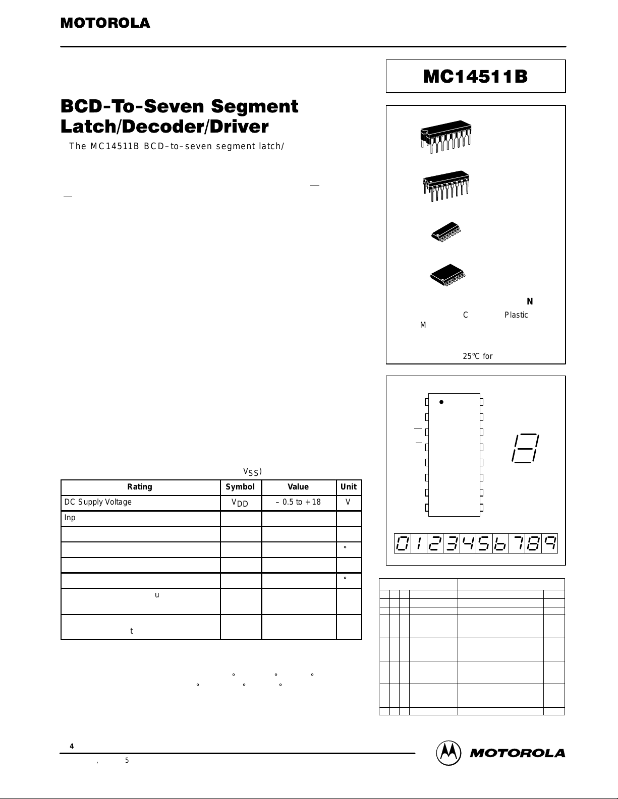
SEMICONDUCTOR TECHNICAL DATA
Motorola, Inc. 1995
REV 3
1/94
L SUFFIX
CERAMIC
CASE 620
ORDERING INFORMATION
MC14XXXBCP Plastic
MC14XXXBCL Ceramic
MC14XXXBDW SOIC
MC14XXXBD SOIC
TA = – 55° to 125°C for all packages.
P SUFFIX
PLASTIC
CASE 648
D SUFFIX
SOIC
CASE 751B
PIN ASSIGNMENT
DW SUFFIX
SOIC
CASE 751G
13
14
15
16
9
10
11
125
4
3
2
1
8
7
6
b
a
g
f
V
DD
e
d
c
BI
LT
C
B
V
SS
A
D
LE
0 1 2 3 4 5 6 7 8 9
DISPLAY
a
b
c
d
e
f g
ā
Depends upon the BCD code previously applied when LE = 0
TRUTH TABLE
LE BI LT D C B A a b c d e f g Display
X = Don’t Care
*
Inputs Outputs
X X 0 X X X X 1 1 1 1 1 1 1 8
X 0 1 X X X X 0 0 0 0 0 0 0 Blank
0 1 1 0 0 0 0 1 1 1 1 1 1 0 0
0 1 1 0 0 0 1 0 1 1 0 0 0 0 1
0 1 1 0 0 1 1 1 1 1 1 0 0 1 2
0 1 1 0 0 1 1 1 1 1 1 0 0 1 3
0 1 1 0 1 0 0 0 1 1 0 0 1 1 4
0 1 1 0 1 0 1 1 0 1 1 0 1 1 5
0 1 1 0 1 1 0 0 0 1 1 1 1 1 6
0 1 1 0 1 1 1 1 1 1 0 0 0 0 7
0 1 1 1 0 0 0 1 1 1 1 1 1 1 8
0 1 1 1 0 0 1 1 1 1 0 0 1 1 9
0 1 1 1 0 1 0 0 0 0 0 0 0 0 Blank
0 1 1 1 0 1 1 0 0 0 0 0 0 0 Blank
0 1 1 1 1 0 0 0 0 0 0 0 0 0 Blank
0 1 1 1 1 0 1 0 0 0 0 0 0 0 Blank
0 1 1 1 1 1 0 0 0 0 0 0 0 0 Blank
0 1 1 1 1 1 1 0 0 0 0 0 0 0 Blank
1 1 1 X X X X * *
MOTOROLA CMOS LOGIC DATAMC14511B
362
ELECTRICAL CHARACTERISTICS (Voltages Referenced to V
SS
)
V
– 55_C 25_C 125_C
Characteristic
Symbol
V
DD
Vdc
Min Max Min Typ # Max Min Max
Unit
“0” Level
Vin = VDD or 0
V
OL
5.0
10
15
—
—
—
0.05
0.05
0.05
—
—
—
0
0
0
0.05
0.05
0.05
—
—
—
0.05
0.05
0.05
Vdc
“1” Level
Vin = 0 or V
DD
V
OH
5.0
10
15
4.1
9.1
14.1
—
—
—
4.1
9.1
14.1
4.57
9.58
14.59
—
—
—
4.1
9.1
14.1
—
—
—
Vdc
“0” Level
(VO = 3.8 or 0.5 Vdc)
(VO = 8.8 or 1.0 Vdc)
(VO = 13.8 or 1.5 Vdc)
V
IL
5.0
10
15
—
—
—
1.5
3.0
4.0
—
—
—
2.25
4.50
6.75
1.5
3.0
4.0
—
—
—
1.5
3.0
4.0
Vdc
“1” Level
(VO = 0.5 or 3.8 Vdc)
(VO = 1.0 or 8.8 Vdc)
(VO = 1.5 or 13.8 Vdc)
V
IH
5.0
10
15
3.5
7.0
11
—
—
—
3.5
7.0
11
2.75
5.50
8.25
—
—
—
3.5
7.0
11
—
—
—
Vdc
5.0 4.1
—
3.9
—
3.4
—
—
—
—
—
—
—
4.1
—
3.9
—
3.4
—
4.57
4.24
4.12
3.94
3.70
3.54
—
—
—
—
—
—
4.1
—
3.5
—
3.0
—
—
—
—
—
—
—
Vdc
10 9.1
—
9.0
—
8.6
—
—
—
—
—
—
—
9.1
—
9.0
—
8.6
—
9.58
9.26
9.17
9.04
8.90
8.70
—
—
—
—
—
—
9.1
—
8.6
—
8.2
—
—
—
—
—
—
—
Vdc
15 14.1
—
14
—
13.6
—
—
—
—
—
—
—
14.1
—
14
—
13.6
—
14.59
14.27
14.18
14.07
13.95
13.70
—
—
—
—
—
—
14.1
—
13.6
—
13.2
—
—
—
—
—
—
—
Vdc
Output Drive Current
(VOL = 0.4 V) Sink
(VOL = 0.5 V)
(VOL = 1.5 V)
I
OL
5.0
10
15
0.64
1.6
4.2
—
—
—
0.51
1.3
3.4
0.88
2.25
8.8
—
—
—
0.36
0.9
2.4
—
—
—
mAdc
Input Current I
in
15 — ± 0.1 — ±0.00001 ± 0.1 — ± 1.0 µAdc
Input Capacitance C
in
— — — — 5.0 7.5 — — pF
Quiescent Current
(Per Package) Vin = 0 or VDD,
I
out
= 0 µA
I
DD
5.0
10
15
—
—
—
5.0
10
20
—
—
—
0.005
0.010
0.015
5.0
10
20
—
—
—
150
300
600
µAdc
Total Supply Current**†
(Dynamic plus Quiescent,
Per Package)
(CL = 50 pF on all outputs, all
buffers switching)
I
T
5.0
10
15
IT = (1.9 µA/kHz) f + I
DD
IT = (3.8 µA/kHz) f + I
DD
IT = (5.7 µA/kHz) f + I
DD
µAdc
#Noise immunity specified for worst–case input combination.
Noise Margin for both “1” and “0” level =
1.0 Vdc min @ VDD = 5.0 Vdc
2.0 Vdc min @ VDD = 10 Vdc
2.5 Vdc min @ VDD = 15 Vdc
**āThe formulas given are for the typical characteristics only at 25_C.
†To calculate total supply current at loads other than 50 pF:
IT(CL) = IT(50 pF) + 3.5 x 10⁻³ (CL – 50) VDDf
where: IT is in µA (per package), CL in pF, VDD in Vdc, and f in kHz is input frequency.
Output Voltage
Input Voltage #
Output Drive Voltage
(IOH = 0 mA) Source
(IOH = 5.0 mA)
(IOH = 10 mA)
(IOH = 15 mA)
(IOH = 20 mA)
(IOH = 25 mA)
(IOH = 0 mA)
(IOH = 5.0 mA)
(IOH = 10 mA)
(IOH = 15 mA)
(IOH = 20 mA)
(IOH = 25 mA)
(IOH = 0 mA)
(IOH = 5.0 mA)
(IOH = 10 mA)
(IOH = 15 mA)
(IOH = 20 mA)
(IOH = 25 mA)
V
OH
MOTOROLA CMOS LOGIC DATA
363
MC14511B
SWITCHING CHARACTERISTICS* (C
L
= 50 pF, TA = 25_C)
Characteristic
Symbol
V
DD
Vdc
Min Typ Max Unit
Output Rise Time
t
TLH
= (0.40 ns/pF) CL + 20 ns
t
TLH
= (0.25 ns/pF) CL + 17.5 ns
t
TLH
= (0.20 ns/pF) CL + 15 ns
t
TLH
5.0
10
15
—
—
—
40
30
25
80
60
50
ns
Output Fall Time
t
THL
= (1.5 ns/pF) CL + 50 ns
t
THL
= (0.75 ns/pF) CL + 37.5 ns
t
THL
= (0.55 ns/pF) CL + 37.5 ns
t
THL
5.0
10
15
—
—
—
125
75
65
250
150
130
ns
t
PLH
5.0
10
15
—
—
—
640
250
175
1280
500
350
t
PHL
5.0
10
15
—
—
—
720
290
200
1440
580
400
t
PLH
5.0
I0
15
—
—
—
600
200
150
750
300
220
t
PHL
5.0
10
15
—
—
—
485
200
160
970
400
320
t
PLH
5.0
10
15
—
—
—
313
125
90
625
250
180
t
PHL
5.0
10
15
—
—
—
313
125
90
625
250
180
Setup Time t
su
5.0
10
15
100
40
30
—
—
—
—
—
—
ns
Hold Time t
h
5.0
10
15
60
40
30
—
—
—
—
—
—
ns
Latch Enable Pulse Width t
WL
5.0
10
15
520
220
130
260
110
65
—
—
—
ns
*The formulas given are for the typical characteristics only.
This device contains protection circuitry to protect the inputs against damage due to high static voltages or electric fields; however, it is advised that normal precautions be taken to avoid application of any voltage higher than maximum rated voltages to this
high-impedance circuit. A destructive high current mode may occur if Vin and V
out
are not constrained to the range VSS ≤ (Vin or
V
out
) ≤ VDD.
Due to the sourcing capability of this circuit, damage can occur to the device if VDD is applied, and the outputs are shorted to
VSS and are at a logical 1 (See Maximum Ratings).
Unused inputs must always be tied to an appropriate logic voltage level (e.g., either VSS or VDD).
Data Propagation Delay Time
t
= (0.40 ns/pF) CL + 620 ns
PLH
t
= (0.25 ns/pF) CL + 237.5 ns
PLH
t
= (0.20 ns/pF) CL + 165 ns
PLH
t
= (1.3 ns/pF) CL + 655 ns
PHL
t
= (0.60 ns/pF) CL + 260 ns
PHL
t
= (0.35 ns/pF) CL + 182.5 ns
PHL
Blank Propagation Delay Time
t
= (0.30 ns/pF) CL + 585 ns
PLH
t
= (0.25 ns/pF) CL + 187.5 ns
PLH
t
= (0.15 ns/pF) CL + 142.5 ns
PLH
t
= (0.85 ns/pF) CL + 442.5 ns
PHL
t
= (0.45 ns/pF) CL + 177.5 ns
PHL
t
= (0.35 ns/pF) CL + 142.5 ns
PHL
Lamp Test Propagation Delay Time
t
= (0.45 ns/pF) CL + 290.5 ns
PLH
t
= (0.25 ns/pF) CL + 112.5 ns
PLH
t
= (0.20 ns/pF) CL + 80 ns
PLH
t
= (1.3 ns/pF) CL + 248 ns
PHL
t
= (0.45 ns/pF) CL + 102.5 ns
PHL
t
= (0.35 ns/pF) CL + 72.5 ns
PHL
ns
ns
ns
 Loading...