

SEMICONDUCTOR TECHNICAL DATA
CMOS
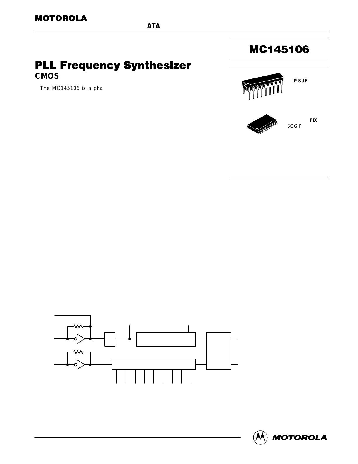
The MC145106 is a phase–locked loop (PLL) frequency synthesizer
constructed in CMOS on a single monolithic structure. This synthesizer finds
applications in such areas as CB and FM transceivers. The device contains an
oscillator/amplifier, a 210 or 211 divider chain for the oscillator signal, a
programmable divider chain for the input signal, and a phase detector. The
MC145106 has circuitry for a 10.24 MHz oscillator or may operate with an
external signal. The circuit provides a 5.12 MHz output signal, which can be
used for frequency tripling. A 29 programmable divider divides the input signal
frequency for channel selection. The inputs to the programmable divider are
standard ground–to–supply binary signals. Pull–down resistors on these inputs
normally set these inputs to ground enabling these programmable inputs to be
controlled from a mechanical switch or electronic circuitry.
The phase detector may control a VCO and yields a high level signal when
input frequency is low, and a low level signal when input frequency is high. An
out–of–lock signal is provided from the on–chip lock detector with a “0” level for
the out–of–lock condition.
• Single Power Supply
• Wide Supply Range: 4.5 to 12 V
• Provision for 10.24 MHz Crystal Oscillator
• 5.12 MHz Output
• Programmable Division Binary Input Selects up to 2
• On–Chip Pull–Down Resistors on Programmable Divider Inputs
• Selectable Reference Divider, 210 or 211 (Including ÷ 2)
• Three–State Phase Detector
• See Application Note AN535 and Article Reprint AR254
• Chip Complexity: 880 FETs or 220 Equivalent Gates
• See the MC145151–2 and MC145152–2 for Higher Performance and
Added Flexibility
9
Order this document
by MC145106/D
P SUFFIX
PLASTIC DIP
18
1
20
1
ORDERING INFORMATION
MC145106P Plastic DIP
MC145106DW SOG Package
CASE 707
DW SUFFIX
SOG PACKAGE
CASE 751D
BLOCK DIAGRAM
OSC
out
÷
2
out
÷
OSC
in
f
in
REV 3
1/98
Motorola, Inc. 1998
MC145106 MOTOROLA
2
DIVIDE–BY–N COUNTER 29 – 1
P0 P1 P2 P3 P4 P5 P6 P7 P8
REFERENCE
DIVIDE 29 OR 2
10
FS
PHASE
DETECTOR
φ
LD
Det
out
1
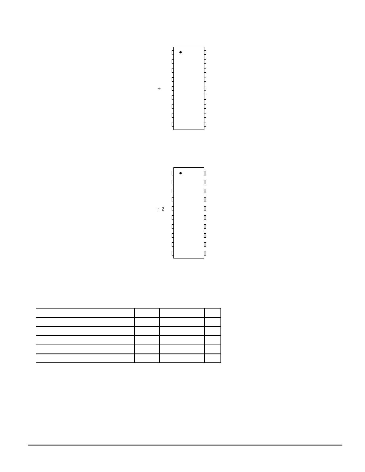
PIN ASSIGNMENTS
PLASTIC DIP
V
1
DD
f
2
in
OSC
OSC
B
φ
Det
3
in
4
out
2
5
out
FS
6
7
out
LD
8
P8
9
SOG PACKAGE
18
17
16
15
14
13
12
11
10
V
P0
P1
P2
P3
P4
P5
P6
P7
SS
V
1
DD
f
2
in
OSC
OSC
B
φ
Det
MAXIMUM RATINGS (Voltages Referenced to V
Parameter Symbol Value Unit
DC Supply Voltage V
Input Voltage, All Inputs V
DC Input Current, per Pin I ± 10 mA
Operating Temperature Range T
Storage Temperature Range T
SS
DD
in
A
stg
)
3
in
4
out
2
5
out
6
FS
7
out
LD
8
P8
9
P7
10
NC = NO CONNECTION
– 0.5 to + 12 V
– 0.5 to VDD + 0.5 V
– 40 to + 85 °C
– 65 to + 150 °C
20
19
18
17
16
15
14
13
12
11
V
P0
NC
P1
P2
P3
P4
NC
P5
P6
SS
This device contains circuitry to protect the
inputs against damage due to high static voltages or electric fields; however, it is advised that
normal precautions be taken to avoid application
of any voltage higher than maximum rated
voltages to this high impedance circuit. For
proper operation it is recommended that Vin and
V
be constrained to the range VSS ≤ (Vin or
out
V
) ≤ VDD.
out
MC145106MOTOROLA
2
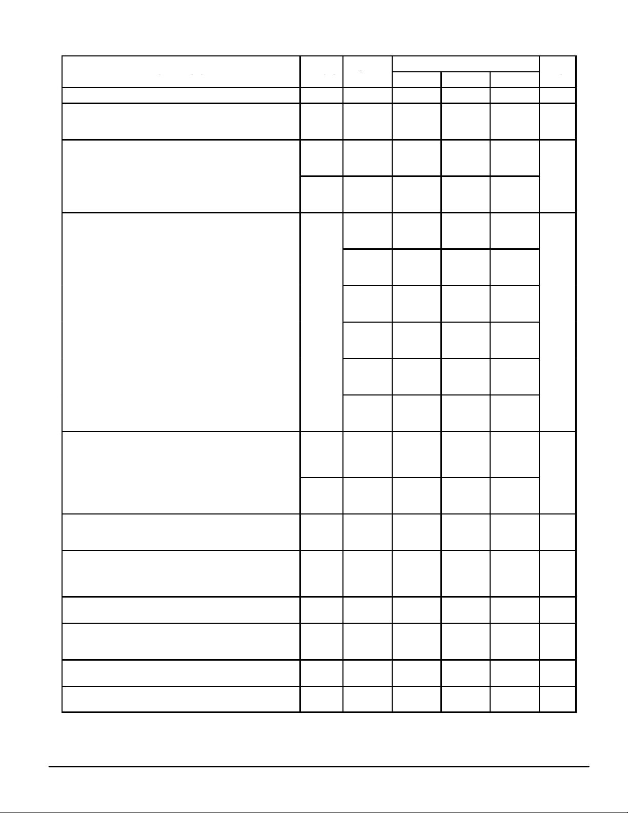
ELECTRICAL CHARACTERISTICS (T
V
DD
Characteristic Symbol
Power Supply Voltage Range V
Supply Current I
Input Voltage “0” Level V
Input Current “0” Level
FS, Pull–Up Resistor Source Current)
(P0 – P8) 5.0
(FS) “1” Level 5.0
(P0 – P8, Pull–Down Resistor Sink Current) 5.0
(OSCin, fin) “0” Level 5.0
(OSCin, fin) “1” Level 5.0
Output Drive Current
(VO = 4.5 V) Source
(VO = 9.5 V)
(VO = 11.5 V)
(VO = 0.5 V) Sink
(VO = 0.5 V)
(VO = 0.5 V)
Input Amplitude
(fin @ 4.0 MHz)
(OSCin @ 10.24 MHz)
Input Resistance
(OSCin, fin)
Input Capacitance
(OSCin, fin)
Three–State Leakage Current
(φDet
Input Frequency
(– 40 to + 85°C)
Oscillator Frequency
(– 40 to + 85°C)
*Data labelled “Typ” is not to be used for design purposes but is intended as an indication of the IC’s potential performance.
out
)
= 25°C Unless Otherwise Stated, Voltages Referenced to VSS)
A
V
“1” Level V
OSC
I
I
R
C
I
DD
DD
IL
IH
I
in
OH
OL
—
in
in
OZ
f
in
Vdc
— 4.5 — 12 V
5.0
10
12
5.0
10
12
5.0
10
12
5.0
10
12
10
12
10
12
10
12
10
12
10
12
5.0
10
12
5.0
10
12
—
—
5.0
10
12
— — 6.0 — pF
5.0
10
12
4.5
12
in
4.5
12
Min Typ* Max
—
—
—
—
—
—
3.5
7.0
8.4
– 5.0
– 15
– 20
—
—
—
—
—
—
7.5
22.5
30
– 2.0
– 6.0
– 9.0
2.0
6.0
9.0
– 0.7
– 1.1
– 1.5
0.9
1.4
2.0
1.0
1.5
—
—
—
—
—
—
0
0
0.1
0.1
All Types
6
20
28
—
—
—
—
—
—
– 20
– 60
– 80
—
—
—
—
—
—
30
90
120
– 6.0
– 25
– 37
6.0
25
37
– 1.4
– 2.2
– 3.0
1.8
2.8
4.0
0.2
0.3
1.0
0.5
—
—
—
—
—
—
—
—
10
35
50
1.5
3.0
3.6
—
—
—
– 50
– 150
– 200
– 0.3
– 0.3
– 0.3
0.3
0.3
0.3
75
225
300
– 15
– 62
– 92
15
62
92
—
—
—
—
—
—
—
—
—
—
—
1.0
1.0
1.0
4.0
4.0
10.24
10.24
Unit
mA
V
µA
mA
V p–p
Sine
MΩ
µA
MHz
MHz
MC145106 MOTOROLA
3
 Loading...