

Motorola MC14508BCL, MC14508BCP, MC14508BDW Datasheet
MOTOROLA CMOS LOGIC DATAMC14508B
344
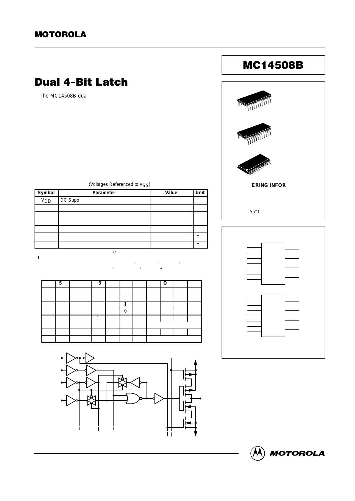
The MC14508B dual 4–bit latch is constructed with MOS P–channel and
N–channel enhancement mode devices in a single monolithic structure. The
part consists of two identical, independent 4–bit latches with separate Strobe
(ST) and Master Reset (MR) controls. Separate Disable inputs force the
outputs to a high impedance state and allow the devices to be used in time
sharing bus line applications.
These complementary MOS latches find primary use in buffer storage,
holding register, o r general digital logic functions where low power
dissipation and/or high noise immunity is desired.
• 3–State Output
• Supply Voltage Range = 3.0 Vdc to 18 Vdc
• Capable–of Driving Two Low–power TTL Loads or One Low–power
Schottky TTL Load over the Rated Temperature Range
MAXIMUM RATINGS* (Voltages Referenced to V
SS
)
Symbol
Parameter Value Unit
V
DD
DC Supply Voltage – 0.5 to + 18.0 V
Vin, V
out
Input or Output Voltage (DC or Transient) – 0.5 to VDD + 0.5 V
Iin, I
out
Input or Output Current (DC or Transient),
per Pin
± 10 mA
P
D
Power Dissipation, per Package† 500 mW
T
stg
Storage Temperature – 65 to + 150
_
C
T
L
Lead Temperature (8–Second Soldering) 260
_
C
*Maximum Ratings are those values beyond which damage to the device may occur.
†Temperature Derating:
Plastic “P and D/DW” Packages: – 7.0 mW/_C From 65_C To 125_C
Ceramic “L” Packages: – 12 mW/_C From 100_C To 125_C
TRUTH TABLE
MR ST Disable D3 D2 D1 D0 Q3 Q2 Q1 Q0
0 1 0 0 0 0 0 0 0 0 0
0 1 0 0 0 0 1 0 0 0 1
0 1 0 0 0 1 0 0 0 1 0
0 1 0 0 1 0 0 0 1 0 0
0 1 0 1 0 0 0 1 0 0 0
0 0 0 X X X X Latched
1 X 0 X X X X 0 0 0 0
X X 1 X X X X High Impedance
X = Don’t Care
CIRCUIT DIAGRAM
DIS
MR
ST
D
n
(TO OTHER THREE LATCHES)
V
DD
Q
n
V
SS
SEMICONDUCTOR TECHNICAL DATA
Motorola, Inc. 1995
REV 3
1/94
L SUFFIX
CERAMIC
CASE 623
ORDERING INFORMATION
MC14XXXBCP Plastic
MC14XXXBCL Ceramic
MC14XXXBDW SOIC
TA = – 55° to 125°C for all packages.
P SUFFIX
PLASTIC
CASE 709
DW SUFFIX
SOIC
CASE 751E
BLOCK DIAGRAM
22
20
18
16
15
14
13
10
8
6
4
3
2
1
23
21
19
17
11
9
7
5
MR
ST
DIS
D0
D1
D2
D3
MR
ST
DIS
D0
D1
D2
D3
Q0
Q1
Q2
Q3
Q0
Q1
Q2
Q3
VDD = PIN 24
VSS = PIN 12
MOTOROLA CMOS LOGIC DATA
345
MC14508B
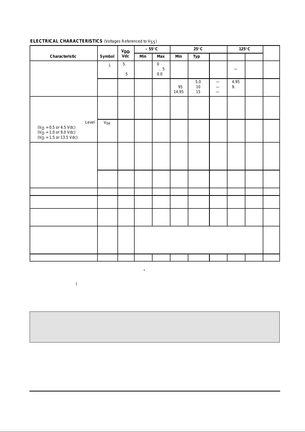
ELECTRICAL CHARACTERISTICS (Voltages Referenced to V
SS
)
V
– 55_C 25_C 125_C
Characteristic
Symbol
V
DD
Vdc
Min Max Min Typ # Max Min Max
Unit
Output Voltage
“0” Level
Vin = VDD or 0
V
OL
5.0
10
15
—
—
—
0.05
0.05
0.05
—
—
—
0
0
0
0.05
0.05
0.05
—
—
—
0.05
0.05
0.05
Vdc
“1” Level
Vin = 0 or V
DD
V
OH
5.0
10
15
4.95
9.95
14.95
—
—
—
4.95
9.95
14.95
5.0
10
15
—
—
—
4.95
9.95
14.95
—
—
—
Vdc
Input Voltage
“0” Level
(VO = 4.5 or 0.5 Vdc)
(VO = 9.0 or 1.0 Vdc)
(VO = 13.5 or 1.5 Vdc)
V
IL
5.0
10
15
—
—
—
1.5
3.0
4.0
—
—
—
2.25
4.50
6.75
1.5
3.0
4.0
—
—
—
1.5
3.0
4.0
Vdc
“1” Level
(VO = 0.5 or 4.5 Vdc)
(VO = 1.0 or 9.0 Vdc)
(VO = 1.5 or 13.5 Vdc)
V
IH
5.0
10
15
3.5
7.0
11
—
—
—
3.5
7.0
11
2.75
5.50
8.25
—
—
—
3.5
7.0
11
—
—
—
Vdc
Output Drive Current
(VOH = 2.5 Vdc) Source
(VOH = 4.6 Vdc)
(VOH = 9.5 Vdc)
(VOH = 13.5 Vdc)
I
OH
5.0
5.0
10
15
– 3.0
– 0.64
– 1.6
– 4.2
—
—
—
—
– 2.4
– 0.51
– 1.3
– 3.4
– 4.2
– 0.88
– 2.25
– 8.8
—
—
—
—
– 1.7
– 0.36
– 0.9
– 2.4
—
—
—
—
mAdc
(VOL = 0.4 Vdc) Sink
(VOL = 0.5 Vdc)
(VOL = 1.5 Vdc)
I
OL
5.0
10
15
0.64
1.6
4.2
—
—
—
0.51
1.3
3.4
0.88
2.25
8.8
—
—
—
0.36
0.9
2.4
—
—
—
mAdc
Input Current I
in
15 — ± 0.1 — ±0.00001 ± 0.1 — ± 1.0 µAdc
Input Capacitance
(Vin = 0)
C
in
— — — — 5.0 7.5 — — pF
Quiescent Current
(Per Package)
I
DD
5.0
10
15
—
—
—
5.0
10
20
—
—
—
0.005
0.010
0.015
5.0
10
20
—
—
—
150
300
600
µAdc
Total Supply Current**†
(Dynamic plus Quiescent,
Per Package)
(CL = 50 pF on all outputs, all
buffers switching)
I
T
5.0
10
15
IT = (1.46 µA/kHz) f + I
DD
IT = (2.91 µA/kHz) f + I
DD
IT = (4.37 µA/kHz) f + I
DD
µAdc
Three–State Leakage Current I
TL
15 — ± 0.1 — ± 0.0001 ± 0.1 — ± 3.0 µAdc
#Data labelled “Typ” is not to be used for design purposes but is intended as an indication of the IC’s potential performance.
**āThe formulas given are for the typical characteristics only at 25_C.
†To calculate total supply current at loads other than 50 pF:
IT(CL) = IT(50 pF) + (CL – 50) Vfk
where: IT is in µA (per package), CL in pF, V = (VDD – VSS) in volts, f in kHz is input frequency, and k = 0.008.
This device contains protection circuitry to guard against damage due to high static voltages or electric fields. However,
precautions must be taken to avoid applications of any voltage higher than maximum rated voltages to this high-impedance
circuit. For proper operation, Vin and V
out
should be constrained to the range VSS ≤ (Vin or V
out
) ≤ VDD.
Unused inputs must always be tied to an appropriate logic voltage level (e.g., either VSS or VDD). Unused outputs must
be left open.
MOTOROLA CMOS LOGIC DATAMC14508B
346
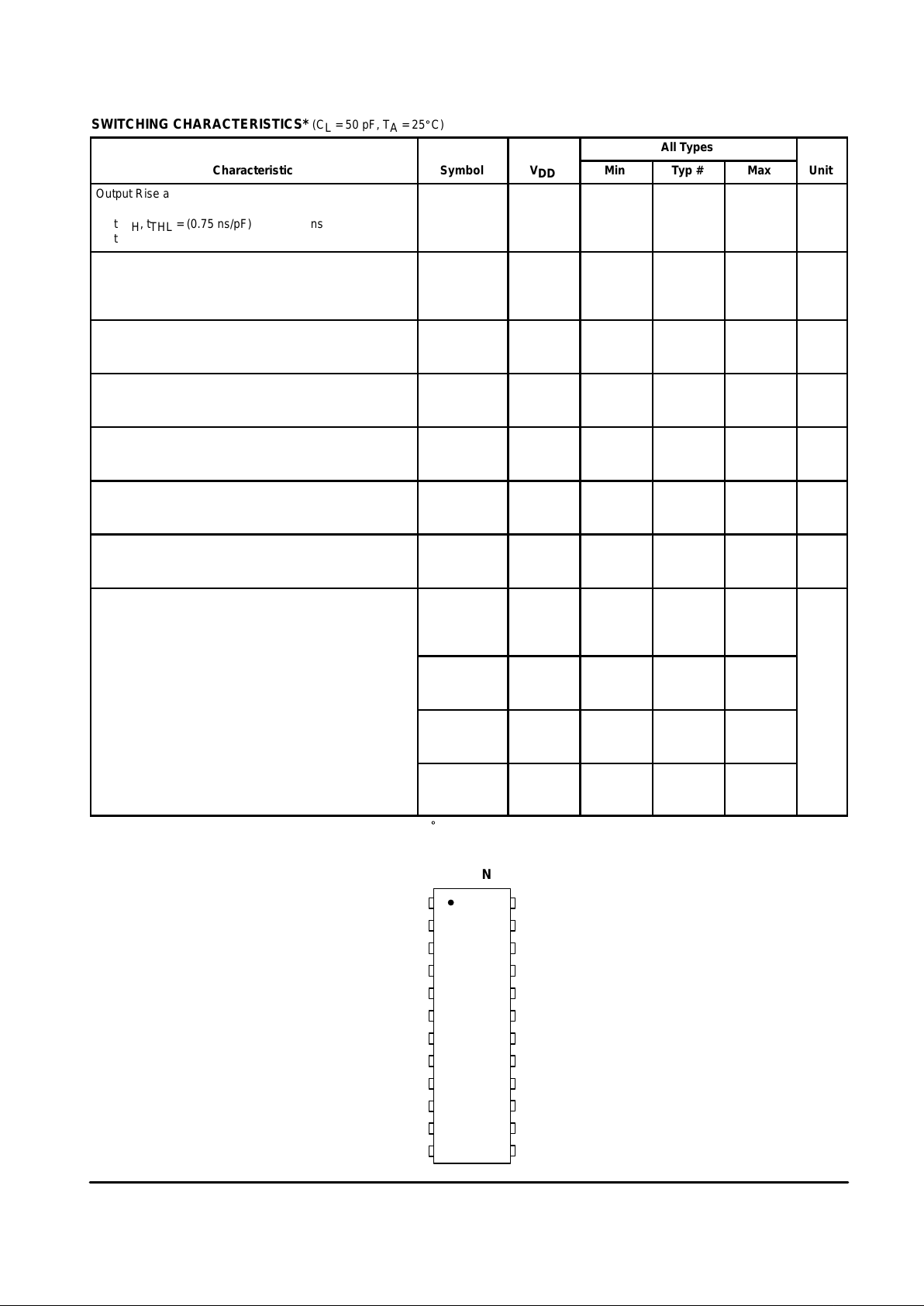
SWITCHING CHARACTERISTICS* (C
L
= 50 pF, TA = 25_C)
All Types
Characteristic
Symbol
V
DD
Min Typ # Max
Unit
Output Rise and Fall Time
t
TLH
, t
THL
= (1.5 ns/pF) CL + 25 ns
t
TLH
, t
THL
= (0.75 ns/pF) CL + 12.5 ns
t
TLH
, t
THL
= (0.55 ns/pF) CL + 9.5 ns
t
TLH
, t
THL
5.0
10
15
—
—
—
100
50
40
200
100
80
ns
Propagation Delay Time, Dn or MR to Q
t
PLH
, t
PHL
= (1.7 ns/pF) CL + 135 ns
t
PLH
, t
PHL
= (0.66 ns/pF) CL + 57 ns
t
PLH
, t
PHL
= (0.5 ns/pF) CL + 35 ns
t
PLH
, t
PHL
5.0
10
15
—
—
—
220
90
60
440
180
120
ns
Master Reset Pulse Width t
WH(R)
5.0
10
15
200
100
70
100
50
35
—
—
—
ns
Master Reset Removal Time t
rem
5.0
10
15
30
25
20
– 15
0
0
—
—
—
ns
Strobe Pulse Width t
WH(S)
5.0
10
15
140
70
40
70
35
20
—
—
—
ns
Setup Time
Data to Strobe
t
su
5.0
10
15
50
20
10
25
10
5.0
—
—
—
ns
Hold Time
Strobe to Data
t
h
5.0
10
15
50
35
35
20
10
10
—
—
—
ns
3–State Propagation Delay Time
Output “1” to High Impedance
t
PHZ
5.0
10
15
—
—
—
55
35
30
170
100
70
ns
Output “0” to High Impedance t
PLZ
5.0
10
15
—
—
—
75
40
35
170
100
70
High Impedance to “1” Level t
PZH
5.0
10
15
—
—
—
80
35
30
170
100
70
High Impedance to “0” Level t
PZL
5.0
10
15
—
—
—
105
50
35
210
100
70
*The formulas given are for the typical characteristics only at 25_C.
#Data labelled “Typ” is not to be used for design purposes but is intended as an indication of the IC’s potential performance.
PIN ASSIGNMENT
D1
A
D0
A
DIS
A
ST
A
MR
A
D2
A
Q1
A
Q0
A
D2
B
Q2
B
D3
B
Q3
B
V
DD
DIS
B
D0
B
Q0
B
5
4
3
2
1
10
9
8
7
6
14
15
16
17
18
19
20
13
11
12
21
22
23
24
MR
B
ST
B
D1
B
Q1
B
Q3
A
V
SS
D3
A
Q2
A
 Loading...