MC145076
MOTOROLA
1
Product Preview
CMOS
The MC145076 is a combination re–clocking and smoothing filter designed
especially for the MC145074 Stereo Audio DAC. Its versatility however, allows
it to be used with any single bit–stream data converter to provide output
reconstruction filtering, and to improve performance by restoring pulse shape
integrity. The MC145076 provides a well controlled, filtered output that can be
used directly, or with a current summing operational amplifier.
The MC145076 is intended to be one half of a two–chip solution for serial bit
steam DACs. The analog filtering function of the MC145076 eases the digital
filtering requirements at the input to the digital noise shaping modulator, and
eliminates the need for precision analog output filtering capacitors, resulting in
lower overall system cost. The MC145076 pulse shape restoration frees the
designer from analog pitfalls that can impact performance, thereby lowering the
risk of new product development with a sigma–delta DAC.
• Single–Ended Stereo Outputs Require no Additional Smoothing Filters
• 86 dB S/D, 96 dB S/N with MC145074 @ 192 x OSR Single Ended
• > 100 dB S/(N+D) @ 256 OSR, Differential Mode
• 18.5 MHz Maximum Serial Data Input Rate
• – 80 dB Cross Channel Interference
• 72–Tap FIR with > 40 dB Alias Filtering
• Operating Temperature Range: – 40 to + 85_C
• Buffered Data Clock Output for Ease of Data Generation
• 16–Pin Narrow Body SOIC Package
• Single Supply Operation: + 5 V
TIMING
AND
CONTROL
LOGIC
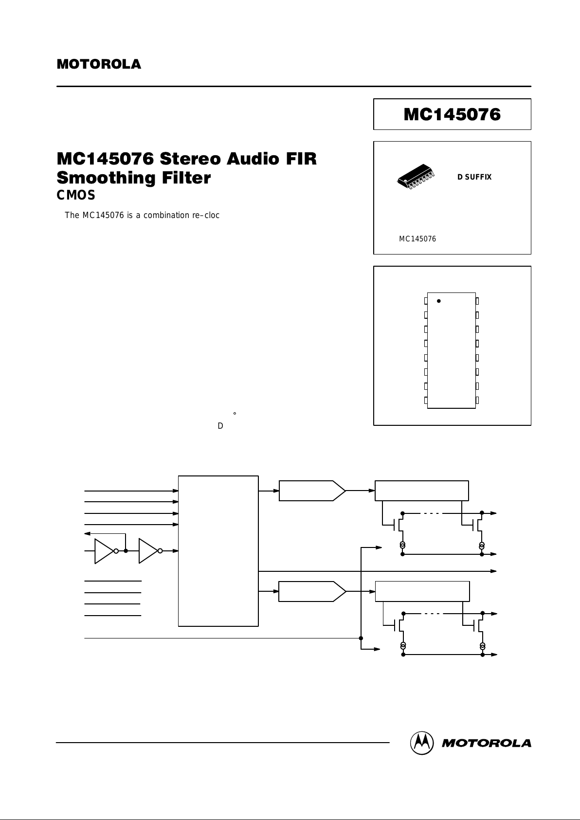
DIL
5
DIR
6
DIV2
4
TEST
7
X
out
X
in
16
2
V
DDA
1
V
DDD
8
GND
10
GND
15
LEFT 144 SERIAL SHIFT REG.
LEFT CHOP
C (1)
14
IOL
GND
144 TAP HAMMING
WINDOW
COEFFICIENTS
13
9
CLKOUT
RIGHT 144 SERIAL SHIFT REG.
RIGHT CHOP
C (1)
11
IOR
GND
144 TAP HAMMING
WINDOW
COEFFICIENTS
12
C (144)
C (144)
BIAS
3
This document contains information on a product under development. Motorola reserves the right to change or discontinue this product without notice.
Order this document
by MC145076/D
SEMICONDUCTOR TECHNICAL DATA
PIN ASSIGNMENT
D SUFFIX
16–PIN SOG
CASE 751B–05
ORDERING INFORMATION
MC145076D SOG Package
13
14
15
16
9
10
11
125
4
3
2
1
8
7
6
GND
GND
IOL
GND
X
out
CLKOUT
GND
IOR
DIV2
BIAS
X
in
V
DDA
V
DDD
TEST
DIR
DIL
16
1
Motorola, Inc. 1996
REV 1
9/96

MC145076
MOTOROLA
2
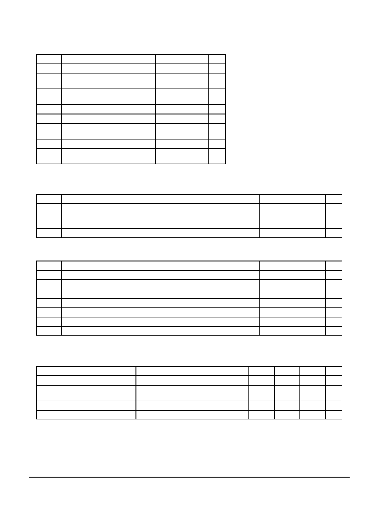
MAXIMUM RATINGS*
Symbol Parameter Value Unit
V
DD
DC Supply Voltage (Referenced to GND) 6.0 V
V
in
DC Input Voltage
GND
– 0.5 to
VDD + 0.5
V
V
out
DC Output Voltage GND – 0.5 to
VDD + 0.5
V
I
in
DC Input Current, per Pin ± 10 mA
I
out
DC Output Current, per Pin ± 20 mA
IDD,
I
GND
DC Supply Current, VDD and GND Pins ± 60 mA
T
stg
Storage Temperature – 55 to 150 °C
T
L
Lead Temperature, 1 mm from Case for
10 Seconds
260 °C
*Maximum Ratings are those values beyond which damage to the device may occur . Func-
tional operation should be restricted to the Operation Ranges below.
OPERATION RANGES (Applicable to Guaranteed Limits)
Symbol
Parameter Value Unit
V
DD
DC Supply Voltage 4.5 to 5.5 V
V
IOL
,
V
IOR
IOL, IOR Virtual Ground VDD – 2.0 to V
DD
V
T
A
Ambient Operating Temperature – 40 to + 85 °C
DC ELECTRICAL CHARACTERISTICS
(Voltages Referenced to GND, Full Temperature and Voltage Ranges per Operation Ranges Table, unless otherwise indicated)
Symbol
Parameter Guaranteed Limit Unit
V
IH
Minimum High–Level Input Voltage 0.7 x V
DD
V
V
IL
Maximum Low–Level Input Voltage 0.3 x V
DD
V
V
OH
Minimum High–Level Output Voltage IOH = 0.4 mA VDD – 0.3 V
V
OL
Maximum Low–Level Output Voltage IOL = 0.4 mA GND + 0.3 V
I
DD
Maximum Power Supply Current R
bias
= 4640 Ω 40 mA
IOL, I
OR
Left/Right Channel Output Current* 2 ± 20% mA
I
lkg
Input Leakage Current ± 10 µA
*50% Duty Cycle, V
DDA
= 5 V, R
bias
= 4640 Ω
SINGLE ENDED ANALOG CHARACTERISTICS
(Xin = 16.9344 MHz, DIV2 = 0, fin = 990.527 Hz, 20 Bit 2nd Order Modulator Input Data)
Parameter
Test Conditions Min Typ Max Unit
Dynamic Range S/(N+D) @ – 60 dB input, + 60 dB — 96 — dB
S/(N+D) Flat
A–weighted
(– 6 dB) 25 to 75% peak to peak input duty cycle
(– 20 dB)
86
—
90
80*
— dB
Idle Channel Noise CLKOUT/4 digital input data pattern — 105 — dB
60 Hz Power Supply Rejection With 47 µF and 4640 Ω on Bias Pin — 40 — dB
*Noise performance limited by second order digital modulator .
This device contains protection circuitry to
guard against damage due to high static voltages or electric fields. However, precautions
must be taken to avoid applications of any voltage higher than maximum rated voltages to
this high–impedance circuit. For proper operation, Vin and V
out
should be constrained to the
range GND ≤ (Vin or V
out
) ≤ VDD.
Unused inputs must always be tied to an
appropriate logic voltage level (e.g., either
GND or VDD). Unused outputs must be left
open.

MC145076
MOTOROLA
3
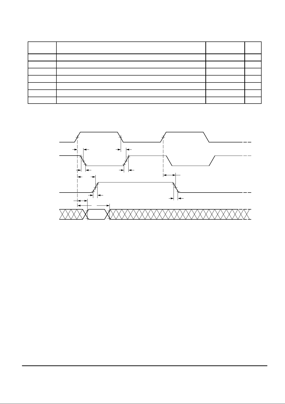
AC ELECTRICAL CHARACTERISTICS (Full Temperature and Voltage Ranges per Operation Ranges Table)
Symbol
Parameter
Guaranteed
Limit
Unit
f Clock Frequency, X
in
37 MHz
t
PLH
, t
PHL
Maximum Propagation Delay, Xin to X
out
5 ns
t
TLH
, t
THL
Maximum Rise/Fall Time, X
out
10 ns
t
PLH
, t
PHL
Maximum Propagation Delay, Xin to CLKOUT 30 ns
t
TLH
, t
THL
Maximum Rise/Fall Time, CLKOUT 10 ns
t
su
Minimum DIR, DIL Setup Time From X
in
5 ns
t
h
Maximum DIR, DIL Hold Time From X
in
20 ns
NOTE: 10 pF load capacitance, Xin rise and fall times set at 2 ns.
TIMING WAVEFORMS
X
in
50%
t
su
t
PHL
X
out
CLKOUT
50%
10%
50%
90%
10%
50%
50% 50%
t
PLH
t
TLH
t
THL
t
TLH
t
THL
t
PLH
t
PHL
t
h
90%
90%
10%
10%
90%
50%
90%
10%
DIR OR DIL
Figure 1.
 Loading...