Motorola MC145074D Datasheet

MC145074
1
MOTOROLA
Product Preview
CMOS
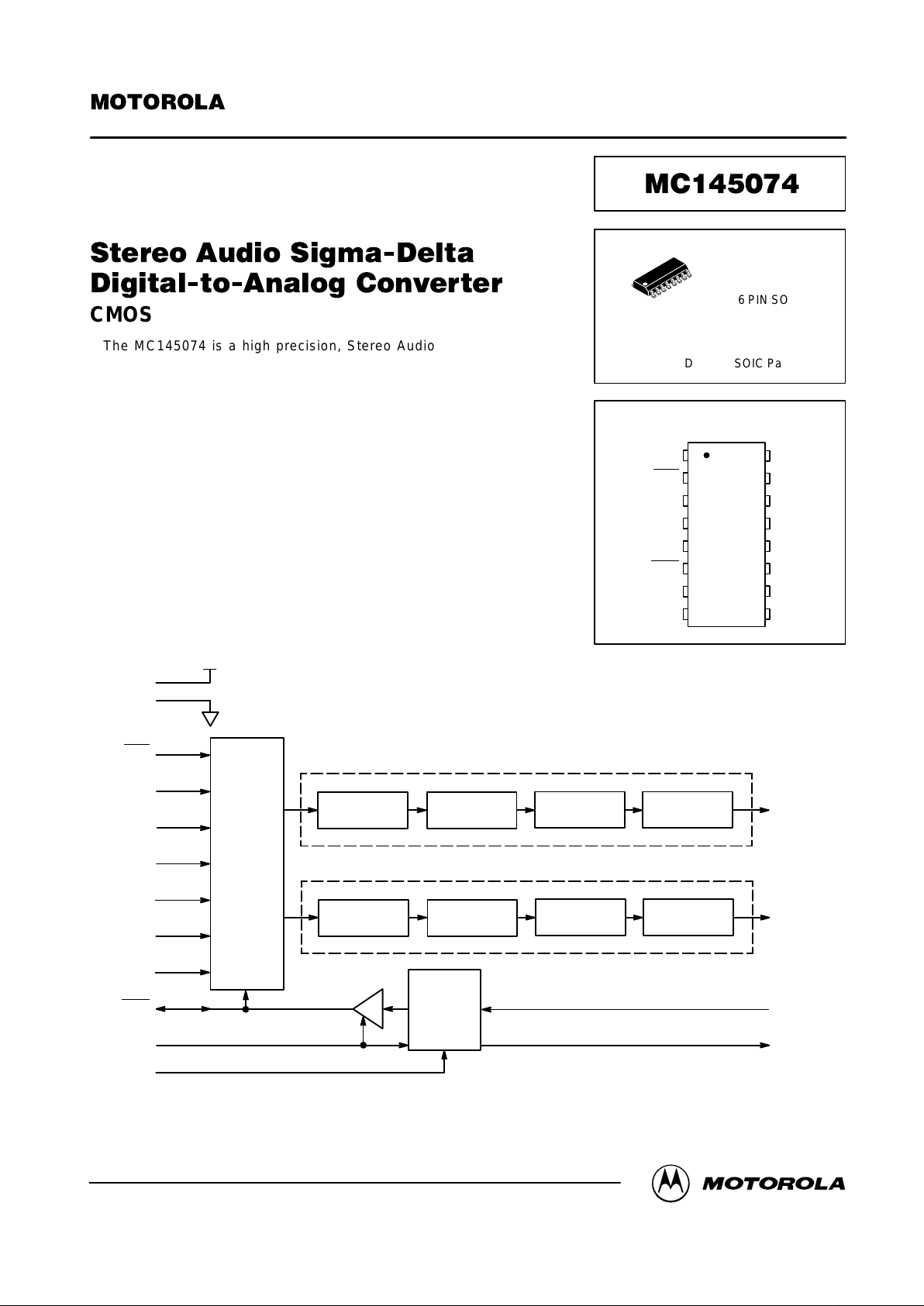
The MC145074 is a high precision, Stereo Audio Digital–to–Analog
Converter that utilizes second order sigma–delta modulators with 2–tap FIR
feedback architecture. The part can be used as a stand alone stereo digital
modulator, or as a companion part to the MC145076 smoothing filter to achieve
high quality, low cost audio performance.
• Peak S/(N+D) > 100 dB
• Single 5 V Supply Operation
• Accepts 16, 18, or 20–Bit Data Words
• Dual/Single Pin Data Input Modes
• Programmable WCLK Divider
• Operating Temperature Range: – 40 to + 85°C
• Low Power Consumption: 40 mW Typical
• Companion to MC145076 Stereo Audio FIR Smoothing Filter
2
STBY
DIL/WDL Y
DIR/DILR
BCLK
DMODE
RES1
RES0
3
4
5
13
14
15
CONTROL
LOGIC
SERIAL/P ARALLEL
INTERFACE
OFFSET SCALER
Σ ± ∆
MODULA TOR
CHOP
DOL
DOR
16
SERIAL/P ARALLEL
INTERFACE
OFFSET SCALER
Σ ± ∆
MODULA TOR
CHOP
9
6
WCLK
TIMING
MSTR
DIV2
7
X
out
X
in
12
11
8
1
V
DD
V
SS
LEFT CHANNEL
RIGHT CHANNEL
10
This document contains information on a product under development. Motorola reserves the right to change or discontinue this product without notice.
Order this document
by MC145074/D
SEMICONDUCTOR TECHNICAL DATA
PIN ASSIGNMENT
D SUFFIX
16 PIN SOIC
CASE 751B–05
ORDERING INFORMATION
MC145074D SOIC Package
13
14
15
16
9
10
11
125
4
3
2
1
8
7
6
X
in
DMODE
RES1
RES0
DOL
DOR
DIV2
X
out
DIR/DILR
DIL/WDL Y
STBY
V
SS
MSTR
WCLK
BCLK
V
DD
16
1
Motorola, Inc. 1996
REV 1
5/96

MC145074
MOTOROLA
2
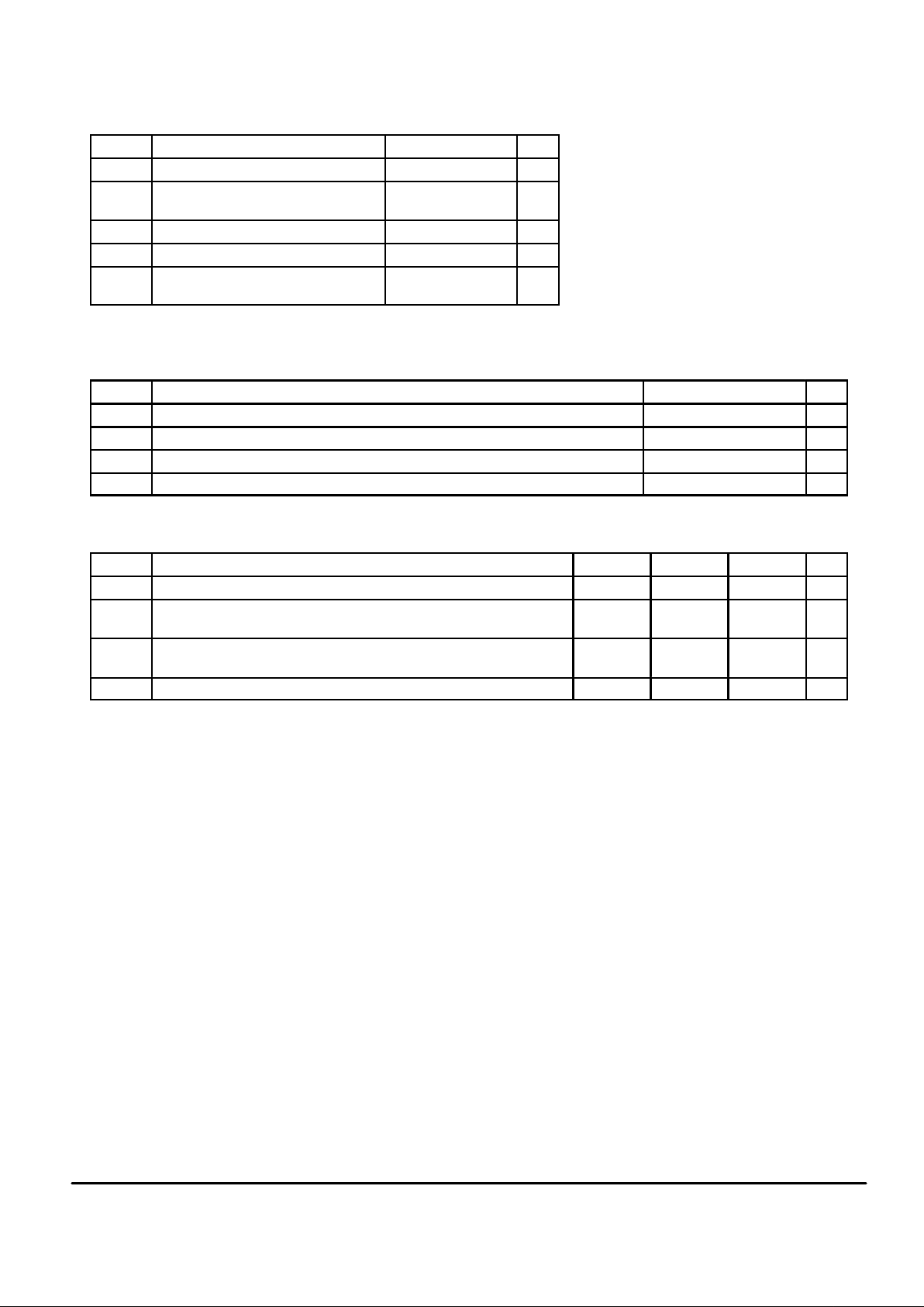
MAXIMUM RATINGS* (Voltages Referenced to V
SS
)
Symbol
Parameter Value Unit
V
DD
DC Supply Voltage 6.0 V
V
in
DC Input Voltage, Any Digital Input VSS – 0.5 to
VDD + 0.5
V
I
in
DC Input Current, per Pin ±10 mA
T
stg
Storage Temperature – 55 to 150 °C
T
L
Lead Temperature, 1 mm from Case for
10 Seconds
260 °C
*Maximum Ratings are those values beyond which damage to the device may occur. Func-
tional operation should be restricted to the Operation Ranges below.
OPERATION RANGES (Applicable to Guaranteed Limits)
Symbol
Parameter Value Unit
V
DD
DC Supply Voltage, Referenced to V
SS
4.5 to 5.5 V
Vin, V
out
Digital Input/Output Voltage VSS – 0.5 to VDD + 0.5 V
I
D
Input Pin Current Drain 1 µA
T
A
Operating Temperature – 40 to + 85 °C
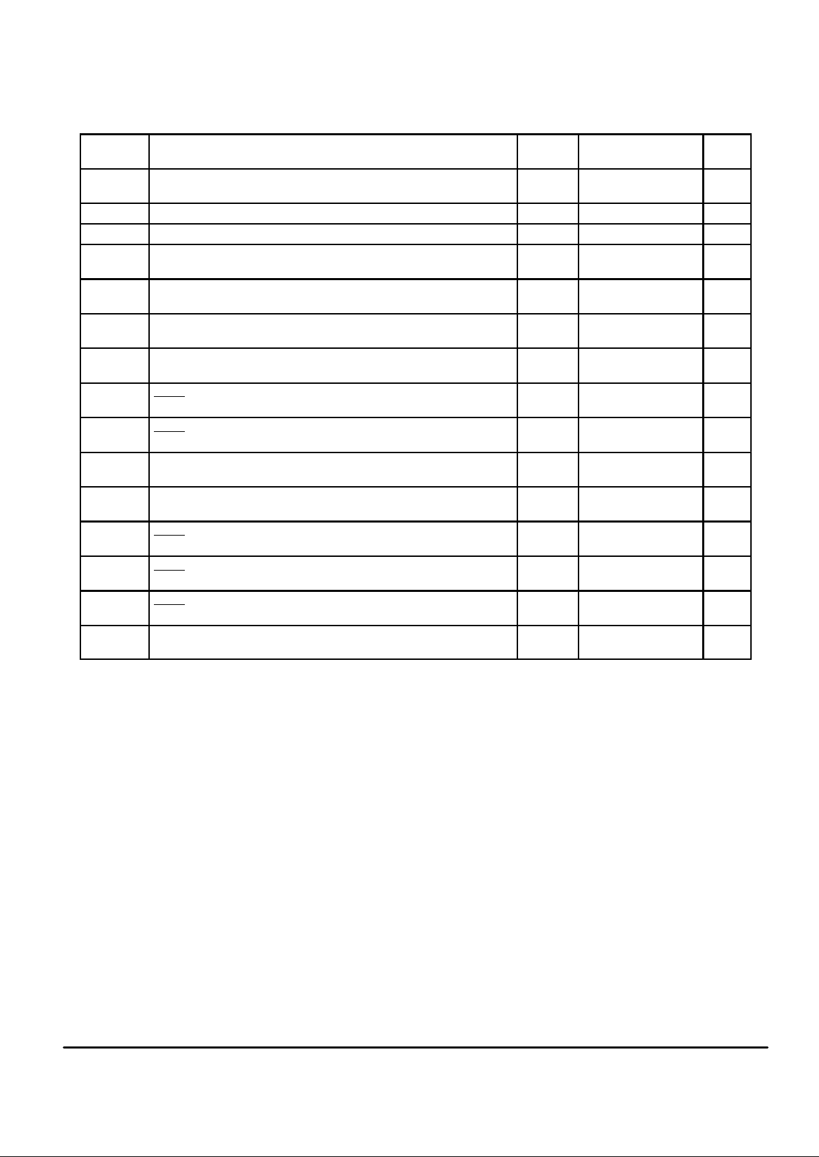
DC ELECTRICAL CHARACTERISTICS
(Voltages Referenced to VSS, Full T emperature and Voltage Ranges per Operation Ranges table, unless otherwise indicated)
Symbol
Parameter Min Typ Max Unit
I
dd
Power Supply Current — — 10 mA
V
IL
V
IH
Input Voltage Low Level Input
High Level Input—VDD x 0.7
—
—
VDD x 0.3—V
V
OL
V
OH
Output Voltage Low Level Output (Load = 0.4 mA)
High Level Output (Load = 0.4 mA)—VDD – 0.3
—
—
0.3
—
V
I
lkg
Input Leakage Current — — ± 10 µA
This device contains protection circuitry to
guard against damage due to high static voltages or electric fields. However, precautions
must be taken to avoid applications of any voltage higher than maximum rated voltages to
this high–impedance circuit. For proper operation, Vin and V
out
should be constrained to the
range VSS ≤ (Vin or V
out
) ≤ VDD.
Unused inputs must always be tied to an
appropriate logic voltage level (e.g., either V
SS
or VDD). Unused outputs must be left open.

MC145074
3
MOTOROLA
AC ELECTRICAL CHARACTERISTICS
(Full Temperature and Voltage Ranges per Operation Ranges Table at 50 pf Loads on Outputs)
Symbol
Parameter Figure
Guaranteed
Limit
Unit
Operating Frequency Xin(DIV2 = 0)
(DIV2 = 1)
18.5
37.0
MHz
Bit Clock Frequency 18.5 MHz
tr, t
f
Maximum Rise and Fall Times (BCKL, WCLK) 2, 5 6 ns
t
PLH
t
TLH
X
out
L–H Propagation Delay
X
out
Rise Time
2 30
15
ns
t
PHL
t
THL
X
out
H–L Propagation Delay
X
out
Fall Time
2 30
15
ns
t
PLH
t
TLH
DOL, DOR L–H Propagation Delays
DOL, DOR Rise Time
3 15
5
ns
t
PHL
t
THL
DOL, DOR H–L Propagation Delays
DOL, DOR Fall Time
3 15
5
ns
t
PLH
t
TLH
WCLK Output L–H Propagation Delay
WCLK
Output Rise Time
4 15
5
ns
t
PHL
t
THL
WCLK Output H–L Propagation Delay
WCLK
Output Fall Time
4 15
5
ns
t
su
t
h
DIR Master Program Mode Minimum Setup Time
DIR Master Program Mode Minimum Hold Time
5 5
5
ns
t
su
t
h
DIR, DIL Minimum Setup Time
DIR, DIL Minimum Hold Time
5 5
5
ns
t
su
t
h
WCLK Minimum Setup Time to BCLK (not DMODE = WDLY = 1)
WCLK
Minimum Hold Time to BCLK (not DMODE = WDLY = 1)
6 5
5
ns
t
su
t
h
WCLK Minimum Setup Time to Xin (not DMODE = WDLY = 1)
WCLK
Minimum Hold Time to Xin (not DMODE = WDLY = 1)
6 5
5
ns
t
su
t
h
WCLK Minimum Setup Time to BCLK (DMODE = WDLY = 1)
WCLK
Minimum Hold Time to BCLK (DMODE = WDLY = 1)
7 5
5
ns
t
LAG
t
LEAD
BCLK to Xin (1st Edge Only) Lag Time (DMODE = WDLY = 1)
BCLK to Xin (1st Edge Only) Lead Time (DMODE = WDLY = 1)
7 5
5
ns

MC145074
MOTOROLA
4
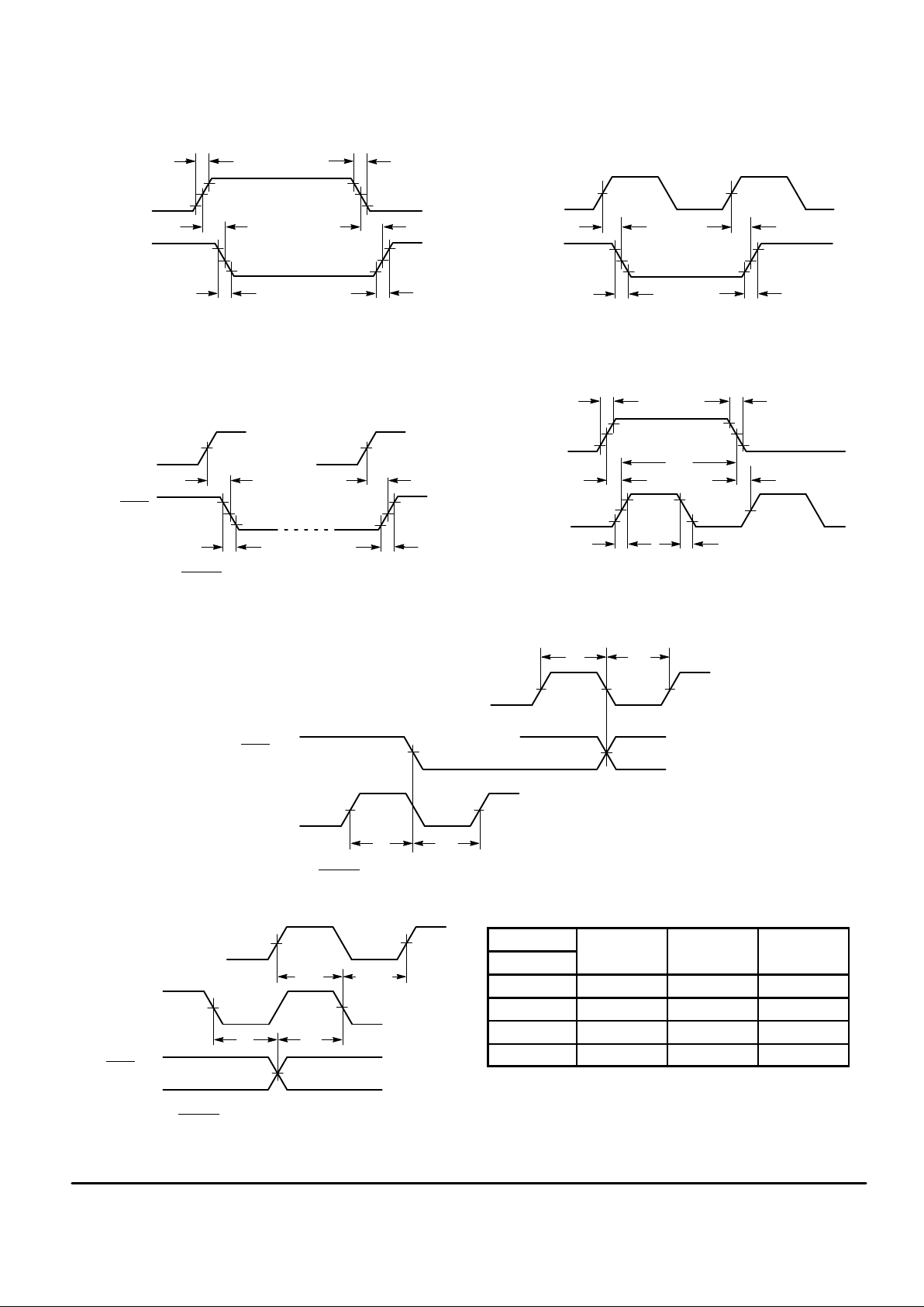
SWITCHING W AVEFORMS
10%
X
in
90%
50%
t
r
t
PHL
90%
50%
10%
t
f
10%
90%
50%
90%
50%
10%
t
PLH
t
THL
t
TLH
X
out
Figure 1. X
out
Propagation Delay Timing
50%
10%
90%
50%
90%
50%
10%
t
THL
t
TLH
50%X
in
DOL/DOR
t
PHL
t
PLH
Figure 2. DOL/DOR Propagation Delay Timing
X
in
50%
t
PHL
10%
90%
50%
90%
50%
10%
t
PLH
t
THL
t
TLH
WCLK
50%
Figure 3. WCLK Out Propagation Delay Timing
(Master Mode)
10%
90%
BCLK
DIL/DIR/DILR
t
f
50%
90%
50%
t
r
10%
t
h
t
r
t
f
t
su
t
su
Figure 4. DIL/DIR/DILR Setup and Hold Timing
BCLK
WCLK
50%
50%
50%
t
h
t
su
t
su
t
h
X
in
Figure 5. WCLK Timing (All Modes Except DMODE = 1, WDLY = 1)
X
in
WCLK
50%
50%
50%
t
LAG
t
LEAD
t
su
t
h
BCLK
Figure 6. WCLK Timing (DMODE = 1, WDLY = 1)
Bits 16 18 20
OSR
S/(N+D) dB S/(N+D) dB S/(N+D) dB
128x 90 90 90
192x 94 98 99
256x 95 103 105
384x 96 107 113
NOTE: Values are for 0 dB input signal, 0 – 20 kHz BW , and 44.1 kHz
1x fs Sampling Rate.
Figure 7. Digital S/(N+D) Performance Levels

MC145074
5
MOTOROLA
PIN DESCRIPTIONS
V
DD
Positive Device Supply (Pin 1)
VDD is the positive supply, nominally + 5 volts.
STBY
Active–Low Standby Input (Pin 2)
A low level on the STBY pin will force the device into a
standby state. If the device is being operated in the master
mode (MSTR = 1), the WCLK
internal divider can be
programmed using the DIR/DILR, and BCLK pins while
the STBY
pin is active. When the device is in standby, the
DOL and DOR pins will output a 50% duty cycle data stream
that will generate a 1/2 scale analog output, when averaged
through the output filter.
DIL/WDLY
Left Channel Data/Word Clock Delay Input (Pin 3)
When the DMODE pin is low, this pin is the left channel
(MSB first) 2’s complement serial data input. When the
DMODE pin is high, this pin controls the WCLK
delay. A high
level on this pin will delay the WCLK an additional clock cycle
internal to the device.
DIR/DILR
Right Channel Data/Multiplexed Left – Right Data Input
(Pin 4)
When the DMODE pin is low, this pin is the right channel
(MSB first) 2’s complement serial data input. When the
DMODE pin is high, this pin is the multiplexed left then right
channel data input. If the part is being operated in the master
mode (MSTR = 1), the WCLK
internal divider can be programmed by clocking control word data onto this pin with the
BCLK pin while the device is in the standby mode (STBY
= 0).
BCLK
Bit Clock Input (Pin 5)
The BCLK pin provides the serial bit shift clock for the left
and right channel data in all modes of operation. A rising
edge on the BCLK pin shifts serial data into the device.
WCLK
Word Clock Output/Input (Pin 6)
The WCLK pin is used to latch the shifted serial data word
into the device. The MC145074 can accept an external word
clock when in the slave mode, or can use an internally
generated word clock when operating in the master mode.
When DMODE is low, left and right channel data is latched
into the device on the falling edge of WCLK
. When DMODE
is high, left channel data is latched on the rising edge of
WCLK
and right channel data is latched on the falling edge of
WCLK
with both channel inputs being input to the modulator
on the next rising edge of WCLK. The internal divide ratio
used to generate WCLK
, as well as the rising or falling edge
latching of the input data can be programmed using the DIR/
DILR and BCLK pins while the device is in the standby mode.
MSTR
Active–High Master Mode Select Input (Pin 7)
A high level on the MSTR pin will select the master mode
of operation. In the master mode, the MC145074 will
generate and output a word clock signal on the WCLK
pin. A
low level on the MSTR pin will place the MC145074 in the
slave mode, and the WCLK
signal must be provided by an
external source. The default master mode divide rate is
MODCLK/64.
V
SS
Device Ground (Pin 8)
VSS is normally connected to ground.
DOR
Right Channel Data Output (Pin 9)
DOR is the right channel modulator data output.
DIV2
Master Clock Divide Control Input (Pin 10)
DIV2 is the Xin divide by two control pin. When cleared, the
Xin pin directly provides the modulator clock (MODCLK), and
the data output bit streams are not chopped. When this pin is
set, the Xin clock is divided by two to provide the modulator
clock and the output data bit stream is chopped at the Xin frequency using an alternating 1,0 chop. The chop is used to
reduce even order distortion for a stand–alone application
without the MC145076. The reconstructed output signal will
drop 6dB due to the chopping.
X
out
Master Clock Output (Pin 11)
X
out
is the inverted output signal of Xin and may be used
for a buffered clock output or for a crystal oscillator.
X
in
Master Clock Input (Pin 12)
Xin is the input clock pin for the MC145074, and may be
used with X
out
as the inverter for a crystal oscillator.
DMODE
Data Mode Input (Pin 13)
A low level on the DMODE pin will select the dual data pin
mode of operation. In this mode, the serial input data is
entered on the DIR and DIL pins. A high level on the DMODE
pin selects the multiplexed mode of operation. In this mode,
the left and right channel serial input data must be multiplexed on the DIR/DILR pin.
RES0 and RES1
Input Data Resolution Pins (Pins 14, 15)
The RES0 and RES1 pins select the length of the serial
data word input to the MC145074. The serial input data can
be 16, 18, or 20–bits in length with the most significant bits
clocked in first. Figure 9 lists the serial interface formats.
DOL
Left Channel Data Output (Pin 16)
DOL is the left channel modulator data output.
 Loading...