Motorola MC145073DW Datasheet
MOTOROLA
MC145073
1
Product Preview
CMOS
The MC145073 is a dual–channel, 16–bit A/D converter intended for use in
digital audio systems such as multimedia, DCC, DAT, and professional audio
applications. It uses a sigma–delta architecture consisting of a second–order
analog modulator and two stages of digital filtering for each channel. The
analog modulator samples the input signal at 128 times the output data rate,
performs a single–bit quantization, and shapes the quantization noise towards
higher frequencies. Subsequent on–chip digital filters reject most of the shaped
quantization noise and lower the data rate.
Sixteen unique user–selectable interfacing modes make the MC145073
compatible with a multitude of application interfacing requirements. A single 5 V
supply and a power–down mode reduce power supply requirements, making
the part attractive for portable applications.
• Single Supply, Operating Voltage Range: 4.5 to 5.5 V
• 128x OSR Sigma–Delta Modulator
• 82 dB Typical S/(N+D)
• Analog Inputs Can Be Driven as Either Differential or Single–Ended
• Clock Input May Be 128x, 256x, or 384x the Output Data Rate
• Out–of–Range Input Signals Internally Limited
• On–Chip Digital Filters:
5th Order Decimate–by–32 Comb Filter
121 Tap Decimate–by–4 FIR Filter
• User–Selectable Digital Filter Transition Bands
• Versatile Serial Digital Output Interface:
Configurable as Master or Slave
Data Can Be Either Left– or Right–Justified
Interfaces to DSP56000/1 and TMS320 DSPs
I2S or Japanese Interface Compatibility
CS5326 Compatible Interface Mode
Multiplexing of Two MC145073s Accommodated
• Power–Down Mode Consumption: 2.0 mW
• Operating Temperature Range: – 40 to 85°C
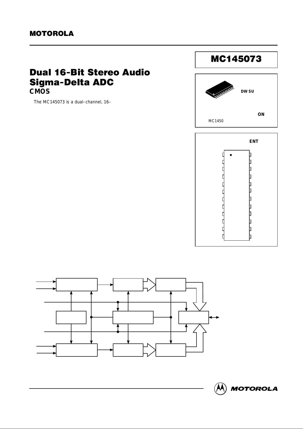
MODULA TOR
A
IN(+L)
A
IN(–L)
COMB FILTER
A
IN(+R)
A
IN(–R)
MODULA TOR
COMB FILTER
VOLTAGE
REFERENCE
CLK
MODES
IN
CLK DIVIDERS/DRIVER
AND CONTROL LOGIC
FIR FILTER
FIR FILTER
SERIAL
INTERFACE
DIGITAL
INTERFACE
This document contains information on a product under development. Motorola reserves the right to change or discontinue this product without notice.
TMS320 is a trademark of Texas Instruments.
Order this document
by MC145073/D
SEMICONDUCTOR TECHNICAL DATA
PIN ASSIGNMENT
DW SUFFIX
SOG PACKAGE
CASE 751E
ORDERING INFORMATION
MC145073DW SOG Package
CSEL1
FSEL
V
AG
V
DD(D)
V
DD(A)
A
IN(+L)
A
IN(–L)
REF
VSS(A)
SUB
V
SS(D)
FTP
FTP
SYNC
SCLK
A
IN(+R)
A
IN(–R)
CSEL0
I
SYNC
I
SLAV
I
JUST
I
DOE
CLK
SDO
5
4
3
2
1
10
9
8
7
6
14
15
16
17
18
19
20
13
11
12
21
22
23
24
1
24
Motorola, Inc. 1997
REV 1
5/97
MC145073
MOTOROLA
2
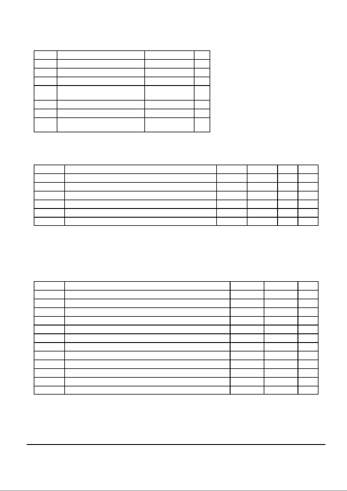
MAXIMUM RATINGS* (Voltages referenced to V
SS
, unless otherwise stated)
Symbol
Parameter Value Unit
V
DD(A)
Analog Supply Voltage 6.0 V
V
DD(D)
Digital Supply Voltage 6.0 V
I
in
DC Input Current, per Pin ± 20 mA
V
in(A)
Analog Input Voltage V
SS(A)
– 0.3 to
V
DD(A)
+ 0.3
V
V
in(D)
Digital Inputs – 0.3 to V
DD(D)
+ 0.3 V
T
stg
Storage Temperature – 65 to 150 °C
T
l
Lead Temperature 1 mm From Case for
10 Seconds
260 °C
*Maximum Ratings are those values beyond which damage to the device may occur.
Functional operation should be restricted to the Operation Ranges, Analog Specifications,
AC Electrical Characteristics, and DC Electrical Characteristics tables.
OPERATION RANGES
Symbol Parameter Min Max Unit Note
V
DD(A)
Analog Supply Voltage 4.5 5.5 V
V
DD(D)
Digital Supply Voltage 4.5 5.5 V
V
in(A)
Analog Input Voltage (A
IN(+L)
, A
IN(–L)
, A
IN(+R)
, A
IN(–R)
) — 1.9 V p–p 1
f
CLK
CLK Frequency 3.072 18.432 MHz 2
C
LOAD
Capacitive Load on Any Output 0 50 pF
T
a
Ambient Operating Temperature – 40 85 °C
NOTES:
1. Differential inputs greater than 3.8 V p–p will overload the modulators. These voltages are subject to the gain error tolerance specifications
in the Analog Specifications table.
2. The internal clock frequency or input sampling frequency is governed by the divide mode and output data rate. The divide mode can be either
1, 2, or 3. The output data rate ranges from 24 kHz to 48 kHz. The minimum clock frequency of 3.072 MHz is for a 24 kHz output rate in the
clock divide by 1 mode. The maximum clock frequency of 18.432 MHz is for a 48 kHz output rate in the clock divide by 3 mode.
DC ELECTRICAL SPECIFICATIONS
(Voltages referenced to V
SS(D)
; Full T emperature and Voltage Ranges per Operation Ranges Table, unless otherwise indicated.)
Symbol
Parameter Min Max Unit
V
IH
Minimum High–Level Digital Input Voltage 0.7 x V
DD(D)
V
V
IL
Maximum Low–Level Digital Input Voltage 0.3 x V
DD(D)
V
I
IN
Maximum Input Leakage Current 10 µA
V
OH
Minimum High–Level Digital Output Voltage (IOH = – 20 µA) 4.4 V
V
OL
Maximum Low–Level Digital Output Voltage (IOL = 20 µA) 0.1 V
I
DDu(D)
Maximum Digital Power Supply Current, Operating 45 mA
I
DDd(D)
Maximum Digital Power Supply Current, Power–Down 250 µA
I
DDu(A)
Maximum Analog Power Supply Current, Operating 10 mA
I
DDd(A)
Maximum Analog Power Supply Current, Power–Down 150 µA
P
O
Power Consumption, Operating 250 mW
P
pd
Power Consumption, Power–Down 2.0 mW
Cin Maximum Input Capacitance 20 pF
This device contains protection circuitry to
guard against damage due to high static voltages or electric fields. However, precautions
must be taken to avoid applications of any voltage higher than maximum rated voltages to this
high–impedance circuit.
MOTOROLA
MC145073
3
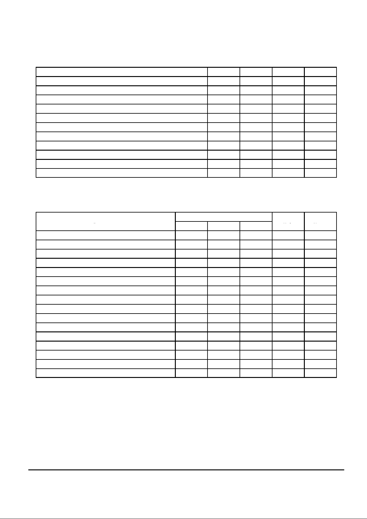
ANALOG SPECIFICATIONS
(Full T emperature, CLK = 6.144 MHz in div1, V
DD(A)
= V
DD(D)
= 5.0 V , 1007.8 Hz Full–Scale Input Sinewave, 1.4 V p–p @ A
IN(L)
and A
IN(R)
,
Common Mode Input Voltage = 2.5 V. Measured bandwidth is 23 Hz to 24 kHz, inputs driven differentially per Figure 1.)
Parameter
Min Typ Max Unit
Resolution Bits 16 Bits
S/(N+D) 76 82 dB
Dynamic Range 85 dB
Total Harmonic Distortion (Vin = ± F.S.) .003 %
Gain Error ± 5 %
Gain Drift 50 ppm/°C
Channel to Channel Isolation 90 dB
PSRR (V
DD(A)
) 60 dB
PSRR (V
DD(D)
) 100 dB
Input Impedance 40 kΩ
Warm–Up Time (for Reference and Bias Circuits) 1 ms
DIGITAL FILTER CHARACTERIZATION
(Over full operating ranges per Operating Ranges table. Stated values are for input/output relationships from input of comb filter to output of
FIR filter.)
Output Data Rate
Parameter
32 kHz 44.1 kHz 48 kHz
Unit Notes
FSEL = low
FIR Filter Passband 0 to 13.3 0 to 18.3 0 to 20 kHz
Maximum Passband Ripple ± 0.1 ± 0.1 ± 0.1 dB
FIR Filter Transition Band 13.3 to 17 18.3 to 23.5 20 to 25.8 kHz
FIR Filter Rejection (Min) – 84 – 84 – 84 dB
Maximum Alias Level (Figure 3) – 86 – 86 – 86 dB 1, 2
Group Delay 33 33 33 Out CLKS 3
Setting Time 49 49 49 Out CLKS 3
FSEL = high
FIR Filter Passband 0 to 14.5 0 to 20 0 to 21.7 kHz
Maximum Passband Ripple ± 0.1 ± 0.1 ± 0.1 dB
FIR Filter Transition Band 14.5 to 18.2 20 to 25.0 21.7 to 27.3 kHz
FIR Filter Rejection (Min) – 84 – 84 – 84 dB
Maximum Alias Level (Figure 3) – 86 – 86 – 86 dB 1, 2
Group Delay 33 33 33 Out CLKS 3
Setting Time 49 49 49 Out CLKS 3
NOTES:
1. There is no rejection of input signals that are multiples of the sampling frequency (nxCLKI ± Filter Bandwidth, where n = 0, 1, 2, ...).
2. The maximum alias level spec does not apply to input signals in the range of 24 to 25.8 kHz in the 48 kHz output mode, 22.05 to 23.675 kHz
in the 44.1 kHz output mode, or 16 to 17.2 kHz in the 32 kHz output mode.
3. One Out CLK (output clock) is equal in length to 128 internal CLKs or one SYNC clock period.
MC145073
MOTOROLA
4
+
–
V
DD(A)
A
IN(R)
R
IN
1 k
Ω
2
3
6
5
U2A
U2B
A
OUT(–R)
A
OUT(+R)
+
–
1
7
1 k
Ω
1 k
Ω
V
DD(A)
+
–
A
IN(L)
R
IN
1 k
Ω
2
3
6
5
U1A
U1B
A
OUT(–L)
A
OUT(+L)
+
–
1
7
V
DD(A)
1 k
Ω
1 k
Ω
V
DD(A)
V
DD(A)
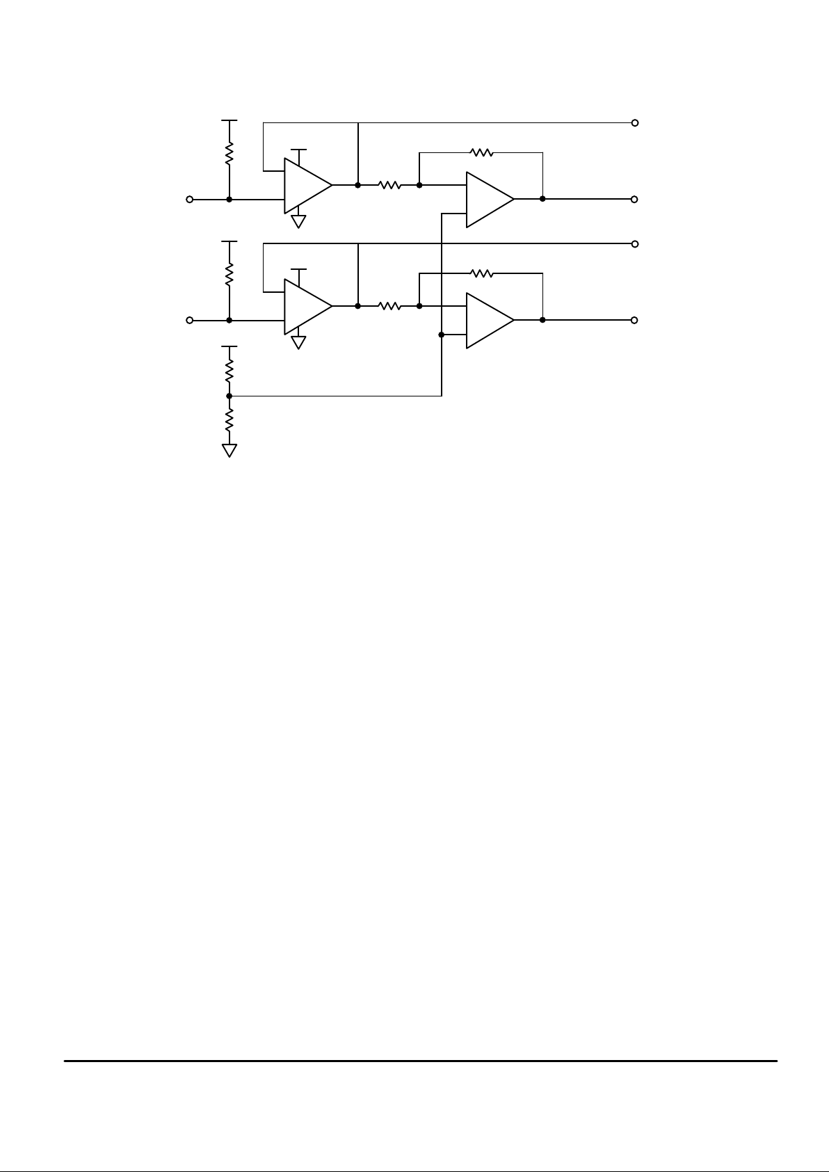
Figure 1. Input Buffer–Driver
NOTES:
1. Analog signals A
IN(L)
and A
IN(R)
are floating drivers. R
OUT
of source is to be equal to RIN of resistors.
2. U1, U2 — MC33077.
MOTOROLA
MC145073
5
*A
IN(–R)
*A
IN(+R)
*A
IN(–L)
*A
IN(+L)
1000 pF
0.1
µ
F
4
V
DD(A)
5
V
SS(A)
8
V
DD(D)
7
V
SS(D)
1AIN
(+L)
2AIN
(–L)
24 AIN
(+R)
23 AIN
(–R)
22 V
AG
3 REF
SCLK 12
SYNC 11
SDO 13
FSEL 19
CSEL0 21
CSEL1 20
CLK 14
AUDIO
DATA
PROCESSOR
CONTROLLER
MC74HCU04
11.2896 MHz
FOR 44.1 kHZ
USER SELECTABLE
DIGITAL STATES
SUB6I
DOE
15
I
SLAV
17
I
SYNC
18
I
JUST
16
FTP9FTP
10
1000 pF
1000 pF
1000 pF
1 µF0.1 µF1 µF
820 k
Ω
22 pF
33
33
33
33
0.1
µ
F
47 µF
V
DD(A)
V
DD(D)
1 µF
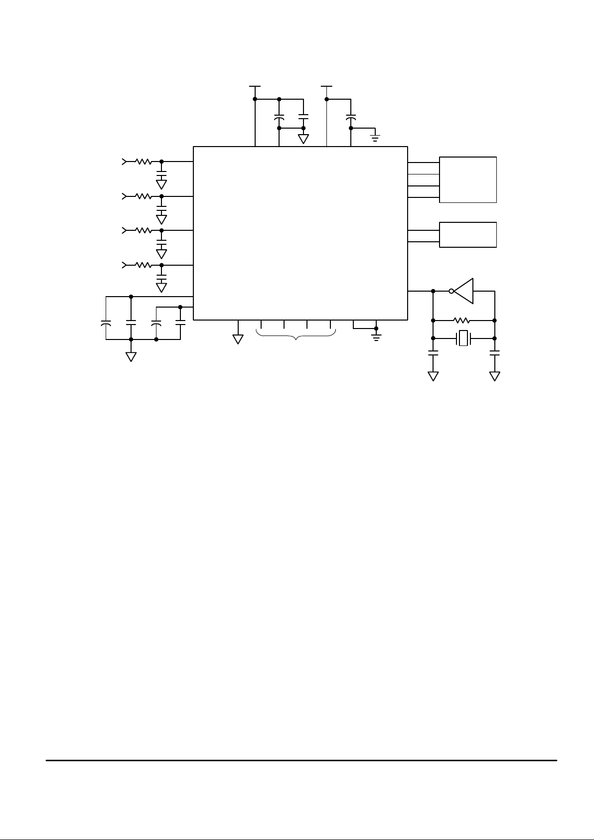
* For best performance A
IN(+L)
, A
IN(–L)
and A
IN(+R)
, A
IN(–R)
should be differentially driven. A
IN(+L)
or A
IN(+R)
(and
A
IN(–L)
or A
IN(–R)
) can be grounded for single ended configuration. Circuit in Figure 1 depicts input buffer circuit.
22 pF
Figure 2. MC145073 A/D Application Circuit
 Loading...