

SEMICONDUCTOR TECHNICAL DATA
Order this document
by MC145053/D
CMOS
This ratiometric 10-bit ADC has a serial interface port to provide communi-
cation with MCUs and MPUs.
Either a 10- or 16-bit format can be used
16-bit format can be one continuous 16-bit stream or two intermittent 8-bit
streams. The converter operates from a single power supply with no external
trimming required. Reference voltages down to 4.0 V are accommodated.
The MC145053 has an internal clock oscillator to operate the dynamic A/D
conversion sequence and an end-of-conversion (EOC) output.
• 5 Analog Input Channels with Internal Sample-and-Hold
• Operating Temperature Range: – 40 to 125° C
• Successive Approximation Conversion Time: 44 µs Maximum
• Maximum Sample Rate: 20.4 ks/s
• Analog Input Range with 5-Volt Supply: 0 to 5 V
• Monotonic with No Missing Codes
• Direct Interface to Motorola SPI and National MICROWIRE Serial Data
Ports
• Digital Inputs/Outputs are TTL, NMOS, and CMOS Compatible
• Low Power Consumption: 14 mW
• Chip Complexity: 1630 Elements (FETs, Capacitors, etc.)
• See Application Note AN1062 for Operation with QSPI
BLOCK DIAGRAM
V
ref
98
MUX OUT
10-BIT RC DAC
WITH SAMPLE AND HOLD
. The
V
AG
P SUFFIX
PLASTIC
CASE 646
D SUFFIX
SOG
CASE 751A
ORDERING INFORMATION
MC145053P Plastic DIP
MC145053D SOG Package
PIN ASSIGNMENT
EOC
AN0
AN1
AN2
AN3
AN4
V
SS
1
2
3
4
6
7
14
13
12
11
105
V
DD
SCLK
D
in
D
out
CS
9
V
ref
V
8
AG
2
AN0
3
AN1
AN2
AN3
AN4
INTERNAL
TEST
VOLTAGES
MICROWIRE is a trademark of National Semiconductor Corp.
REV 2
1/99
MOTOROLA WIRELESS SEMICONDUCTOR
Motorola, Inc. 1998
SOLUTIONS DEVICE DA TA
AN5
AN6
AN7
D
in
D
out
CS
SCLK
EOC
4
5
6
12
11
10
13
ANALOG
MUX
1
MUX ADDRESS
REGISTER
DIGITAL CONTROL
LOGIC
SUCCESSIVE APPROXIMA TION
REGISTER
DATA REGISTER
PIN 14 = V
DD
PIN 7 = V
SS
AUTO-ZEROED
COMPARATOR
MC145053
1
MAXIMUM RATINGS*
Symbol Parameter Value Unit
V
V
V
V
I
IDD, ISSDC Supply Current, VDD and VSS Pins ± 50 mA
T
*Maximum Ratings are those values beyond which damage to the device may occur. Func-
tional operation should be restricted to the Operation Ranges below..
DC Supply Voltage (Referenced to VSS) – 0.5 to + 6.0 V
DD
DC Reference Voltage VAG to VDD + 0.1 V
ref
Analog Ground VSS – 0.1 to V
AG
V
DC Input Voltage, Any Analog or Digital
in
Input
DC Output Voltage VSS – 0.5 to
out
I
DC Input Current, per Pin ± 20 mA
in
DC Output Current, per Pin ± 25 mA
out
Storage Temperature – 65 to 150 °C
stg
T
Lead Temperature, 1 mm from Case for
L
10 Seconds
VSS – 0.5 to
VDD + 0.5
VDD + 0.5
260 °C
ref
V
V
V
OPERATION RANGES (Applicable to Guaranteed Limits)
Symbol
V
V
V
Vin, V
NOTE: Analog input voltages greater than V
DC Supply Voltage, Referenced to V
DD
DC Reference Voltage VAG + 4.0 to VDD + 0.1 V
ref
Analog Ground VSS – 0.1 to V
AG
V
Analog Input Voltage (See Note) VAG to V
AI
Digital Input Voltage, Output Voltage VSS to V
out
T
Ambient Operating Temperature – 40 to 125 °C
A
descriptions.
Parameter Value Unit
SS
convert to full scale. Input voltages less than VAG convert to zero. See V
ref
This device contains protection circuitry to
guard against damage due to high static
voltages or electric fields. However, precautions must be taken to avoid applications
of any voltage higher than maximum rated
voltages to this high-impedance circuit. For
proper operation, Vin and V
constrained to the range VSS ≤ (Vin or V
VDD.
Unused inputs must always be tied to an
appropriate logic voltage level (e.g., either
VSS or VDD). Unused outputs must be left
open.
4.5 to 5.5 V
should be
out
– 4.0 V
ref
ref
DD
and VAG pin
ref
out
) ≤
V
V
DC ELECTRICAL CHARACTERISTICS
(Voltages Referenced to VSS, Full T emperature and Voltage Ranges per Operation Ranges T able, unless otherwise indicated)
Guaranteed
Symbol
V
IH
V
IL
V
OH
V
OL
I
in
I
OZ
I
DD
I
ref
I
Al
Parameter Test Condition
Minimum High-Level Input Voltage
(Din, SCLK, CS
Maximum Low-Level Input Voltage
(Din, SCLK, CS
Minimum High-Level Output Voltage
(D
, EOC)
out
Minimum Low-Level Output Voltage
(D
, EOC)
out
Maximum Input Leakage Current
(Din, SCLK, CS
Maximum Three-State Leakage Current (D
Maximum Power Supply Current Vin = VSS or VDD, All Outputs Open 2.5 mA
Maximum Static Analog Reference Current (V
Maximum Analog Mux Input Leakage Current between all
deselected inputs and any selected input (AN0 – AN4)
)
)
I
= – 1.6 mA
out
I
= – 20 µA
out
I
= + 1.6 mA
out
I
= + 20 µA
out
)
) V
out
) V
ref
Vin = VSS or V
= VSS or V
out
= VDD, VAG = V
ref
VAl = VSS to V
DD
DD
SS
DD
Limit
VDD – 0.1
Unit
2.0 V
0.8 V
2.4
0.4
0.1
± 2.5 µA
± 10 µA
100 µA
± 1 µA
V
V
MC145053
2
MOTOROLA WIRELESS SEMICONDUCTOR
SOLUTIONS DEVICE DA TA
A/D CONVERTER ELECTRICAL CHARACTERISTICS
(Full Temperature and Voltage Ranges per Operation Ranges Table)
Guaranteed
Characteristic
Resolution Number of bits resolved by the A/D converter 10 Bits
Maximum Nonlinearity Maximum difference between an ideal and an actual ADC transfer function ± 1 LSB
Maximum Zero Error Difference between the maximum input voltage of an ideal and an actual
ADC for zero output code
Maximum Full-Scale Error Difference between the minimum input voltage of an ideal and an actual
ADC for full-scale output code
Maximum Total Unadjusted Error Maximum sum of nonlinearity, zero error, and full-scale error ± 1 LSB
Maximum Quantization Error Uncertainty due to converter resolution ± 1/2 LSB
Absolute Accuracy Difference between the actual input voltage and the full-scale weighted
equivalent of the binary output code, all error sources included
Maximum Conversion Time Total time to perform a single analog-to-digital conversion 44 µs
Data Transfer Time Total time to transfer digital serial data into and out of the device 10 to 16 SCLK
Sample Acquisition Time Analog input acquisition time window 6 SCLK
Minimum Total Cycle Time Total time to transfer serial data, sample the analog input, and perform the
conversion; SCLK = 2.1 MHz
Maximum Sample Rate Rate at which analog inputs may be sampled; SCLK = 2.1 MHz 20.4 ks/s
Definition and Test Conditions
Limit
± 1 LSB
± 1 LSB
± 1-1/2 LSB
49 µs
Unit
cycles
cycles
MOTOROLA WIRELESS SEMICONDUCTOR
SOLUTIONS DEVICE DA TA
MC145053
3
AC ELECTRICAL CHARACTERISTICS
(Full Temperature and Voltage Ranges per Operation Ranges Table)
Figure
1 f Clock Frequency, SCLK (10-bit xfer) Min
1 t
1 t
1, 7 t
1, 7 t
2, 7 t
2, 7 t
3 t
3 t
4, 7, 8 t
5 t
— t
— t
5 t
6, 8 t
1 tr, t
1, 4, 6 – 8 t
— C
— C
NOTES:
1. After the 10th SCLK falling edge (≤ 2 V), at least 1 SCLK rising edge (≥ 2 V) must occur within 18.5 µs.
2. A CS
Symbol Parameter
Note: Refer to twH, twL below (10- to 16-bit xfer) Max)
wH
wL
, t
PLH
h
, t
PLZ
, t
PZL
su
h
d
su
CSd
CAs
h
PHL
, t
TLH
out
edge may be received immediately after an active transition on the EOC pin.
Minimum Clock High Time, SCLK 190 ns
Minimum Clock Low Time, SCLK 190 ns
Maximum Propagation Delay, SCLK to D
PHL
Minimum Hold Time, SCLK to D
Maximum Propagation Delay, CS to D
PHZ
Maximum Propagation Delay, CS to D
PZH
Minimum Setup Time, Din to SCLK 100 ns
Minimum Hold Time, SCLK to D
Maximum Delay Time, EOC to D
Minimum Setup Time, CS to SCLK 2.425 µs
Minimum Time Required Between 10th SCLK Falling Edge (≤ 0.8 V) and
CS
to Allow a Conversion
Maximum Delay Between 10th SCLK Falling Edge (≤ 2 V) and CS to
Abort a Conversion
Minimum Hold Time, Last SCLK to CS 0 ns
Maximum Propagation Delay, 10th SCLK to EOC 2.35 µs
Maximum Input Rise and Fall Times SCLK
f
Maximum Output Transition Time, Any Output 300 ns
THL
Maximum Input Capacitance AN0 – AN4
in
Maximum Three-State Output Capacitance D
out
in
out
High-Z 150 ns
out
Driven 2.3 µs
out
(MSB) 100 ns
out
(11- to 16-bit xfer) Min
Din, CS
SCLK, CS
, D
out
Guaranteed
Limit
0
Note 1
2.1
125 ns
10 ns
0 ns
Note 2
9 µs
1
10
55
in
15
15 pF
Unit
MHz
ms
µs
pF
MC145053
4
MOTOROLA WIRELESS SEMICONDUCTOR
SOLUTIONS DEVICE DA TA
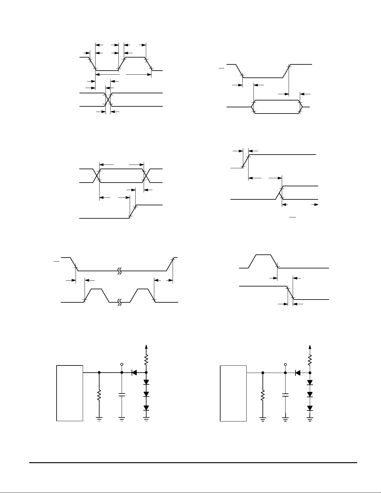
SWITCHING WAVEFORMS
SCLK
D
out
D
SCLK
in
t
f
2.0 V
t
h
t
wL
0.8 V
2.4 V
0.4 V
Figure 1.
VALID
2.0 V
0.8 V
t
su
1/f
t
PLH
t
TLH
, t
t
wH
PHL
, t
t
r
THL
0.8 V
2.0 V
PZL
2.0 V
90%
10%
t
PHZ
, t
PLZ
CS
D
out
0.8 V
2.4 V
0.4 V
t
PZH
, t
Figure 2.
t
TLH
EOC
0.4 V
t
h
D
out
NOTE: D
2.4 V
t
d
2.4 V
0.4 V
VALID MSB
is driven only when CS is active (low).
out
CS
SCLK
DEVICE
UNDER
TEST
0.8 V
D
Figure 3.
t
su
FIRST
CLOCK
Figure 5.
out
12 k 100 pF
TEST
POINT
LAST
CLOCK
V
DD
0.8 V0.8 V
2.18 k
2.0 V
t
h
SCLK
EOC
DEVICE
UNDER
TEST
10TH
CLOCK
EOC
Figure 4.
0.8 V
2.4 V
t
THL
Figure 6.
TEST
POINT
12 k 50 pF
t
0.4 V
PHL
V
DD
2.18 k
Figure 7. T est Circuit
MOTOROLA WIRELESS SEMICONDUCTOR
SOLUTIONS DEVICE DA TA
Figure 8. T est Circuit
MC145053
5
 Loading...