

Motorola MC14504BD, MC14504BCL, MC14504BCP Datasheet
MOTOROLA CMOS LOGIC DATAMC14504B
332
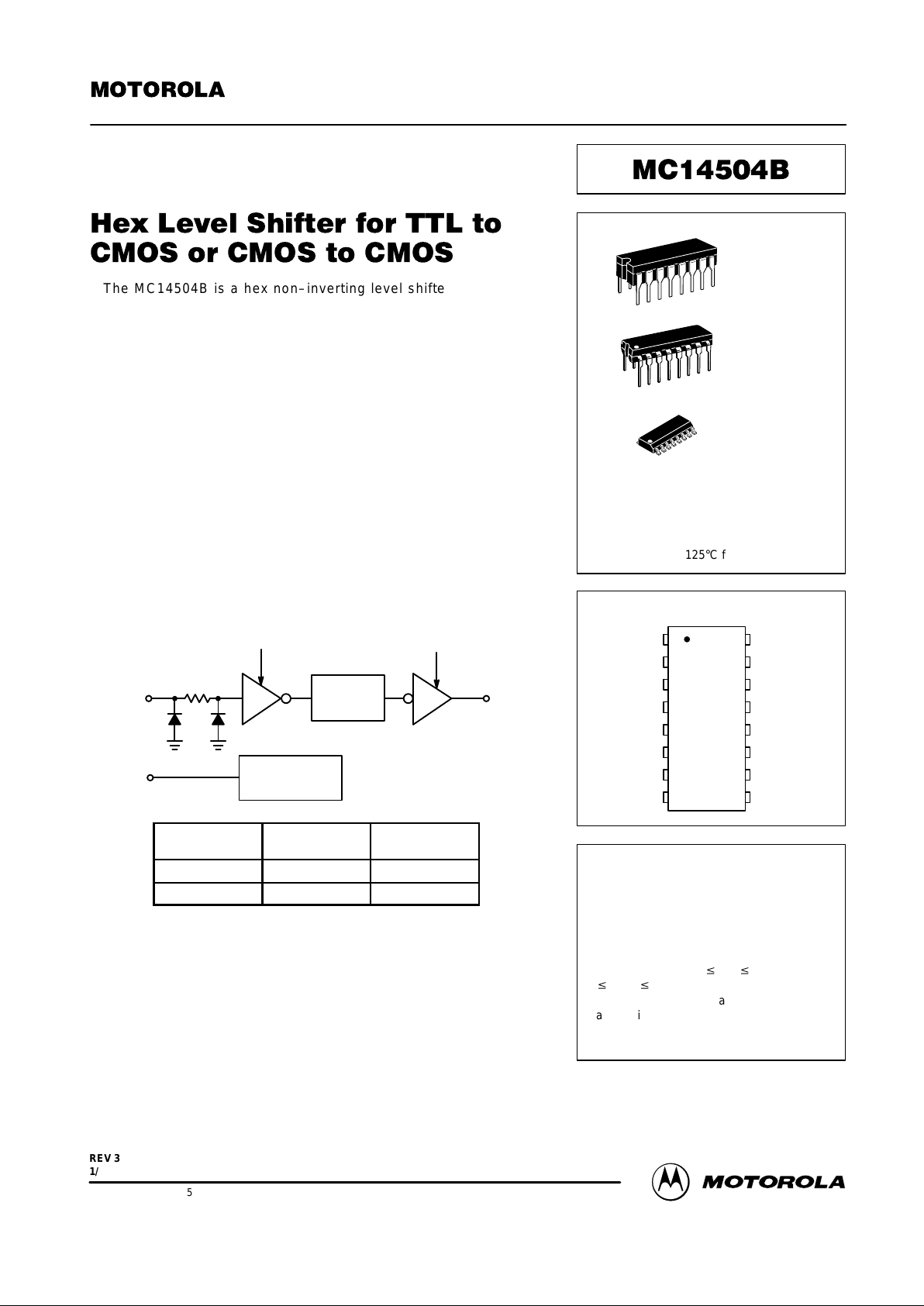
The MC14504B i s a hex non–inverting level shifter using CMOS
technology. The level shifter will shift a TTL signal to CMOS logic levels for
any CMOS supply voltage between 5 and 15 volts. A control input also
allows interface from CMOS to CMOS at one logic level to another logic
level: Either up or down level translating is accomplished by selection of
power supply levels VDD and VCC. The VCC level sets the input signal levels
while VDD selects the output voltage levels.
• UP Translates from a Low to a High Voltage or DOWN Translates from
a High to a Low Voltage
• Input Threshold Can Be Shifted for TTL Compatibility
• No Sequencing Required on Power Supplies or Inputs for Power Up or
Power Down
• 3 to 18 Vdc Operation for VDD and V
CC
• Diode Protected Inputs to V
SS
• Capable of Driving Two Low–Power TTL Loads or One Low–Power
Schottky TTL Load Over the Rated Temperature Range
LOGIC DIAGRAM
INPUT
V
DD
OUTPUT
LEVEL
SHIFTER
MODE
V
CC
TTL/CMOS
MODE SELECT
Mode Select
Input Logic
Levels
Output Logic
Levels
1 (VCC) TTL CMOS
0 (VSS) CMOS CMOS
1/6 of package shown.
SEMICONDUCTOR TECHNICAL DATA
Motorola, Inc. 1995
REV 3
1/94
L SUFFIX
CERAMIC
CASE 620
ORDERING INFORMATION
TA = – 55° to 125°C for all packages.
P SUFFIX
PLASTIC
CASE 648
D SUFFIX
SOIC
CASE 751B
MC14XXXBCP Plastic
MC14XXXBCL Ceramic
MC14XXXBD SOIC
PIN ASSIGNMENT
13
14
15
16
9
10
11
125
4
3
2
1
8
7
6
E
out
MODE
F
in
F
out
V
DD
D
in
D
out
E
in
B
out
A
in
A
out
V
CC
V
SS
C
in
C
out
B
in
This device contains circuitry to protect
the inputs against damage due to high static
voltages or electric fields referenced to the
VSS pin, only. Extra precautions must be
taken to avoid applications of any voltage
higher than maximum rated voltages to this
high–impedance circuit. For proper operation, the ranges VSS v Vin v 18 V and V
SS
v
V
out
v VDD are recommended.
Unused inputs must always be tied to an
appropriate logic voltage level (e.g., either
VSS or VDD). Unused outputs must be left
open.
MOTOROLA CMOS LOGIC DATA
333
MC14504B
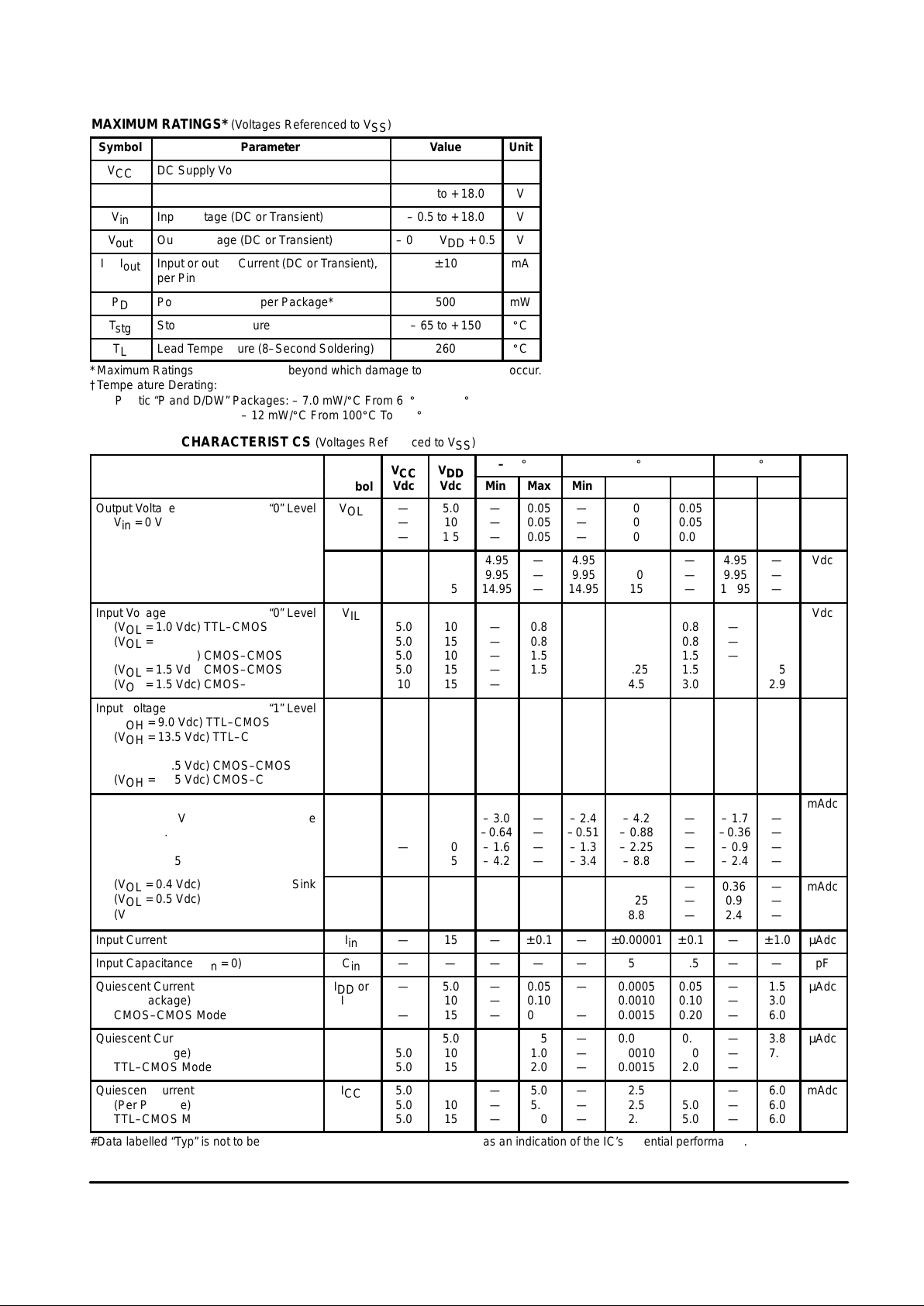
MAXIMUM RATINGS* (Voltages Referenced to V
SS
)
Symbol
Parameter
Value
Unit
V
CC
DC Supply Voltage
– 0.5 to 18.0
V
V
DD
DC Supply Voltage
– 0.5 to + 18.0
V
V
in
Input Voltage (DC or Transient)
– 0.5 to + 18.0
V
V
out
Output Voltage (DC or Transient)
– 0.5 to VDD + 0.5
V
Iin, I
out
Input or output Current (DC or Transient),
per Pin
± 10
mA
P
D
Power Dissipation, per Package*
500
mW
T
stg
Storage Temperature
– 65 to + 150
_
C
T
L
Lead Temperature (8–Second Soldering)
260
_
C
*Maximum Ratings are those values beyond which damage to the device may occur.
†Temperature Derating:
Plastic “P and D/DW” Packages: – 7.0 mW/_C From 65_C To 125_C
Ceramic “L” Packages: – 12 mW/_C From 100_C To 125_C
ELECTRICAL CHARACTERISTICS (Voltages Referenced to V
SS
)
V
V
– 55_C
25_C
125_C
Characteristic
Symbol
V
CC
Vdc
V
DD
Vdc
Min
Max
Min
Typ #
Max
Min
Max
Unit
Output Voltage
“0” Level
Vin = 0 V
V
OL
—
—
—
5.0
10
1 5
—
—
—
0.05
0.05
0.05
—
—
—
0
0
0
0.05
0.05
0.05
—
—
—
0.05
0.05
0.05
Vdc
“1” Level
Vin = V
CC
V
OH
—
—
—
5.0
10
15
4.95
9.95
14.95
—
—
—
4.95
9.95
14.95
5.0
10
15
—
—
—
4.95
9.95
14.95
—
—
—
Vdc
Input Voltage “0” Level
(VOL = 1.0 Vdc) TTL–CMOS
(VOL = 1.5 Vdc) TTL–CMOS
(VOL = 1.0 Vdc) CMOS–CMOS
(VOL = 1.5 Vdc) CMOS–CMOS
(VOL = 1.5 Vdc) CMOS–CMOS
V
IL
5.0
5.0
5.0
5.0
10
10
15
10
15
15
—
—
—
—
—
0.8
0.8
1.5
1.5
3.0
—
—
—
—
—
1.3
1.3
2.25
2.25
4.5
0.8
0.8
1.5
1.5
3.0
—
—
—
—
—
0.8
0.8
1.4
1.5
2.9
Vdc
Input Voltage “1” Level
(VOH = 9.0 Vdc) TTL–CMOS
(VOH = 13.5 Vdc) TTL–CMOS
(VOH = 9.0 Vdc) CMOS–CMOS
(VOH = 13.5 Vdc) CMOS–CMOS
(VOH = 13.5 Vdc) CMOS–CMOS
V
IH
5.0
5.0
5.0
5.0
10
10
15
10
15
15
2.0
2.0
3.6
3.6
7.1
—
—
—
—
—
2.0
2.0
3.5
3.5
7.0
1.5
1.5
2.75
2.75
5.5
—
—
—
—
—
2.0
2.0
3.5
3.5
7.0
—
—
—
—
—
Vdc
Output Drive Current
(VOH = 2.5 Vdc) Source
(VOH = 4.6 Vdc)
(VOH = 9.5 Vdc)
(VOH = 13.5 Vdc)
I
OH
—
—
—
—
5.0
5.0
10
15
– 3.0
–0.64
– 1.6
– 4.2
—
—
—
—
– 2.4
–0.51
– 1.3
– 3.4
– 4.2
– 0.88
– 2.25
– 8.8
—
—
—
—
– 1.7
–0.36
– 0.9
– 2.4
—
—
—
—
mAdc
(VOL = 0.4 Vdc) Sink
(VOL = 0.5 Vdc)
(VOL = 1.5 Vdc)
I
OL
—
—
—
5.0
10
15
0.64
1.6
4.2
—
—
—
0.51
1.3
3.4
0.88
2.25
8.8
—
—
—
0.36
0.9
2.4
—
—
—
mAdc
Input Current
I
in
—
15
—
± 0.1
—
±0.00001
± 0.1
—
± 1.0
µAdc
Input Capacitance (Vin = 0)
C
in
—
—
—
—
—
5.0
7.5
—
—
pF
Quiescent Current
(Per Package)
CMOS–CMOS Mode
IDD or
I
CC
—
—
—
5.0
10
15
—
—
—
0.05
0.10
0.20
—
—
—
0.0005
0.0010
0.0015
0.05
0.10
0.20
—
—
—
1.5
3.0
6.0
µAdc
Quiescent Current
(Per Package)
TTL–CMOS Mode
I
DD
5.0
5.0
5.0
5.0
10
15
—
—
—
0.5
1.0
2.0
—
—
—
0.0005
0.0010
0.0015
0.5
1.0
2.0
—
—
—
3.8
7.5
15
µAdc
Quiescent Current
(Per Package)
TTL–CMOS Mode
I
CC
5.0
5.0
5.0
5.0
10
15
—
—
—
5.0
5.0
5.0
—
—
—
2.5
2.5
2.5
5.0
5.0
5.0
—
—
—
6.0
6.0
6.0
mAdc
#Data labelled “Typ” is not to be used for design purposes but is intended as an indication of the IC’s potential performance.
 Loading...