

MOTOROLA MC145026, MC145027, MC145028, SC41343, SC41344 Technical data
查询145026P供应商
SEMICONDUCTOR TECHNICAL DATA
CMOS
These devices are designed to be used as encoder/decoder pairs in remote
control applications.
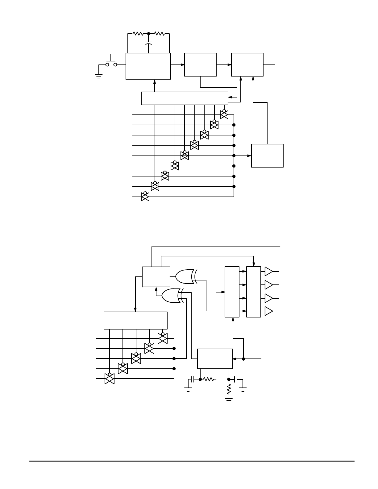
The MC145026 encodes nine lines of information and serially sends this
information upon receipt of a transmit enable (TE
encoded with trinary data (low, high, or open) or binary data (low or high). The
words are transmitted twice per encoding sequence to increase security .
The MC145027 decoder receives the serial stream and interprets five of the
trinary digits as an address code. Thus, 243 addresses are possible. If binary
data is used at the encoder, 32 addresses are possible. The remaining serial
information is interpreted as four bits of binary data. The valid transmission (VT)
output goes high on the MC145027 when two conditions are met. First, two
addresses must be consecutively received (in one encoding sequence) which
both match the local address. Second, the 4 bits of data must match the last
valid data received. The active VT indicates that the information at the Data
output pins has been updated.
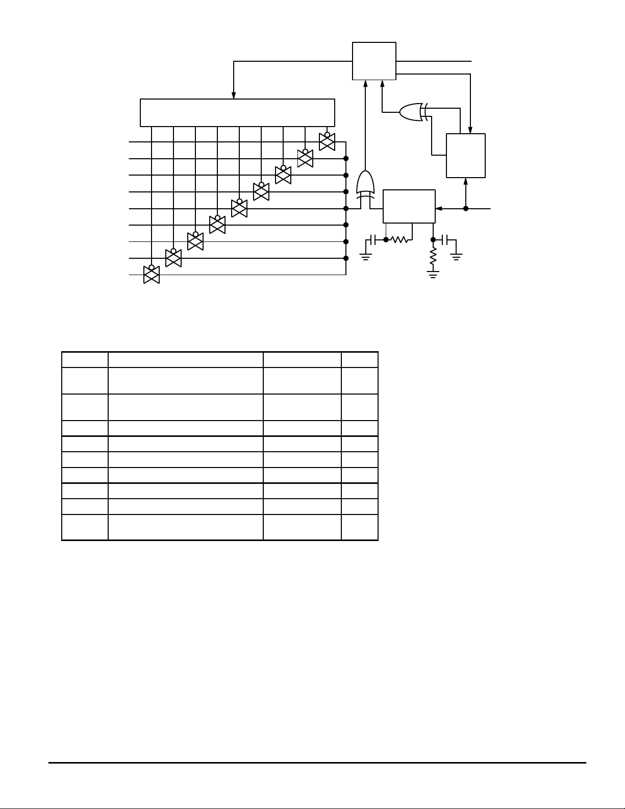
The MC145028 decoder treats all nine trinary digits as an address which
allows 19,683 codes. If binary data is encoded, 512 codes are possible. The VT
output goes high on the MC145028 when two addresses are consecutively
received (in one encoding sequence) which both match the local address.
• Operating Temperature Range: – 40 to + 85°C
• Very–Low Standby Current for the Encoder: 300 nA Maximum @ 25°C
• Interfaces with RF, Ultrasonic, or Infrared Modulators and Demodulators
• RC Oscillator, No Crystal Required
• High External Component Tolerance; Can Use ± 5% Components
• Internal Power–On Reset Forces All Decoder Outputs Low
• Operating Voltage Range: MC145026 = 2.5 to 18 V
MC145027, MC145028 = 4.5 to 18 V
• Low–Voltage Versions Available:
SC41343 = 2.8 to 10 V Version of the MC145027
SC41344 = 2.8 to 10 V Version of the MC145028
• For Infrared Applications, See Application Note AN1016/D
) signal. The nine lines may be
*
Order this document
by MC145026/D
P SUFFIX
PLASTIC DIP
16
1
16
1
16
1
ORDERING INFORMATION
MC145026P Plastic DIP
MC145026D SOG Package
MC145027P, SC41343P Plastic DIP
MC145027DW, SC41343DW SOG Package
MC145028P, SC41344P Plastic DIP
MC145028DW, SC41344DW SOG Package
CASE 648
D SUFFIX
SOG PACKAGE
CASE 751B
DW SUFFIX
SOG PACKAGE
CASE 751G
PIN ASSIGNMENTS
MC145026
ENCODER
A1
1
A2
2
A3
3
A4
4
A5
A6/D6
6
A7/D7
7
V
8
SS
*All MC145026 devices manufactured after date code 9314 or 314 are guaranteed over this wider voltage range. All previous designs using the
low–voltage SC41342 should convert to the MC145026, which is a drop–in replacement. The SC41342 part number has been discontinued.
REV 2
1/98
16
15
14
13
125
11
10
V
DD
D
out
TE
R
TC
C
TC
R
S
A9/D9
9
A8/D8
MC145027/SC41343
DECODERS
1
A1
2
A2
3
A3
4
A4
A5
6
R
1
7
C
1
8
V
SS
16
15
14
13
125
11
10
9
V
DD
D6
D7
D8
D9
VT
R2/C
D
in
2
Motorola, Inc. 1998
MC145028/SC41344
DECODERS
1
A1
2
A2
3
A3
4
A4
A5
6
R
1
7
C
1
8
V
SS
16
15
14
13
125
11
10
9
MC145026•MC145027•MC145028•SC41343•SC41344MOTOROLA
V
DD
A6
A7
A8
A9
VT
R2/C
D
in
2
1
TE
11
14
A1
A2
A3
A4
A5
A6/D6
A7/D7
A8/D8
A9/D9
R
OSCILLA TOR
10
R
S
1
2
3
4
5
6
7
9
TC
C
TC
1312
3–PIN
AND
ENABLE
RING COUNTER AND 1–OF–9 DECODER
9
87654321
÷
4
DIVIDER
DATA SELECT
AND
BUFFER
TRINARY
DETECTOR
VDD = PIN 16
VSS = PIN 8
15
D
out
A1
A2
A3
A4
A5
Figure 1. MC145026 Encoder Block Diagram
CONTROL
LOGIC
SEQUENCER CIRCUIT
54321
1
2
3
4
5
DATA
EXTRACTOR
C
1
76
10
R
1
4–BIT SHIFT REGISTER
C
2
R
2
11
15
14
LATCH
VDD = PIN 16
VSS = PIN 8
13
12
9
D
in
VT
D6
D7
D8
D9
Figure 2. MC145027 Decoder Block Diagram
MC145026•MC145027•MC145028•SC41343•SC41344 MOTOROLA
2
A1
A2
A3
A4
A5
A6
A7
A8
A9
SEQUENCER CIRCUIT
987654321
1
2
3
4
5
15
14
13
12
Figure 3. MC145028 Decoder Block Diagram
CONTROL
LOGIC
DATA
EXTRACTOR
C
1
76
R
1
10
11
9–BIT
SHIFT
REGISTER
C
2
R
2
VT
9
D
in
VDD = PIN 16
VSS = PIN 8
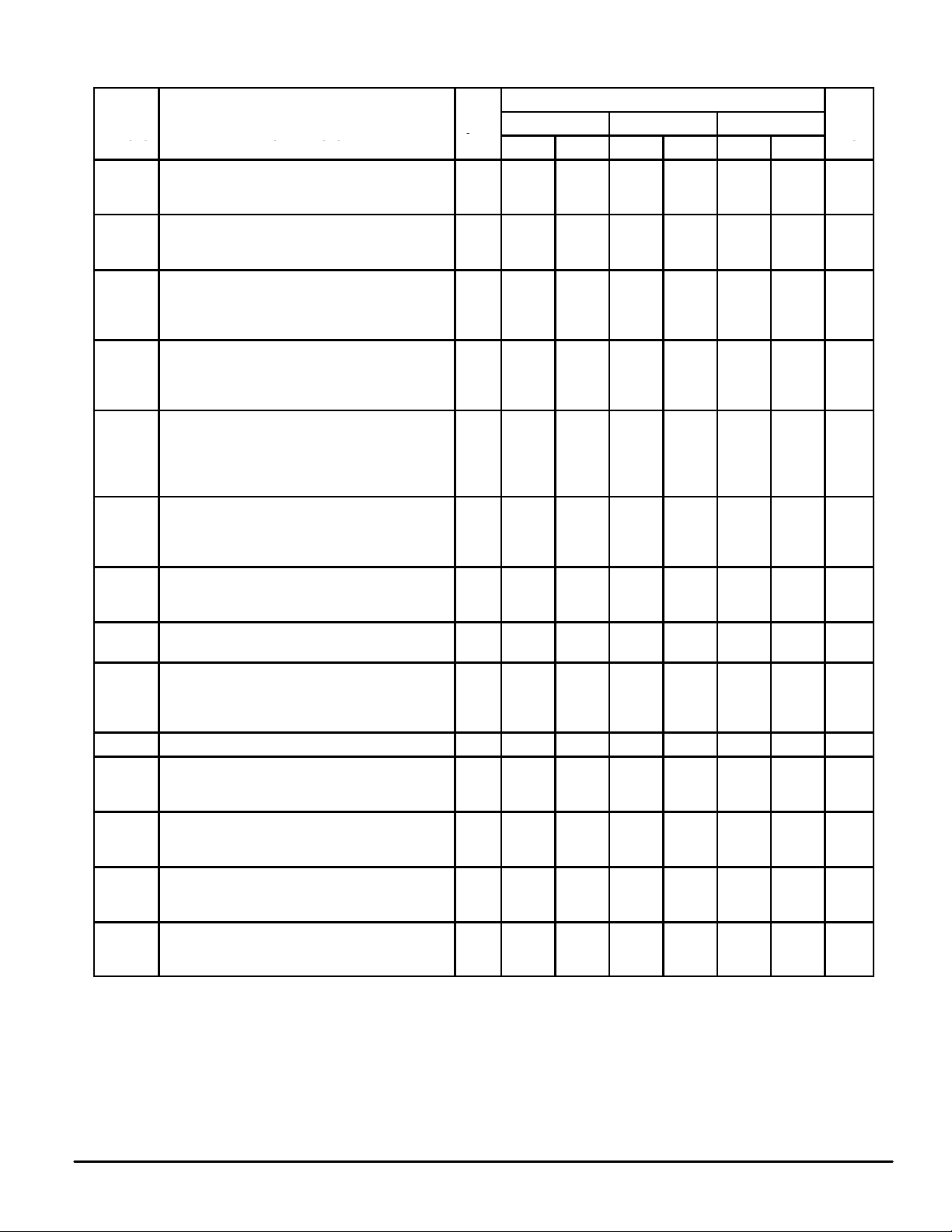
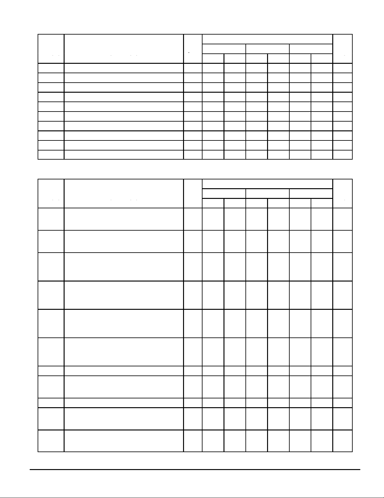
MAXIMUM RATINGS* (Voltages Referenced to V
Rating Symbol Value Unit
V
V
V
V
I
I
out
P
T
T
*Maximum Ratings are those values beyond which damage to the device may occur. Func-
tional operation should be restricted to the limits in the Electrical Characteristics tables or
Pin Descriptions section.
DC Supply Voltage (except SC41343,
DD
SC41344)
DC Supply Voltage (SC41343, SC41344
DD
only)
DC Input Voltage – 0.5 to VDD + 0.5 V
in
DC Output Voltage – 0.5 to VDD + 0.5 V
out
DC Input Current, per Pin ± 10 mA
in
DC Output Current, per Pin ± 10 mA
Power Dissipation, per Package 500 mW
D
Storage Temperature – 65 to + 150 °C
stg
Lead Temperature, 1 mm from Case for
L
10 Seconds
)
SS
– 0.5 to + 18 V
– 0.5 to + 10 V
260 °C
This device contains protection circuitry to
guard against damage due to high static
voltages or electric fields. However, precautions must be taken to avoid applications of any
voltage higher than maximum rated voltages
to this high–impedance circuit. For proper
operation, Vin and V
to the range VSS ≤ (Vin or V
should be constrained
out
) ≤ VDD.
out
MC145026•MC145027•MC145028•SC41343•SC41344MOTOROLA
3
ELECTRICAL CHARACTERISTICS — MC145026*, MC145027, and MC145028 (Voltage Referenced to V
V
DD
Guaranteed Limit
– 40°C 25°C 85°C
Min Max Min Max Min Max
—
—
—
4.95
9.95
14.95
—
—
—
3.5
7.0
11
– 2.5
– 0.52
– 1.3
– 3.6
0.52
1.3
3.6
—
—
—
—
—
—
—
—
—
—
—
—
—
—
—
—
—
—
0.05
0.05
0.05
—
—
—
1.5
3.0
4.0
—
—
—
—
—
—
—
—
—
—
—
—
—
—
—
—
—
—
—
—
—
—
—
—
—
—
—
—
—
—
—
4.95
9.95
14.95
—
—
—
3.5
7.0
11
– 2.1
– 0.44
– 1.1
– 3.0
0.44
1.1
3.0
3.0
16
35
—
—
—
—
—
—
—
—
—
—
—
—
—
—
—
0.05
0.05
0.05
—
—
—
1.5
3.0
4.0
—
—
—
—
—
—
—
—
—
—
11
60
120
± 110
± 500
± 1000
0.1
0.2
0.3
50
100
150
200
400
600
400
800
1200
Symbol Characteristic
V
V
V
V
I
OH
I
C
I
I
I
I
*Also see next Electrical Characteristics table for 2.5 V specifications.
Low–Level Output Voltage (Vin = VDD or 0) 5.0
OL
High–Level Output Voltage (Vin = 0 or VDD) 5.0
OH
Low–Level Input Voltage
IL
High–Level Input Voltage
IH
High–Level Output Current
Low–Level Output Current
OL
I
Input Current — TE
in
(MC145026, Pull–Up Device)
I
Input Current
in
RS (MC145026), Din (MC145027, MC145028)
I
Input Current
in
in
DD
DD
dd
dd
A1 – A5, A6/D6 – A9/D9 (MC145026),
A1 – A5 (MC145027),
A1 – A9 (MC145028)
Input Capacitance (Vin = 0) — — — — 7.5 — — pF
Quiescent Current — MC145026 5.0
Quiescent Current — MC145027, MC145028 5.0
Dynamic Supply Current — MC145026
(fc = 20 kHz)
Dynamic Supply Current — MC145027, MC145028
(fc = 20 kHz)
(V
= 4.5 or 0.5 V)
out
(V
= 9.0 or 1.0 V)
out
(V
= 13.5 or 1.5 V)
out
(V
= 0.5 or 4.5 V)
out
(V
= 1.0 or 9.0 V)
out
(V
= 1.5 or 13.5 V)
out
(V
(V
(V
(V
out
(V
(V
(V
= 2.5 V)
out
= 4.6 V)
out
= 9.5 V)
out
= 13.5 V)
= 0.4 V)
out
= 0.5 V)
out
= 1.5 V)
out
V
V
10
15
10
15
5.0
10
15
5.0
10
15
5.0
5.0
10
15
5.0
10
15
5.0
10
15
15 — ± 0.3 — ± 0.3 — ± 1.0 µA
5.0
10
15
10
15
10
15
5.0
10
15
5.0
10
15
SS
—
—
—
4.95
9.95
14.95
—
—
—
3.5
7.0
11
– 1.7
– 0.36
– 0.9
– 2.4
0.36
0.9
2.4
—
—
—
—
—
—
—
—
—
—
—
—
—
—
—
—
—
—
)
Unit
0.05
0.05
0.05
—
—
—
1.5
3.0
4.0
—
—
—
—
—
—
—
—
—
—
—
—
—
—
—
—
—
—
—
—
—
—
—
—
—
—
—
—
V
V
V
V
mA
mA
µA
µA
µA
µA
µA
µA
MC145026•MC145027•MC145028•SC41343•SC41344 MOTOROLA
4
ELECTRICAL CHARACTERISTICS — MC145026 (Voltage Referenced to V
V
DD
V
DD
– 40°C 25°C 85°C
Min Max Min Max Min Max
Symbol Characteristic
V
V
V
V
I
OH
I
I
I
Low–Level Output Voltage (Vin = 0 V or VDD) 2.5 — 0.05 — 0.05 — 0.05 V
OL
High–Level Output Voltage (Vin = 0 V or VDD) 2.5 2.45 — 2.45 — 2.45 — V
OH
Low–Level Input Voltage (V
IL
High–Level Input Voltage (V
IH
High–Level Output Current (V
Low–Level Output Current (V
OL
I
Input Current (TE — Pull–Up Device) 2.5 — — 0.09 1.8 — — µA
in
I
Input Current (A1–A5, A6/D6–A9/D9) 2.5 — — — ± 25 — — µA
in
Quiescent Current 2.5 — — — 0.05 — — µA
DD
Dynamic Supply Current (fc = 20 kHz) 2.5 — — — 40 — — µA
dd
V
V
= 0.5 V or 2.0 V) 2.5 — 0.3 — 0.3 — 0.3 V
out
= 0.5 V or 2.0 V) 2.5 2.2 — 2.2 — 2.2 — V
out
= 1.25 V) 2.5 0.28 — 0.25 — 0.2 — mA
out
= 0.4 V) 2.5 0.22 — 0.2 — 0.16 — mA
out
SS
)
Guaranteed Limit
Unit
ELECTRICAL CHARACTERISTICS — SC41343 and SC41344 (Voltage Referenced to V
Guaranteed Limit
– 40°C 25°C 85°C
Min Max Min Max Min Max
—
—
—
2.75
4.95
9.95
—
—
—
1.96
3.5
7.0
– 0.73
– 0.59
– 1.3
0.35
0.8
3.5
—
—
—
—
—
—
—
—
—
0.05
0.05
0.05
—
—
—
0.84
1.5
3.0
—
—
—
—
—
—
—
—
—
—
—
—
—
—
—
—
—
—
– 0.7
– 0.5
– 1.1
Symbol Characteristic
V
V
V
V
I
OH
I
C
I
I
Low–Level Output Voltage (Vin = 0 V or VDD) 2.8
OL
High–Level Output Voltage (Vin = 0 V or VDD) 2.8
OH
Low–Level Input Voltage
IL
High–Level Input Voltage
IH
High–Level Output Current
Low–Level Output Current
OL
I
Input Current — D
in
I
Input Current
in
in
DD
dd
A1 – A5 (SC41343)
A1 – A9 (SC41344)
Input Capacitance (Vin = 0) — — — — 7.5 — — pF
Quiescent Current 2.8
Dynamic Supply Current (fc = 20 kHz) 2.8
in
(V
(V
(V
(V
(V
(V
= 2.3 V or 0.5 V)
out
= 4.5 V or 0.5 V)
out
= 9.0 V or 1.0 V)
out
= 0.5 V or 2.3 V)
out
= 0.5 V or 4.5 V)
out
= 1.0 V or 9.0 V)
out
(V
= 1.4 V)
out
(V
= 4.5 V)
out
(V
= 9.0 V)
out
(V
= 0.4 V)
out
(V
= 0.5 V)
out
(V
= 1.0 V)
out
V
V
5.0
10
5.0
10
2.8
5.0
10
2.8
5.0
10
2.8
5.0
10
2.8
5.0
10
10 — ± 0.3 — ± 0.3 — ± 1.0 µA
2.8
5.0
10
5.0
10
5.0
10
SS
—
—
—
2.75
4.95
9.95
—
—
—
1.96
3.5
7.0
0.3
0.6
2.9
—
—
—
—
—
—
—
—
—
)
Unit
0.05
0.05
0.05
—
—
—
0.84
1.5
3.0
—
—
—
—
—
—
—
—
—
± 30
± 140
± 600
60
75
150
300
500
1000
—
—
—
2.75
4.95
9.95
—
—
—
1.96
3.5
7.0
– 0.55
– 0.41
– 0.9
0.24
0.4
2.3
—
—
—
—
—
—
—
—
—
0.05
0.05
0.05
—
—
—
0.84
1.5
3.0
—
—
—
—
—
—
—
—
—
—
—
—
—
—
—
—
—
—
V
V
V
V
mA
mA
µA
µA
µA
MC145026•MC145027•MC145028•SC41343•SC41344MOTOROLA
5
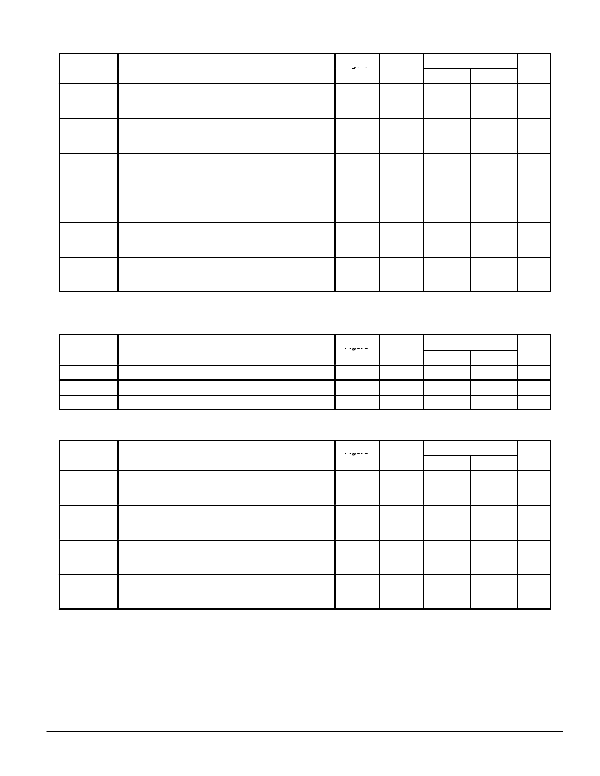
SWITCHING CHARACTERISTICS — MC145026*, MC145027, and MC145028 (C
Figure
Figure
Figure
Figure
Symbol Characteristic
t
, t
TLH
t
r
t
f
f
osc
f Decoder Frequency — Referenced to Encoder Clock 12 5.0
t
w
*Also see next Switching Characteristics table for 2.5 V specifications.
Output Transition Time 4,8 5.0
THL
Din Rise Time — Decoders 5 5.0
Din Fall Time — Decoders 5 5.0
Encoder Clock Frequency 6 5.0
TE Pulse Width — Encoders 7 5.0
No.
= 50 pF, TA = 25°C)
L
Guaranteed Limit
V
DD
10
15
10
15
10
15
10
15
10
15
10
15
0.001
0.001
0.001
Min Max
—
—
—
—
—
—
—
—
—
1.0
1.0
1.0
65
30
20
200
100
80
15
15
15
15
5.0
4.0
2.0
5.0
10
240
410
450
—
—
—
Unit
ns
µs
µs
MHz
kHz
ns
SWITCHING CHARACTERISTICS — MC145026 (C
Symbol Characteristic
t
TLH
f
, t
osc
t
w
Output Transition Time 4, 8 2.5 — 450 ns
THL
Encoder Clock Frequency 6 2.5 1.0 250 kHz
TE Pulse Width 7 2.5 1.5 — µs
SWITCHING CHARACTERISTICS — SC41343 and SC41344 (C
Symbol Characteristic
t
, t
TLH
t
r
t
f
f Decoder Frequency — Referenced to Encoder Clock 12 2.8
Output Transition Time 4, 8 2.8
THL
Din Rise Time 5 2.8
Din Fall Time 5 2.8
= 50 pF, TA = 25°C)
L
= 50 pF, TA = 25°C)
L
Figure
Figure
No.
No.
V
V
DD
DD
5.0
10
5.0
10
5.0
10
5.0
10
Guaranteed Limit
Min Max
Guaranteed Limit
Min Max
—
—
—
—
—
—
—
—
—
1.0
1.0
1.0
320
200
100
15
15
15
15
15
5.0
100
240
410
Unit
Unit
ns
µs
µs
kHz
MC145026•MC145027•MC145028•SC41343•SC41344 MOTOROLA
6
 Loading...