

查询145026P供应商
SEMICONDUCTOR TECHNICAL DATA
CMOS
These devices are designed to be used as encoder/decoder pairs in remote
control applications.
The MC145026 encodes nine lines of information and serially sends this
information upon receipt of a transmit enable (TE
encoded with trinary data (low, high, or open) or binary data (low or high). The
words are transmitted twice per encoding sequence to increase security .
The MC145027 decoder receives the serial stream and interprets five of the
trinary digits as an address code. Thus, 243 addresses are possible. If binary
data is used at the encoder, 32 addresses are possible. The remaining serial
information is interpreted as four bits of binary data. The valid transmission (VT)
output goes high on the MC145027 when two conditions are met. First, two
addresses must be consecutively received (in one encoding sequence) which
both match the local address. Second, the 4 bits of data must match the last
valid data received. The active VT indicates that the information at the Data
output pins has been updated.
The MC145028 decoder treats all nine trinary digits as an address which
allows 19,683 codes. If binary data is encoded, 512 codes are possible. The VT
output goes high on the MC145028 when two addresses are consecutively
received (in one encoding sequence) which both match the local address.
• Operating Temperature Range: – 40 to + 85°C
• Very–Low Standby Current for the Encoder: 300 nA Maximum @ 25°C
• Interfaces with RF, Ultrasonic, or Infrared Modulators and Demodulators
• RC Oscillator, No Crystal Required
• High External Component Tolerance; Can Use ± 5% Components
• Internal Power–On Reset Forces All Decoder Outputs Low
• Operating Voltage Range: MC145026 = 2.5 to 18 V
MC145027, MC145028 = 4.5 to 18 V
• Low–Voltage Versions Available:
SC41343 = 2.8 to 10 V Version of the MC145027
SC41344 = 2.8 to 10 V Version of the MC145028
• For Infrared Applications, See Application Note AN1016/D
) signal. The nine lines may be
*
Order this document
by MC145026/D
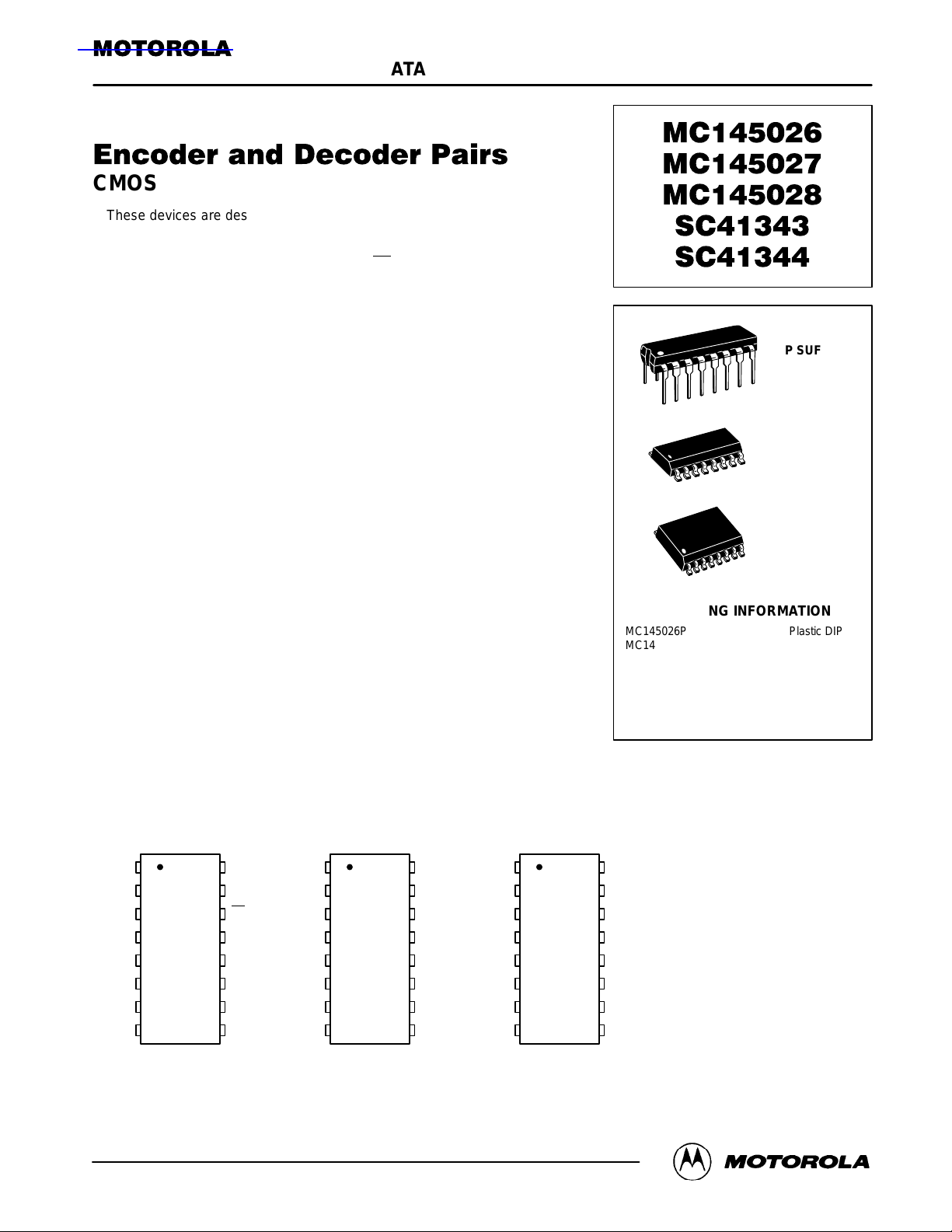
P SUFFIX
PLASTIC DIP
16
1
16
1
16
1
ORDERING INFORMATION
MC145026P Plastic DIP
MC145026D SOG Package
MC145027P, SC41343P Plastic DIP
MC145027DW, SC41343DW SOG Package
MC145028P, SC41344P Plastic DIP
MC145028DW, SC41344DW SOG Package
CASE 648
D SUFFIX
SOG PACKAGE
CASE 751B
DW SUFFIX
SOG PACKAGE
CASE 751G
PIN ASSIGNMENTS
MC145026
ENCODER
A1
1
A2
2
A3
3
A4
4
A5
A6/D6
6
A7/D7
7
V
8
SS
*All MC145026 devices manufactured after date code 9314 or 314 are guaranteed over this wider voltage range. All previous designs using the
low–voltage SC41342 should convert to the MC145026, which is a drop–in replacement. The SC41342 part number has been discontinued.
REV 2
1/98
16
15
14
13
125
11
10
V
DD
D
out
TE
R
TC
C
TC
R
S
A9/D9
9
A8/D8
MC145027/SC41343
DECODERS
1
A1
2
A2
3
A3
4
A4
A5
6
R
1
7
C
1
8
V
SS
16
15
14
13
125
11
10
9
V
DD
D6
D7
D8
D9
VT
R2/C
D
in
2
Motorola, Inc. 1998
MC145028/SC41344
DECODERS
1
A1
2
A2
3
A3
4
A4
A5
6
R
1
7
C
1
8
V
SS
16
15
14
13
125
11
10
9
MC145026•MC145027•MC145028•SC41343•SC41344MOTOROLA
V
DD
A6
A7
A8
A9
VT
R2/C
D
in
2
1
TE
11
14
A1
A2
A3
A4
A5
A6/D6
A7/D7
A8/D8
A9/D9
R
OSCILLA TOR
10
R
S
1
2
3
4
5
6
7
9
TC
C
TC
1312
3–PIN
AND
ENABLE
RING COUNTER AND 1–OF–9 DECODER
9
87654321
÷
4
DIVIDER
DATA SELECT
AND
BUFFER
TRINARY
DETECTOR
VDD = PIN 16
VSS = PIN 8
15
D
out
A1
A2
A3
A4
A5
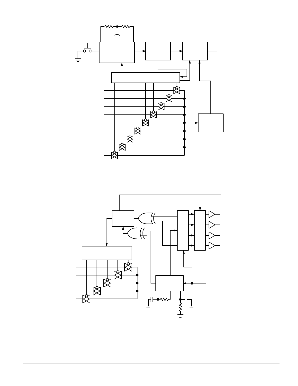
Figure 1. MC145026 Encoder Block Diagram
CONTROL
LOGIC
SEQUENCER CIRCUIT
54321
1
2
3
4
5
DATA
EXTRACTOR
C
1
76
10
R
1
4–BIT SHIFT REGISTER
C
2
R
2
11
15
14
LATCH
VDD = PIN 16
VSS = PIN 8
13
12
9
D
in
VT
D6
D7
D8
D9
Figure 2. MC145027 Decoder Block Diagram
MC145026•MC145027•MC145028•SC41343•SC41344 MOTOROLA
2
A1
A2
A3
A4
A5
A6
A7
A8
A9
SEQUENCER CIRCUIT
987654321
1
2
3
4
5
15
14
13
12
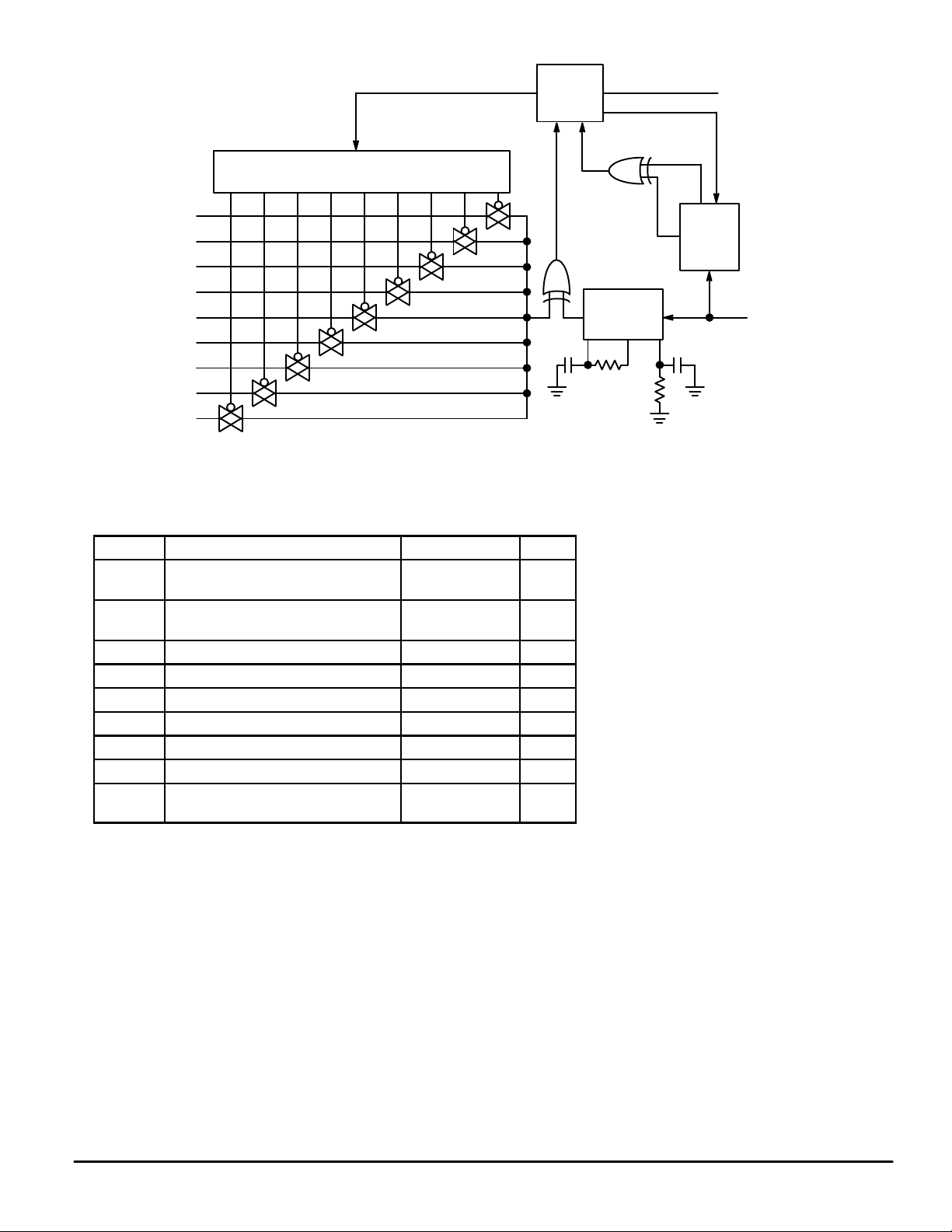
Figure 3. MC145028 Decoder Block Diagram
CONTROL
LOGIC
DATA
EXTRACTOR
C
1
76
R
1
10
11
9–BIT
SHIFT
REGISTER
C
2
R
2
VT
9
D
in
VDD = PIN 16
VSS = PIN 8
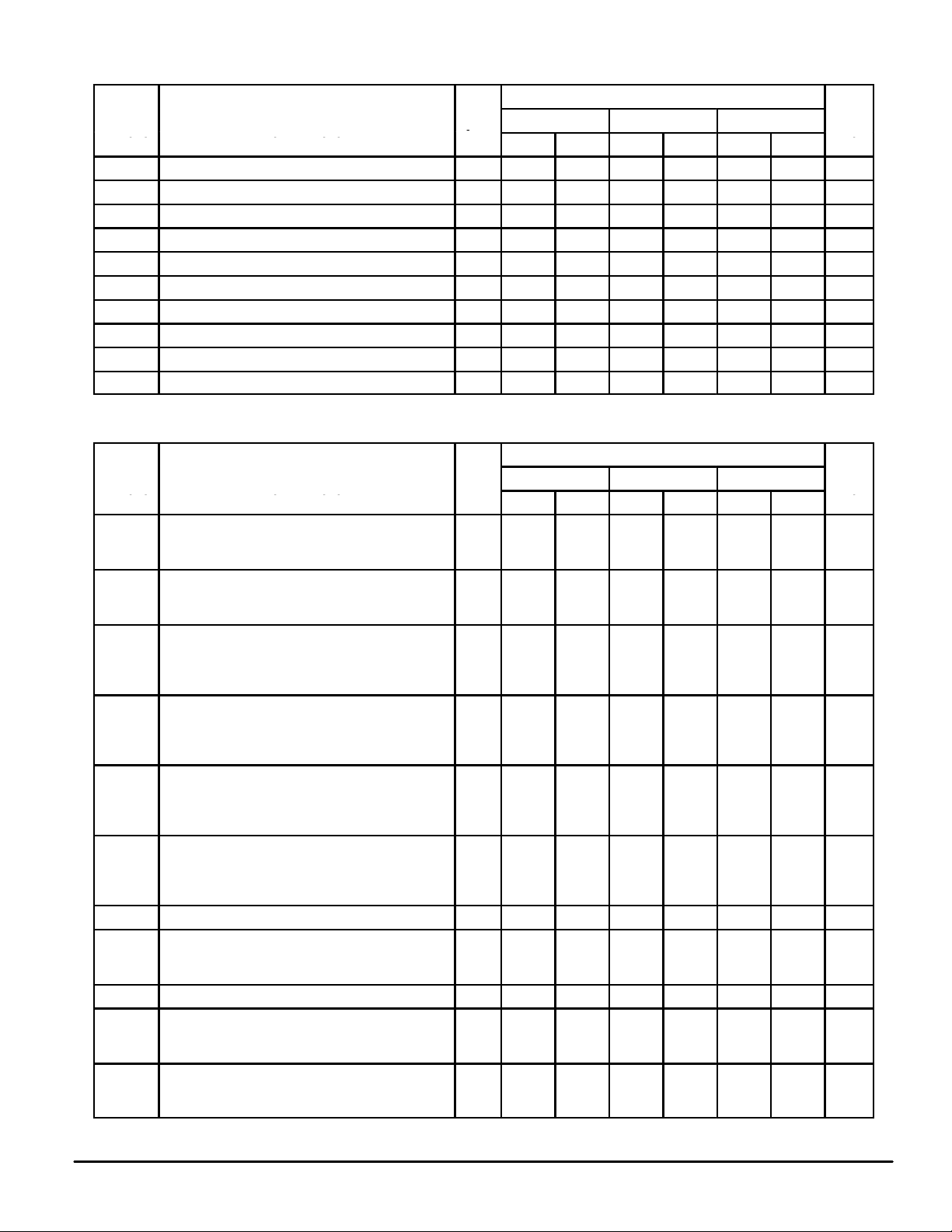
MAXIMUM RATINGS* (Voltages Referenced to V
Rating Symbol Value Unit
V
V
V
V
I
I
out
P
T
T
*Maximum Ratings are those values beyond which damage to the device may occur. Func-
tional operation should be restricted to the limits in the Electrical Characteristics tables or
Pin Descriptions section.
DC Supply Voltage (except SC41343,
DD
SC41344)
DC Supply Voltage (SC41343, SC41344
DD
only)
DC Input Voltage – 0.5 to VDD + 0.5 V
in
DC Output Voltage – 0.5 to VDD + 0.5 V
out
DC Input Current, per Pin ± 10 mA
in
DC Output Current, per Pin ± 10 mA
Power Dissipation, per Package 500 mW
D
Storage Temperature – 65 to + 150 °C
stg
Lead Temperature, 1 mm from Case for
L
10 Seconds
)
SS
– 0.5 to + 18 V
– 0.5 to + 10 V
260 °C
This device contains protection circuitry to
guard against damage due to high static
voltages or electric fields. However, precautions must be taken to avoid applications of any
voltage higher than maximum rated voltages
to this high–impedance circuit. For proper
operation, Vin and V
to the range VSS ≤ (Vin or V
should be constrained
out
) ≤ VDD.
out
MC145026•MC145027•MC145028•SC41343•SC41344MOTOROLA
3

ELECTRICAL CHARACTERISTICS — MC145026*, MC145027, and MC145028 (Voltage Referenced to V
V
DD
Guaranteed Limit
– 40°C 25°C 85°C
Min Max Min Max Min Max
—
—
—
4.95
9.95
14.95
—
—
—
3.5
7.0
11
– 2.5
– 0.52
– 1.3
– 3.6
0.52
1.3
3.6
—
—
—
—
—
—
—
—
—
—
—
—
—
—
—
—
—
—
0.05
0.05
0.05
—
—
—
1.5
3.0
4.0
—
—
—
—
—
—
—
—
—
—
—
—
—
—
—
—
—
—
—
—
—
—
—
—
—
—
—
—
—
—
—
4.95
9.95
14.95
—
—
—
3.5
7.0
11
– 2.1
– 0.44
– 1.1
– 3.0
0.44
1.1
3.0
3.0
16
35
—
—
—
—
—
—
—
—
—
—
—
—
—
—
—
0.05
0.05
0.05
—
—
—
1.5
3.0
4.0
—
—
—
—
—
—
—
—
—
—
11
60
120
± 110
± 500
± 1000
0.1
0.2
0.3
50
100
150
200
400
600
400
800
1200
Symbol Characteristic
V
V
V
V
I
OH
I
C
I
I
I
I
*Also see next Electrical Characteristics table for 2.5 V specifications.
Low–Level Output Voltage (Vin = VDD or 0) 5.0
OL
High–Level Output Voltage (Vin = 0 or VDD) 5.0
OH
Low–Level Input Voltage
IL
High–Level Input Voltage
IH
High–Level Output Current
Low–Level Output Current
OL
I
Input Current — TE
in
(MC145026, Pull–Up Device)
I
Input Current
in
RS (MC145026), Din (MC145027, MC145028)
I
Input Current
in
in
DD
DD
dd
dd
A1 – A5, A6/D6 – A9/D9 (MC145026),
A1 – A5 (MC145027),
A1 – A9 (MC145028)
Input Capacitance (Vin = 0) — — — — 7.5 — — pF
Quiescent Current — MC145026 5.0
Quiescent Current — MC145027, MC145028 5.0
Dynamic Supply Current — MC145026
(fc = 20 kHz)
Dynamic Supply Current — MC145027, MC145028
(fc = 20 kHz)
(V
= 4.5 or 0.5 V)
out
(V
= 9.0 or 1.0 V)
out
(V
= 13.5 or 1.5 V)
out
(V
= 0.5 or 4.5 V)
out
(V
= 1.0 or 9.0 V)
out
(V
= 1.5 or 13.5 V)
out
(V
(V
(V
(V
out
(V
(V
(V
= 2.5 V)
out
= 4.6 V)
out
= 9.5 V)
out
= 13.5 V)
= 0.4 V)
out
= 0.5 V)
out
= 1.5 V)
out
V
V
10
15
10
15
5.0
10
15
5.0
10
15
5.0
5.0
10
15
5.0
10
15
5.0
10
15
15 — ± 0.3 — ± 0.3 — ± 1.0 µA
5.0
10
15
10
15
10
15
5.0
10
15
5.0
10
15
SS
—
—
—
4.95
9.95
14.95
—
—
—
3.5
7.0
11
– 1.7
– 0.36
– 0.9
– 2.4
0.36
0.9
2.4
—
—
—
—
—
—
—
—
—
—
—
—
—
—
—
—
—
—
)
Unit
0.05
0.05
0.05
—
—
—
1.5
3.0
4.0
—
—
—
—
—
—
—
—
—
—
—
—
—
—
—
—
—
—
—
—
—
—
—
—
—
—
—
—
V
V
V
V
mA
mA
µA
µA
µA
µA
µA
µA
MC145026•MC145027•MC145028•SC41343•SC41344 MOTOROLA
4
ELECTRICAL CHARACTERISTICS — MC145026 (Voltage Referenced to V
V
DD
V
DD
– 40°C 25°C 85°C
Min Max Min Max Min Max
Symbol Characteristic
V
V
V
V
I
OH
I
I
I
Low–Level Output Voltage (Vin = 0 V or VDD) 2.5 — 0.05 — 0.05 — 0.05 V
OL
High–Level Output Voltage (Vin = 0 V or VDD) 2.5 2.45 — 2.45 — 2.45 — V
OH
Low–Level Input Voltage (V
IL
High–Level Input Voltage (V
IH
High–Level Output Current (V
Low–Level Output Current (V
OL
I
Input Current (TE — Pull–Up Device) 2.5 — — 0.09 1.8 — — µA
in
I
Input Current (A1–A5, A6/D6–A9/D9) 2.5 — — — ± 25 — — µA
in
Quiescent Current 2.5 — — — 0.05 — — µA
DD
Dynamic Supply Current (fc = 20 kHz) 2.5 — — — 40 — — µA
dd
V
V
= 0.5 V or 2.0 V) 2.5 — 0.3 — 0.3 — 0.3 V
out
= 0.5 V or 2.0 V) 2.5 2.2 — 2.2 — 2.2 — V
out
= 1.25 V) 2.5 0.28 — 0.25 — 0.2 — mA
out
= 0.4 V) 2.5 0.22 — 0.2 — 0.16 — mA
out
SS
)
Guaranteed Limit
Unit
ELECTRICAL CHARACTERISTICS — SC41343 and SC41344 (Voltage Referenced to V
Guaranteed Limit
– 40°C 25°C 85°C
Min Max Min Max Min Max
—
—
—
2.75
4.95
9.95
—
—
—
1.96
3.5
7.0
– 0.73
– 0.59
– 1.3
0.35
0.8
3.5
—
—
—
—
—
—
—
—
—
0.05
0.05
0.05
—
—
—
0.84
1.5
3.0
—
—
—
—
—
—
—
—
—
—
—
—
—
—
—
—
—
—
– 0.7
– 0.5
– 1.1
Symbol Characteristic
V
V
V
V
I
OH
I
C
I
I
Low–Level Output Voltage (Vin = 0 V or VDD) 2.8
OL
High–Level Output Voltage (Vin = 0 V or VDD) 2.8
OH
Low–Level Input Voltage
IL
High–Level Input Voltage
IH
High–Level Output Current
Low–Level Output Current
OL
I
Input Current — D
in
I
Input Current
in
in
DD
dd
A1 – A5 (SC41343)
A1 – A9 (SC41344)
Input Capacitance (Vin = 0) — — — — 7.5 — — pF
Quiescent Current 2.8
Dynamic Supply Current (fc = 20 kHz) 2.8
in
(V
(V
(V
(V
(V
(V
= 2.3 V or 0.5 V)
out
= 4.5 V or 0.5 V)
out
= 9.0 V or 1.0 V)
out
= 0.5 V or 2.3 V)
out
= 0.5 V or 4.5 V)
out
= 1.0 V or 9.0 V)
out
(V
= 1.4 V)
out
(V
= 4.5 V)
out
(V
= 9.0 V)
out
(V
= 0.4 V)
out
(V
= 0.5 V)
out
(V
= 1.0 V)
out
V
V
5.0
10
5.0
10
2.8
5.0
10
2.8
5.0
10
2.8
5.0
10
2.8
5.0
10
10 — ± 0.3 — ± 0.3 — ± 1.0 µA
2.8
5.0
10
5.0
10
5.0
10
SS
—
—
—
2.75
4.95
9.95
—
—
—
1.96
3.5
7.0
0.3
0.6
2.9
—
—
—
—
—
—
—
—
—
)
Unit
0.05
0.05
0.05
—
—
—
0.84
1.5
3.0
—
—
—
—
—
—
—
—
—
± 30
± 140
± 600
60
75
150
300
500
1000
—
—
—
2.75
4.95
9.95
—
—
—
1.96
3.5
7.0
– 0.55
– 0.41
– 0.9
0.24
0.4
2.3
—
—
—
—
—
—
—
—
—
0.05
0.05
0.05
—
—
—
0.84
1.5
3.0
—
—
—
—
—
—
—
—
—
—
—
—
—
—
—
—
—
—
V
V
V
V
mA
mA
µA
µA
µA
MC145026•MC145027•MC145028•SC41343•SC41344MOTOROLA
5
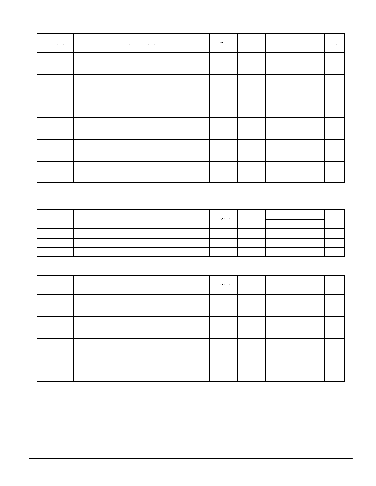
SWITCHING CHARACTERISTICS — MC145026*, MC145027, and MC145028 (C
Figure
Figure
Figure
Figure
Symbol Characteristic
t
, t
TLH
t
r
t
f
f
osc
f Decoder Frequency — Referenced to Encoder Clock 12 5.0
t
w
*Also see next Switching Characteristics table for 2.5 V specifications.
Output Transition Time 4,8 5.0
THL
Din Rise Time — Decoders 5 5.0
Din Fall Time — Decoders 5 5.0
Encoder Clock Frequency 6 5.0
TE Pulse Width — Encoders 7 5.0
No.
= 50 pF, TA = 25°C)
L
Guaranteed Limit
V
DD
10
15
10
15
10
15
10
15
10
15
10
15
0.001
0.001
0.001
Min Max
—
—
—
—
—
—
—
—
—
1.0
1.0
1.0
65
30
20
200
100
80
15
15
15
15
5.0
4.0
2.0
5.0
10
240
410
450
—
—
—
Unit
ns
µs
µs
MHz
kHz
ns
SWITCHING CHARACTERISTICS — MC145026 (C
Symbol Characteristic
t
TLH
f
, t
osc
t
w
Output Transition Time 4, 8 2.5 — 450 ns
THL
Encoder Clock Frequency 6 2.5 1.0 250 kHz
TE Pulse Width 7 2.5 1.5 — µs
SWITCHING CHARACTERISTICS — SC41343 and SC41344 (C
Symbol Characteristic
t
, t
TLH
t
r
t
f
f Decoder Frequency — Referenced to Encoder Clock 12 2.8
Output Transition Time 4, 8 2.8
THL
Din Rise Time 5 2.8
Din Fall Time 5 2.8
= 50 pF, TA = 25°C)
L
= 50 pF, TA = 25°C)
L
Figure
Figure
No.
No.
V
V
DD
DD
5.0
10
5.0
10
5.0
10
5.0
10
Guaranteed Limit
Min Max
Guaranteed Limit
Min Max
—
—
—
—
—
—
—
—
—
1.0
1.0
1.0
320
200
100
15
15
15
15
15
5.0
100
240
410
Unit
Unit
ns
µs
µs
kHz
MC145026•MC145027•MC145028•SC41343•SC41344 MOTOROLA
6
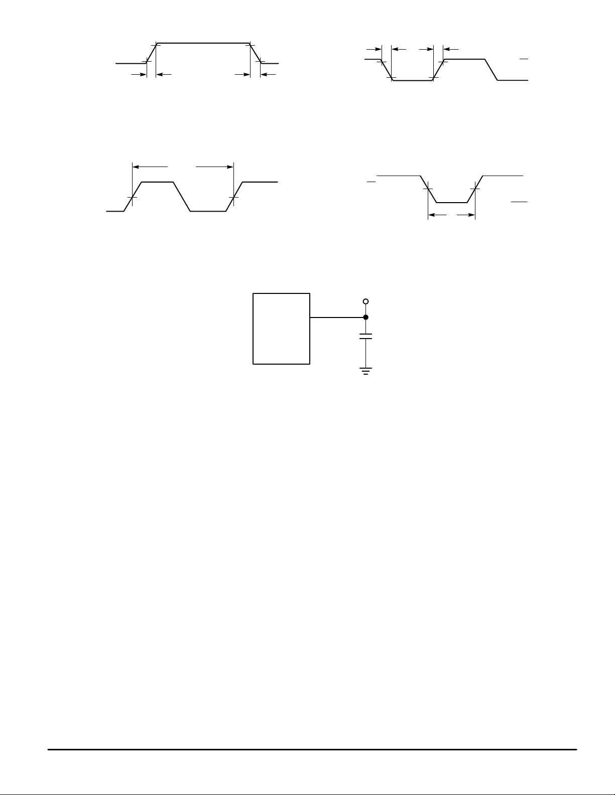
ANY OUTPUT
R
TC
10%
90%
50%
t
f
90%
t
TLH
t
THL
D
in
10%
Figure 4. Figure 5.
1/f
osc
TE
50%
t
w
Figure 6. Figure 7.
TEST POINT
t
r
V
DD
V
SS
V
DD
V
SS
DEVICE
UNDER
TEST
*Includes all probe and fixture capacitance.
OUTPUT
CL*
Figure 8. T est Circuit
MC145026•MC145027•MC145028•SC41343•SC41344MOTOROLA
7

OPERA TING CHARACTERISTICS
MC145026
The encoder serially transmits trinary data as defined by
the state of the A1 – A5 and A6/D6 – A9/D9 input pins. These
pins may be in either of three states (low, high, or open) allowing 19,683 possible codes. The transmit sequence is initiated
by a low level on the TE
MC145026 can continuously transmit as long as TE remains
low (also, the device can transmit two–word sequences by
pulsing TE
be designed to rely upon the first data word transmitted immediately after power–up because this word may be invalid.
Between the two data words, no signal is sent for three data
periods (see Figure 10).
Each transmitted trinary digit is encoded into pulses (see
Figure 11). A logic 0 (low) is encoded as two consecutive
short pulses, a logic 1 (high) as two consecutive long pulses,
and an open (high impedance) as a long pulse followed by a
short pulse. The input state is determined by using a weak
“output” device to try to force each input high then low. If only
a high state results from the two tests, the input is assumed to
be hardwired to VDD. If only a low state is obtained, the input
is assumed to be hardwired to VSS. If both a high and a low
can be forced at an input, an open is assumed and is encoded
as such. The “high” and “low” levels are 70% and 30% of the
supply voltage as shown in the Electrical Characteristics
table. The weak “output” device sinks/sources up to 1 10 µA at
a 5 V supply level, 500 µA at 10 V, and 1 mA at 15 V.
The TE
switch may be used to force the input low. While TE
and the second–word transmission has timed out, the encoder is completely disabled, the oscillator is inhibited, and the
current drain is reduced to quiescent current. When TE
brought low, the oscillator is started and the transmit sequence begins. The inputs are then sequentially selected,
and determinations are made as to the input logic states. This
information is serially transmitted via the D
MC145027
This decoder receives the serial data from the encoder and
outputs the data, if it is valid. The transmitted data, consisting
of two identical words, is examined bit by bit during reception.
The first five trinary digits are assumed to be the address. If
the received address matches the local address, the next four
(data) bits are internally stored, but are not transferred to the
output data latch. As the second encoded word is received,
the address must again match. If a match occurs, the new
data bits are checked against the previously stored data bits.
If the two nibbles of data (four bits each) match, the data is
transferred to the output data latch by VT and remains until
new data replaces it. At the same time, the VT output pin is
brought high and remains high until an error is received or until no input signal is received for four data periods (see Figure
10).
Although the address information may be encoded in trinary, the data information must be either a 1 or 0. A trinary
(open) data line is decoded as a logic 1.
MC145028
This decoder operates in the same manner as the
MC145027 except that nine address lines are used and no
low). However, no MC145026 application should
input has an internal pull–up device so that a simple
input pin. Upon power–up, the
is high
is
pin.
out
data output is available. The VT output is used to indicate that
a valid address has been received. For transmission security ,
two identical transmitted words must be consecutively received before a VT output signal is issued.
The MC145028 allows 19,683 addresses when trinary levels are used. 512 addresses are possible when binary levels
are used.
PIN DESCRIPTIONS
MC145026 ENCODER
A1 – A5, A6/D6 – A9/D9
Address, Address/Data Inputs (Pins 1 – 7, 9, and 10)
These address/data inputs are encoded and the data is
sent serially from the encoder via the D
RS, CTC, R
(Pins 11, 12, and 13)
These pins are part of the oscillator section of the encoder
(see Figure 9).
If an external signal source is used instead of the internal
oscillator, it should be connected to the RS input and the R
and CTC pins should be left open.
TE
Transmit Enable (Pin 14)
This active–low transmit enable input initiates transmission
when forced low. An internal pull–up device keeps this input
normally high. The pull–up current is specified in the Electrical Characteristics table.
D
out
Data Out (Pin 15)
This is the output of the encoder that serially presents the
encoded data word.
VSS
Negative Power Supply (Pin 8)
The most–negative supply potential. This pin is usually
ground.
V
DD
Positive Power Supply (Pin 16)
The most–positive power supply pin.
MC145027 AND MC145028 DECODERS
A1 – A5, A1 – A9
Address Inputs (Pins 1 – 5) — MC145027,
Address Inputs (Pins 1 – 5, 15, 14, 13, 12) — MC145028
These are the local address inputs. The states of these
pins must match the appropriate encoder inputs for the VT pin
to go high. The local address may be encoded with trinary or
binary data.
D6 – D9
Data Outputs (Pins 15, 14, 13, 12) — MC145027 Only
These outputs present the binary information that is on
encoder inputs A6/D6 through A9/D9. Only binary data is
acknowledged; a trinary open at the MC145026 encoder is
decoded as a high level (logic 1).
D
in
Data In (Pin 9)
This pin is the serial data input to the decoder. The input
voltage must be at CMOS logic levels. The signal source driving this pin must be dc coupled.
TC
out
pin.
TC
MC145026•MC145027•MC145028•SC41343•SC41344 MOTOROLA
8

R1, C
1
Resistor 1, Capacitor 1 (Pins 6, 7)
As shown in Figures 2 and 3, these pins accept a resistor
and capacitor that are used to determine whether a narrow
pulse or wide pulse has been received. The time constant
R1 x C1 should be set to 1.72 encoder clock periods:
R1 C1 = 3.95 RTC C
R2/C
2
Resistor 2/Capacitor 2 (Pin 10)
As shown in Figures 2 and 3, this pin accepts a resistor and
capacitor that are used to detect both the end of a received
word and the end of a transmission. The time constant R2 x
C2 should be 33.5 encoder clock periods (four data periods
per Figure 11): R2 C2 = 77 RTC CTC. This time constant is
used to determine whether the Din pin has remained low for
four data periods (end of transmission). A separate on–chip
comparator looks at the voltage–equivalent two data periods
(0.4 R2 C2) to detect the dead time between received words
within a transmission.
TC
VT
Valid Transmission Output (Pin 11)
This valid transmission output goes high after the second
word of an encoding sequence when the following conditions
are satisfied:
1.the received addresses of both words match the local decoder address, and
2.the received data bits of both words match.
VT remains high until either a mismatch is received or no
input signal is received for four data periods.
V
SS
Negative Power Supply (Pin 8)
The most–negative supply potential. This pin is usually
ground.
V
DD
Positive Power Supply (Pin 16)
The most–positive power supply pin.
MC145026•MC145027•MC145028•SC41343•SC41344MOTOROLA
9
11 12 13
INTERNAL
ENABLE
This oscillator operates at a frequency determined by the
external RC network; i.e.,
R
S
C
TC
R
TC
TE
ENCODER
OSCILLA TOR
(PIN 12)
D
out
(PIN 15)
f ≈
1
2.3 RTC CTC′
for 1 kHz ≤ f ≤ 400 kHz
where: CTC′ = CTC + C
RS ≈ 2 R
RS ≥ 20 k
TC
RTC ≥ 10 k
400 pF < CTC < 15 µF
PW
min
2
4
6
(Hz)
The value for RS should be chosen to be ≥ 2 times RTC. This range ensures
that current through RS is insignificant compared to current through RTC. The
upper limit for RS must ensure that RS x 5 pF (input capacitance) is small compared to RTC x CTC.
layout
+ 12 pF
For frequencies outside the indicated range, the formula is less accurate.
The minimum recommended oscillation frequency of this circuit is 1 kHz. Susceptibility to externally induced noise signals may occur for frequencies below
1 kHz and/or when resistors utilized are greater than 1 MΩ.
Figure 9. Encoder Oscillator Information
ENCODER
16182022242628308082848688
1ST
DIGIT
HIGH
OPEN LOW
9TH
DIGIT
2 WORD TRANSMISSION
CONTINUOUS TRANSMISSION
90
114
116
118
120
122
178
180
182
184
1ST
DIGIT
9TH
DIGIT
2ND WORD1ST WORD
ENCODING SEQUENCE
DECODER
1.1 (R2C2)
VT
(PIN 11)
DATA OUTPUTS
Figure 10. Timing Diagram
MC145026•MC145027•MC145028•SC41343•SC41344 MOTOROLA
10

D
out
(PIN 15)
ENCODER
OSCILLA TOR
(PIN 12)
ENCODED
“ONE”
ENCODED
“ZERO”
ENCODED
“OPEN”
DATA PERIOD
Figure 11. Encoder Data Waveforms
500
400
300
max
f (kHz)
(REF. TO ENCODER CLOCK)
200
100
C
(pF) ON PINS 1 – 5 (MC145027); PINS 1 – 5 AND 12 – 15 (MC145028)
layout
Figure 12. f
VDD = 15 V
VDD = 10 V
VDD = 5 V
10 20 30 40 50
max
vs C
— Decoders Only
layout
MC145026•MC145027•MC145028•SC41343•SC41344MOTOROLA
11

NO
HAS
THE TRANSMISSION
BEGUN?
YES
DOES
THE 5–BIT
ADDRESS MATCH
THE ADDRESS
PINS?
YES
STORE
THE
4–BIT
DATA
DOES
THIS DATA
MATCH THE PREVIOUSLY
STORED
DATA?
YES
IS THIS
AT LEAST THE
2ND CONSECUTIVE
MATCH SINCE VT
DISABLE?
YES
LATCH DATA
ONTO OUTPUT
PINS AND
ACTIVATE VT
NO
NO
NO
DISABLE VT
ON THE 1ST
ADDRESS MISMATCH
DISABLE VT
ON THE 1ST
DATA MISMA TCH
NO
HAVE
4–BIT TIMES
PASSED?
NO
HAS
A NEW
TRANSMISSION
BEGUN?
YES
YES
DISABLE
VT
Figure 13. MC145027 Flowchart
MC145026•MC145027•MC145028•SC41343•SC41344 MOTOROLA
12

NO
HAS
THE TRANSMISSION
BEGUN?
YES
DOES
THE ADDRESS
MATCH THE
ADDRESS
PINS?
YES
IS
THIS AT LEAST
THE 2ND CONSECUTIVE
MATCH SINCE VT
DISABLE?
YES
ACTIVATE VT
HAVE
4–BIT TIMES
PASSED?
NO
NO
YES
DISABLE VT ON THE 1ST
ADDRESS MISMATCH
AND IGNORE THE REST
OF THIS WORD
DISABLE VT
NO
NO
HAS A
NEW TRANSMISSION
BEGUN?
YES
Figure 14. MC145028 Flowchart
MC145026•MC145027•MC145028•SC41343•SC41344MOTOROLA
13
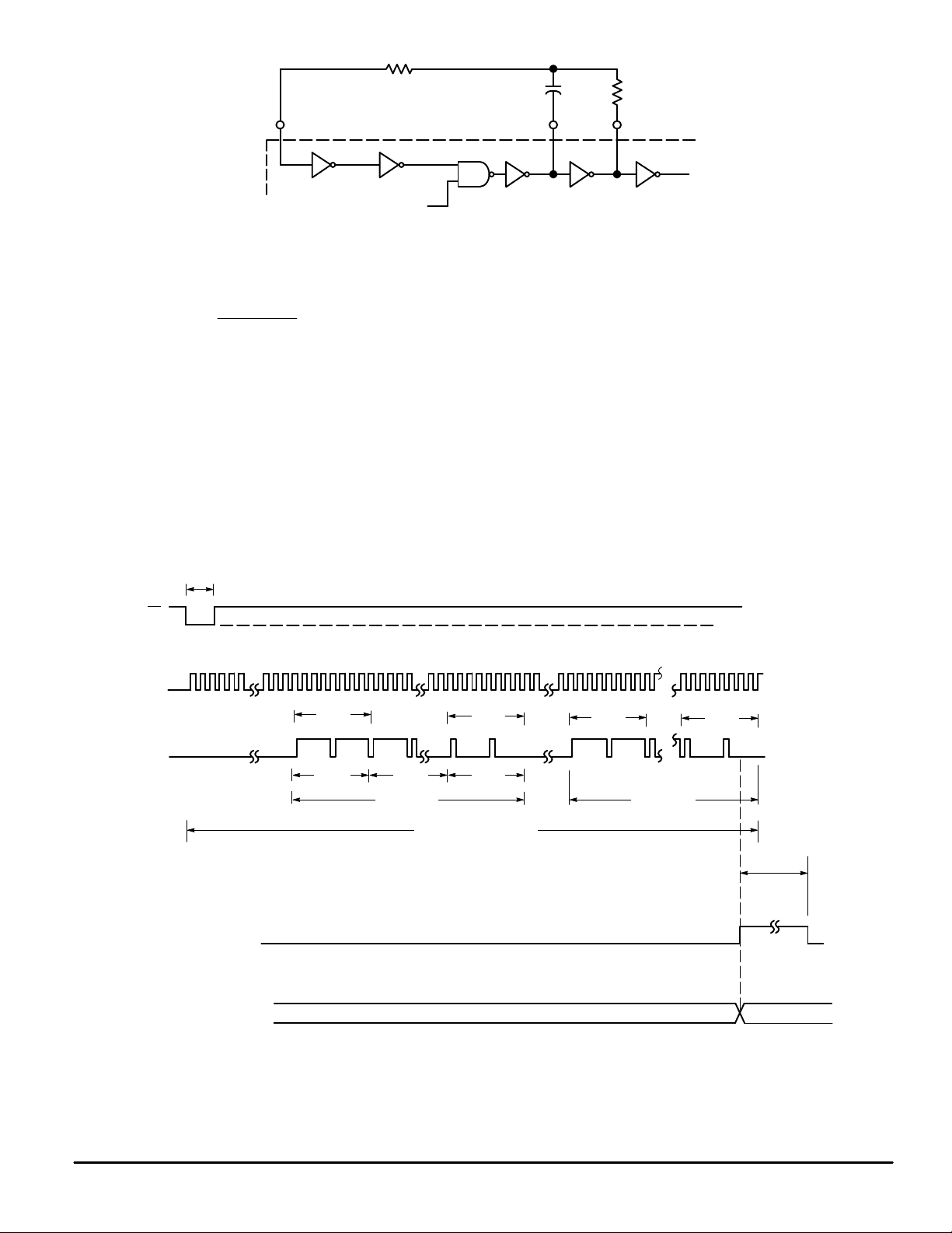
MC145027 AND MC145028 TIMING
To verify the MC145027 or MC145028 timing, check the
waveforms on C1 (Pin 7) and R2/C2 (Pin 10) as compared to
the incoming data waveform on Din (Pin 9).
The R–C decay seen on C1 discharges down to 1/3 V
before being reset to VDD. This point of reset (labelled “DOS”
in Figure 15) is the point in time where the decision is made
whether the data seen on Din is a 1 or 0. DOS should not be
too close to the Din data edges or intermittent operation may
occur.
The other timing to be checked on the MC145027 and
MC145028 is on R2/C2 (see Figure 16). The R–C decay is
continually reset to VDD as data is being transmitted. Only
between words and after the end–of–transmission (EOT)
does R2/C2 decay significantly from VDD. R2/C2 can be used
to identify the internal end–of–word (EOW) timing edge which
is generated when R2/C2 decays to 2/3 VDD. The internal
EOT timing edge occurs when R2/C2 decays to 1/3 VDD.
When the waveform is being observed, the R–C decay
should go down between the 2/3 and 1/3 VDD levels, but not
too close to either level before data transmission on Din resumes.
Verification of the timing described above should ensure a
good match between the MC145026 transmitter and the
MC145027 and MC145028 receivers.
DD
D
in
C1
R2/C2
V
DD
0 V
V
DD
2/3
1/3
0 V
DOS DOS
Figure 15. R–C Decay on Pin 7 (C1)
V
DD
2/3
1/3
0 V
Figure 16. R–C Decay on Pin 10 (R2/C2)
EOW
EOT
MC145026•MC145027•MC145028•SC41343•SC41344 MOTOROLA
14

5
TRINARY
ADDRESSES
4–BIT
BINARY
DATA
F
6
7
V
DD
16
MC145027
OR
SC41343
8
15
14
13
12
11
V
DD
A1
A2
1
A3
2
3
A4
4
A5
5
D6
D7
D8
D9
VT
5
TRINARY
ADDRESSES
V
V
DD
A1
A2
A3
A4
A5
D6
D7
D8
D9
1
2
3
4
5
6
7
9
10
TE
14 16
MC145026
8
DD
15 D
13
12
11
0.1
µ
F
out
R
TC
C
TC
R
S
R2
0.1 µ
Din9
R1
C
1
C
2
10
f
=
osc
R1C1 = 3.95 RTCC
R2C2 = 77 RTCC
1
2.3 RTCCTC′
CTC′ = CTC + C
TC
TC
Example R/C Values (All Resistors and Capacitors are ±5%)
(CTC′ = CTC + 20 pF)
f
(kHz) R
osc
362
181
88.7
42.6
21.5
8.53
1.71
+ 12 pF
100 pF ≤ CTC ≤ 15 µF
RTC ≥ 10 kΩ; RS ≈ 2 R
R1 ≥ 10 kΩ
C1 ≥ 400 pF
R2 ≥ 100 kΩ
C2 ≥ 700 pF
TC
10 k
10 k
10 k
10 k
10 k
10 k
50 k
layout
C
TC′
120 pF
240 pF
490 pF
1020 pF
2020 pF
5100 pF
5100 pF
Figure 17. T ypical Application
TC
R
S
20 k
20 k
20 k
20 k
20 k
20 k
100 k
R
10 k
10 k
10 k
10 k
10 k
10 k
50 k
REPEAT OF ABOVE
REPEAT OF ABOVE
1
C
1
470 pF
910 pF
2000 pF
3900 pF
8200 pF
0.02 µF
0.02 µF
R
2
100 k
100 k
100 k
100 k
100 k
200 k
200 k
C
2
910 pF
1800 pF
3900 pF
7500 pF
0.015 µF
0.02 µF
0.1 µF
MC145026•MC145027•MC145028•SC41343•SC41344MOTOROLA
15

APPLICATIONS INFORMATION
INFRARED TRANSMITTER
In Figure 18, the MC145026 encoder is set to run at an oscillator frequency of about 4 to 9 kHz. Thus, the time required
for a complete two–word encoding sequence is about 20 to
40 ms. The data output from the encoder gates an RC oscillator running at 50 kHz; the oscillator shown starts rapidly
enough to be used in this application. When the “send” button
is not depressed, both the MC145026 and oscillator are in a
low–power standby state. The RC oscillator has to be
trimmed for 50 kHz and has some drawbacks for frequency
stability . A superior system uses a ceramic resonator oscillator running at 400 kHz. This oscillator feeds a divider as
shown in Figure 19. The unused inputs of the MC14011UB
must be grounded.
The MLED81 IRED is driven with the 50 kHz square wave
at about 200 to 300 mA to generate the carrier. If desired, two
IREDs wired in series can be used (see Application Note
AN1016 for more information). The bipolar IRED switch,
shown in Figure 18, offers two advantages over a FET. First,
a logic FET has too much gate capacitance for the
MC14011UB to drive without waveform distortion. Second,
the bipolar drive permits lower supply voltages, which are an
advantage in portable battery–powered applications.
The configuration shown in Figure 18 operates over a
supply range of 4.5 to 18 V. A low–voltage system which
operates down to 2.5 V could be realized if the oscillator section of a MC74HC4060 is used in place of the MC14011UB.
The data output of the MC145026 is inverted and fed to the
RESET pin of the MC74HC4060. Alternately, the
MC74HCU04 could be used for the oscillator.
Information on the MC14011UB is in book number
DL131/D. The MC74HCU04 and MC74HC4060 are found in
book number DL129/D.
INFRARED RECEIVER
The receiver in Figure 20 couples an IR–sensitive diode to
input preamp A1, followed by band–pass amplifier A2 with a
gain of about 10. Limiting stage A3 follows, with an output of
about 800 mV p–p. The limited 50 kHz burst is detected by
comparator A4 that passes only positive pulses, and peak–
detected and filtered by a diode/RC network to extract the
data envelope from the burst. Comparator A5 boosts the signal to logic levels compatible with the MC145027/28 data
input. The Din pin of these decoders is a standard CMOS
not
high–impedance input which must
Therefore, direct coupling from A5 to the decoder input is
utilized.
Shielding should be used on at least A1 and A2, with good
ground and high–sensitivity circuit layout techniques applied.
For operation with supplies higher than + 5 V, limiter A4’s
positive output swing needs to be limited to 3 to 5 V. This is
accomplished via adding a zener diode in the negative feedback path, thus avoiding excessive system noise. The biasing resistor stack should be adjusted such that V3 is 1.25 to
1.5 V.
This system works up to a range of about 10 meters. The
gains of the system may be adjusted to suit the individual
design needs. The 100
2N5088 and the 1 k
different gain is required. In general, more gain does not necessarily result in increased range. This is due to noise floor
limitations. The designer should increase transmitter power
and/or increase receiver aperature with Fresnal lensing to
greatly improve range. See Application Note AN1016 for
additional information.
Information on the MC34074 is in data book DL128/D.
TRINARY SWITCH MANUFACTURERS
Midland Ross–Electronic Connector Div.
Greyhill
Augat/Alcoswitch
Aries Electronics
The above companies may not have the switches in a DIP.
For more information, call them or consult
gineers Master Catalog
Ω resistor in the emitter of the first
Ω resistor feeding A2 may be altered if
or the
Gold Book. Ask for SPDT with
be allowed to float.
eem Electronic En-
center OFF.
Alternative: An SPST can be placed in series between a
SPDT and the Encoder or Decoder to achieve trinary action.
Motorola cannot recommend one supplier over another
and in no way suggests that this is a complete listing of trinary
switch manufacturers.
MC145026•MC145027•MC145028•SC41343•SC41344 MOTOROLA
16

V+
SELECT FOR
200 mA TO 300 mA
SEND
9
SWITCHES
TE
MC145026
R
S
220 k
MC14011UB
MC14011UB
D
out
C
TC
Ω
R
TC
1000 pF
100 kΩ FOR APPROX. 4 kHz
47 k
Ω
FOR APPROX. 9 kHz
220 k
Ω
10 k
Ω
0.01 µF
ADJUST/SELECT FOR
f = 50 kHz (APPROX. 100 k
Figure 18. IRED Transmitter Using RC Oscillator to Generate Carrier Frequency
MLED81
USE OF 2 MLED81s
IS OPTIONAL
MPSA13
OR
MPSW13
Ω
)
470 pF
V+
1M
X1
MC14011UB
Ω
X1 = 400 kHz CERAMIC RESONAT OR
PANASONIC EFD–A400K04B
OR EQUIVALENT
470 pF
MC14024
CLK
RESET
V+
D
out
FROM MC145026
MC14011UB
Figure 19. Using a Ceramic Resonator to Generate Carrier Frequency
Q3
50 kHZ TO
DRIVER
TRANSISTOR
MC145026•MC145027•MC145028•SC41343•SC41344MOTOROLA
17

10
OPTICAL
FILTER
100 k
µ
F
1N914
1N914
+5 V
Ω
10 k
22 k
Ω
Ω
10 k
2N5088
10 k
100
1 µ
A1
10 µ
0.01 µ
F
F
1 k
Ω
2N5086
Ω
Ω
F
1 M
Ω
6.8 k
Ω
2N5088
2.2 k
Ω
1 mH — TOKO TYPE 7P A OR 10PA
OR EQUIVALENT
0.01 µ
F
Ω
Ω
V1
1/4 MC34074
–
A2
+
0.01 µF4.7 k
1 M
Ω
V1
+5 V
–
A3
+
1/4 MC34074
1000 pF
C1
D
in
V
DD
10 k
Ω
V2
1/4 MC34074
390 kΩ FOR APPROX. 4 kHz
180 k
Ω
FOR APPROX. 9 kHz
R1 R2/C2
MC145027/28
V
SS
9 FOR MC145027
5 FOR MC145028
ADDRESS
SWITCHES
0.01 µ
4
1N914
F
1 k
750 k
360 k
DATA OUT
MC145027 ONLY
Ω
1000 pF 47 k
Ω
FOR APPROX. 4 kHz
Ω
FOR APPROX. 9 kHz
Ω
10 µF
22 k
10 µF
Ω
V3
+5 V
10 µF
+
A5
–
1/4 MC34074
4.7 k
Ω
390
Ω
2.2 k
Ω
2.7 k
Ω
V2
V1
V3
≈
2.7 V
≈
2.5 V
≈
1.3 V
+
A4
–
VT
Figure 20. Infrared Receiver
MC145026•MC145027•MC145028•SC41343•SC41344 MOTOROLA
18

P ACKAGE DIMENSIONS
PLASTIC DIP (DUAL IN–LINE PACKAGE)
–A–
916
B
18
F
C
S
–T–
H
G
D
16 PL
0.25 (0.010) T
K
M
A
SOG (SMALL OUTLINE GULL–WING) PACKAGE
–A–
16 9
–B–
18
G
K
C
–T–
SEATING
PLANE
D
16 PL
0.25 (0.010) A
M
S
B
T
S
SEATING
PLANE
M
8 PLP
0.25 (0.010) B
P SUFFIX
CASE 648–08
L
J
D SUFFIX
CASE 751B–05
M
R
X 45
M
NOTES:
1. DIMENSIONING AND TOLERANCING PER ANSI
Y14.5M, 1982.
2. CONTROLLING DIMENSION: INCH.
3. DIMENSION L TO CENTER OF LEADS WHEN
FORMED PARALLEL.
4. DIMENSION B DOES NOT INCLUDE MOLD FLASH.
5. ROUNDED CORNERS OPTIONAL.
DIM MIN MAX MIN MAX
A 0.740 0.770 18.80 19.55
B 0.250 0.270 6.35 6.85
C 0.145 0.175 3.69 4.44
D 0.015 0.021 0.39 0.53
F 0.040 0.70 1.02 1.77
G 0.100 BSC 2.54 BSC
M
S
_
J
H 0.050 BSC 1.27 BSC
J 0.008 0.015 0.21 0.38
K 0.110 0.130 2.80 3.30
L 0.295 0.305 7.50 7.74
M 0 10 0 10
S 0.020 0.040 0.51 1.01
NOTES:
1. DIMENSIONING AND TOLERANCING PER ANSI
Y14.5M, 1982.
2. CONTROLLING DIMENSION: MILLIMETER.
3. DIMENSIONS A AND B DO NOT INCLUDE
MOLD PROTRUSION.
4. MAXIMUM MOLD PROTRUSION 0.15 (0.006)
PER SIDE.
5. DIMENSION D DOES NOT INCLUDE DAMBAR
PROTRUSION. ALLOWABLE DAMBAR
PROTRUSION SHALL BE 0.127 (0.005) TOTAL
IN EXCESS OF THE D DIMENSION AT
MAXIMUM MATERIAL CONDITION.
DIM MIN MAX MIN MAX
F
A 9.80 10.00 0.386 0.393
B 3.80 4.00 0.150 0.157
C 1.35 1.75 0.054 0.068
D 0.35 0.49 0.014 0.019
F 0.40 1.25 0.016 0.049
G 1.27 BSC 0.050 BSC
J 0.19 0.25 0.008 0.009
K 0.10 0.25 0.004 0.009
M 0 7 0 7
P 5.80 6.20 0.229 0.244
R 0.25 0.50 0.010 0.019
MILLIMETERSINCHES
____
INCHESMILLIMETERS
____
MC145026•MC145027•MC145028•SC41343•SC41344MOTOROLA
19

–A–
16 9
D16X
M
0.010 (0.25) B
A
T
G14X
SOG (SMALL OUTLINE GULL–WING) PACKAGE
DW SUFFIX
CASE 751G–02
–B– P8X
M
M
0.010 (0.25)
81
B
J
S
S
F
R
X 45
_
C
K
–T–
SEATING
PLANE
M
NOTES:
1. DIMENSIONING AND TOLERANCING PER ANSI
Y14.5M, 1982.
2. CONTROLLING DIMENSION: MILLIMETER.
3. DIMENSIONS A AND B DO NOT INCLUDE MOLD
PROTRUSION.
4. MAXIMUM MOLD PROTRUSION 0.15 (0.006) PER
SIDE.
5. DIMENSION D DOES NOT INCLUDE DAMBAR
PROTRUSION. ALLOWABLE DAMBAR
PROTRUSION SHALL BE 0.13 (0.005) TOTAL IN
EXCESS OF D DIMENSION AT MAXIMUM
MATERIAL CONDITION.
DIM MIN MAX MIN MAX
A 10.15 10.45 0.400 0.411
B 7.40 7.60 0.292 0.299
C 2.35 2.65 0.093 0.104
D 0.35 0.49 0.014 0.019
F 0.50 0.90 0.020 0.035
G 1.27 BSC 0.050 BSC
J 0.25 0.32 0.010 0.012
K 0.10 0.25 0.004 0.009
M 0 7 0 7
____
P 10.05 10.55 0.395 0.415
R 0.25 0.75 0.010 0.029
INCHESMILLIMETERS
Motorola reserves the right to make changes without further notice to any products herein. Motorola makes no warranty , representation or guarantee regarding
the suitability of its products for any particular purpose, nor does Motorola assume any liability arising out of the application or use of any product or circuit, and
specifically disclaims any and all liability, including without limitation consequential or incidental damages. “T ypical” parameters which may be provided in Motorola
data sheets and/or specifications can and do vary in different applications and actual performance may vary over time. All operating parameters, including “Typicals”
must be validated for each customer application by customer’s technical experts. Motorola does not convey any license under its patent rights nor the rights of
others. Motorola products are not designed, intended, or authorized for use as components in systems intended for surgical implant into the body, or other
applications intended to support or sustain life, or for any other application in which the failure of the Motorola product could create a situation where personal injury
or death may occur. Should Buyer purchase or use Motorola products for any such unintended or unauthorized application, Buyer shall indemnify and hold Motorola
and its officers, employees, subsidiaries, affiliates, and distributors harmless against all claims, costs, damages, and expenses, and reasonable attorney fees
arising out of, directly or indirectly, any claim of personal injury or death associated with such unintended or unauthorized use, even if such claim alleges that
Motorola was negligent regarding the design or manufacture of the part. Motorola and are registered trademarks of Motorola, Inc. Motorola, Inc. is an Equal
Opportunity/Affirmative Action Employer.
How to reach us:
Mfax is a trademark of Motorola, Inc.
USA/EUROPE /Locations Not Listed: Motorola Literature Distribution; JAPAN: Nippon Motorola Ltd.; SPD, Strategic Planning Office; 4-32-1,
P.O. Bo x 5405, Denver, Colorado, 80217. 1-303-675-2140 or 1-800-441-2447 Nishi-Gotanda; Shinagawa-ku, T okyo 141, Japan. 81-3-5487-8488
Mfax: RMFAX0@email.sps.mot.com – TOUCHTONE 1-602-244-6609 ASIA/PACIFIC: Motorola Semiconductors H.K. Ltd.; 8B Tai Ping Industrial Park,
Motorola Fax Back System – US & Canada ONLY 1-800-774-1848 51 Ting Kok Road, Tai Po, N.T., Hong Kong. 852-26629298
– http://sps.motorola.com/mfax /
HOME PAGE: http://motorola.com/sps / CUSTOMER FOCUS CENTER: 1-800-521-6274
MC145026•MC145027•MC145028•SC41343•SC41344 MOTOROLA
◊
MC145026/D
20
 Loading...