Motorola MC141627FT Datasheet
SEMICONDUCTOR TECHNICAL DATA
Product Preview
Order this document
by MC141627/D
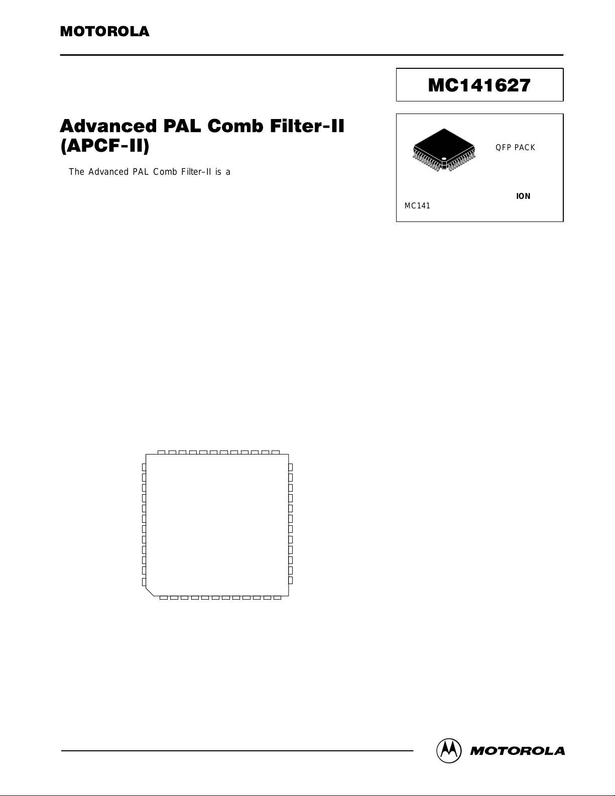
The Advanced PAL Comb Filter–II is a video signal processor for VCRs,
LDPs, and TVs. It separates the Luminance Y and Chrominance C signal from
the NTSC/PAL composite signal by using digital signal processing techniques
which minimize dot–crawl and cross–color. The built–in 4xFSC PLL circuit
allows a subcarrier signal input, which generates 4xFSC clock for video signal
processing. This filter allows a video signal input of an extended frequency
bandwidth by using a 4xFSC clock. The built–in vertical enhancer circuit
reduces noise and dot crawl on the Luminance Y signal. The built–in A/D and
D/A converters allow easy connection to analog video circuits.
• Built–In High Speed 8–Bit A/D Converter
• Four Line Memories (4540 Bytes)
• Advanced Comb–II Process
• Built–In Vertical Enhancer
• Vertical Dot Reduction Process
• Two Built–In High Speed 8–Bit D/A Converters
• Built–In 4xFSC PLL Circuit
• Built–In Clamp Circuit
• Digital Interface Mode
• On–Chip Reference Voltage for A/D Converter
PIN ASSIGNMENT
FT SUFFIX
QFP PACKAGE
CASE 898
1
48
ORDERING INFORMATION
MC141627FT Quad Flat Package (QFP)
D5D6D7C0C1
D4
36
D3
37
D2
D1
D0
BYPASS
VH
GND(D)
V
CC(D)
FSC
N/M
PAL/NTSC
Comb/BPF
This document contains information on a product under development. Motorola reserves the right to change or discontinue this product without notice.
REV 0.1
8/96
48
1
CC
PCO
BIAS
FILIN
OV
NC = NO CONNECTION
C2
out
Y
CC(DA)
V
GND(DA)
C3
C4C5C6
out
C
REF(DA)
bias
I
GND(AD)
C7
25
24
13
12
CC(AD)
V
TE1
TE0
MODE1
MODE0
CLK(AD)
GND(D)
NC
CLC
CL
out
V
in
RBT
RTP
Motorola, Inc. 1996
MOTOROLA
MC141627
1
NC (D3)
NC (D2)
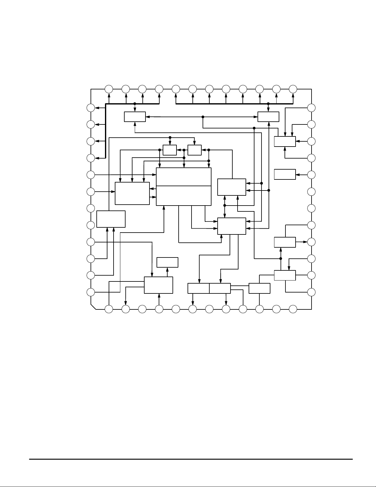
BLOCK DIAGRAM
NOISE LEVEL 2 (D5)
NOISE LEVEL 3 (D6)
NOISE LEVEL 4 (D7)
WHITE LEVEL 1 (C0)
WHITE LEVEL 2 (C1)
NOISE LEVEL 1 (D4)
36 35 34 33 32 31 30 29 28 27 26 25
37
PORT PORT
38
WHITE LEVEL 3 (C2)
WHITE LEVEL 4 (C3)
BLACK LEVEL 1 (C4)
BLACK LEVEL 2 (C5)
BLACK LEVEL 3 (C6)
BLACK LEVEL 4 (C7)
24
23
TE1
TE0
NC (D1)
NC (D0)
BYPASS
VH
GND(D)
V
CC(D)
FSC
N/M
PAL/NTSC
COMB/BPF
39
40
41
42
43
44
45
46
47
48
MODE
1H/2H
PROCESSING
ADAPTIVE
VERTICAL
ENHANCER
MEMORY
MODE
1 2 3 4 5 6 7 8 9 10 11 12
CC
PCO
OV
BIAS
VERTICAL DOT
PROCESSING
CLKBUF
CLOCK
GEN
FILIN
1H/2H
ACF–II
GND(DA)
Y
out
DACDAC
CC(DA)
V
CONTROL
LOGIC
CONTROL
LOGIC
out
C
I
bias
REF(DA)
bias
I
CLKBUF
CLAMP
GND(AD)
ADC
CC(AD)
V
22
21
20
19
18
17
16
15
14
13
MODE1
MODE0
CLK(AD)
GND(D)
NC
CLC
CL
out
V
in
RBT
RTP
MC141627
2
*( ): Digital input mode
MOTOROLA
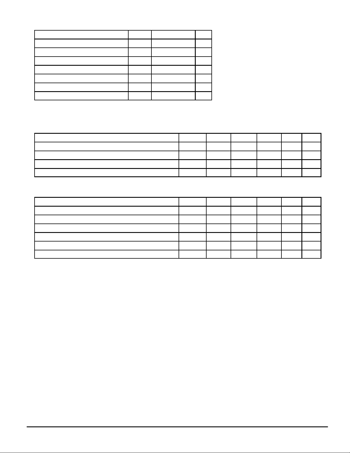
ABSOLUTE MAXIMUM RATINGS*
Characteristic Symbol Value Unit
DC Supply Voltage (Referenced to GND) V
DC Input Voltage (Referenced to GND) V
DC Output Voltage (Referenced to GND) V
DC Input Current (per Pin) I
DC Output Current (per Pin) I
Power Dissipation P
Storage Temperature T
*Maximum Ratings are those values beyond which damage to the device may occur . Func-
tional operation should be restricted to the limits in the Electrical Characteristics tables or
Pin Descriptions section.
CC
in
out
in
out
D
stg
– 0.5 to + 7.0 V
– 1.5 to VCC + 1.5 V
– 0.5 to VCC + 0.5 V
± 20 mA
± 25 mA
750 mW
– 65 to + 150 °C
This device contains protection circuitry to
guard against damage due to high static
voltages or electric fields. However, precautions must be taken to avoid applications of any
voltage higher than maximum rated voltages to
this high–impedance circuit. For proper operation, Vin and V
range GND ≤ (Vin or V
Unused inputs must always be tied to an
appropriate logic voltage level (e.g., either
GND or VCC). Unused outputs must be left
open.
should be constrained to the
out
) ≤ VCC.
out
GENERAL ELECTRICAL CHARACTERISTICS (V
Characteristic Symbol Min Typ Max Unit Notes
Supply Voltage VCC* 4.75 5.0 5.25 V
Operating Supply Current (at Normal Mode) I
Operating Power Dissipation (at Normal Mode) P
Ambient Operating Temperature T
*V
CC(AD)
, V
CC(DA)
, V
CC(D)
voltage.
CLOCK INPUT ELECTRICAL CHARACTERISTICS (V
Characteristic
Subcarrier Input Frequency f
Clock Frequency CLK — 17.734475 — MHz 2
FSC Clock Input Level V
High Level Input Voltage CLK(AD) V
Low Level Input Voltage CLK(AD) V
Clock Duty Cycle CLK/CLK(AD) Dty 45 50 55 % 4
NOTES:
1. Color subcarrier input [FSC = (455/2) fh] locked on the burst signal of the input video signal. AC coupling input by external capacitor.
2. The internal circuit operates by 4 times clock using FSC pin input at normal (FSC) mode.
The internal circuit operates by FSC pin input clock at expected normal (FSC) mode.
3. Sine wave input.
4. CLK(AD) is available only during digital input comb filter mode.
= 5.0 V, TA = 25°C ± 3°C, Unless Otherwise Noted)
CC
CC
D
A
= 5.0 V, TA = 25°C ± 3°C, Unless Otherwise Noted)
CC
Symbol Min Typ Max Unit Notes
c
fc
ICH
ICL
— 65 100 mA
— 325 525 mW
– 20 — 75 °C
— 4.43618 — MHz 1
1 — — V p–p 3
3.5 — — V 4
— — 1.1 V 4
MOTOROLA
MC141627
3
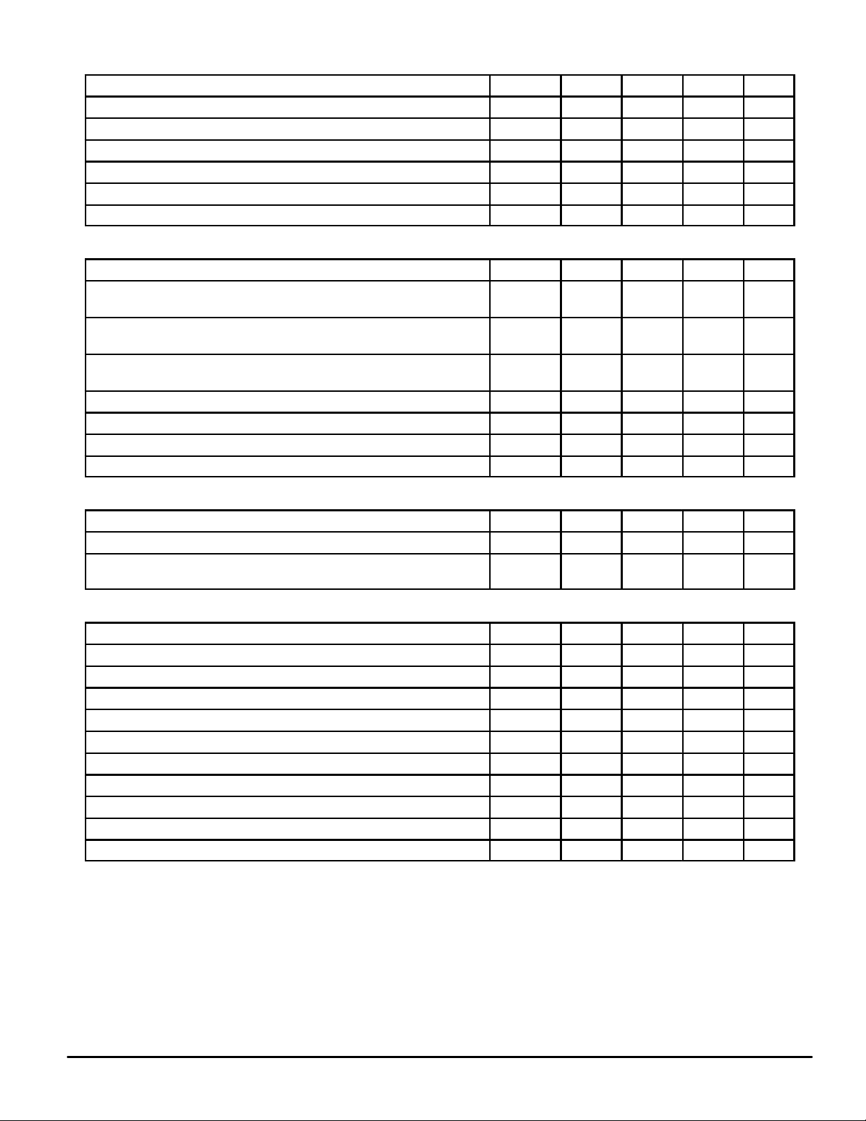
ADC ELECTRICAL CHARACTERISTICS (V
Characteristic
Resolution — — — 8 Bits
Integral Nonlinearity INL — ± 1.0 ± 1.5 LSB
Differential Nonlinearity DNL — ± 0.5 ± 1.0 LSB
Top Reference Level V
Bottom Reference Level V
Maximum Analog Input Range During Self Reference V
= 5.0 V, TA = 25°C ± 3°C)
CC
Symbol Min Typ Max Unit
TPS
BTS
ins
2.4 2.5 2.6 V
0.4 0.5 0.6 V
1.9 2.0 2.1 V p–p
DIGITAL ELECTRICAL CHARACTERISTICS (V
Characteristic
High Level Input Voltage MODE0, MODE1, TE0, TE1, BK,
Low Level Input Voltage MODE0, MODE1, TE0, TE1, BK, VH,
Input Leakage Current MODE0, MODE1, TE0, TE1, BK, VH,
[Vin = V
Data Setup Time (at Digital Input Comb Filter Mode) D0 – D7 t
Data Hold Time (at Digital Input Comb Filter Mode) D0 – D7 t
Data Input Rise Time (at Digital Input Comb Filter Mode) D0 – D7 t
Data Input Fall Time (at Digital Input Comb Filter Mode) D0 – D7 t
FILTERING CHARACTERISTICS (V
Y/C Separation — 40 — — dB
Band–Pass Filter Bandwidth (at – 3 dB) [( ): NTSC] — — ± 0.90
or GND(D)] C0 – C7, D0 – D7
CC(D)
= 5.0 V, TA = 25°C ± 3°C)
CC
Characteristic
DAC ELECTRICAL CHARACTERISTICS (V
Characteristic
Resolution — — — 8 Bits
Integral Nonlinearity INL — — ± 1 LSB
Differential Nonlinearity DNL — — ± 0.5 LSB
Analog Output Voltage, Y
Analog Output Voltage, C
Full Scale Voltage, Y
Full Scale Voltage, C
Zero Scale Voltage, Y
Zero Scale Voltage, C
Output Impedance Z
out
out
out
out
out
out
= 5.0 V, TA = 25°C ± 3°C)
CC
VH, C0 – C7, D0 – D7
C0 – C7, D0 – D7
= 5.0 V, TA = 25°C ± 3°C)
CC
Symbol Min Typ Max Unit
V
IH
V
IL
I
inl
ds
dh
r
f
Symbol Min Typ Max Unit
Symbol Min Typ Max Unit
V
YO
V
CO
V
YFS
V
CFS
V
YZS
V
CZS
O
3.15 — — V
— — 1.1 V
— — ±10 µA
0 — — ns
20 — — ns
— — 10 ns
— — 10 ns
— MHz
(± 0.75)
1.1 1.2 1.3 V p–p
1.1 1.2 1.3 V p–p
1.3 1.5 1.7 V
1.3 1.5 1.7 V
0.1 0.3 0.5 V
0.1 0.3 0.5 V
— 100 300 Ω
MC141627
4
MOTOROLA
ADC – DAC GENERAL CHARACTERISTICS (V
Characteristic
Voltage Gain — – 4.4 — dB
Output Bandwidth (at – 3 dB at PAL) 6.4 7.3 — MHz
Differential Gain DG — — 5 %
Differential Phase DP — — 5 Deg
Bias Current (at I
= 10 kΩ) I
bias
= 5.0 V, TA = 25°C ± 3°C)
CC
Symbol Min Typ Max Unit
bias
— 135 — µA
CLAMP CIRCUIT CHARACTERISTICS (V
Characteristic
Clamp Mode Output Voltage* V
*Output of CL
BK/VH CHARACTERISTICS (V
Bypass Switching Time, at Normal Mode — 9 — Clock
VH Switching Time, at Normal Mode — 4 — Clock
Comb/BPF Switching Time, at Normal Mode — 16 — Clock
when connecting Vin – CL
out
Characteristic
= 5.0 V, TA = 25°C ± 3°C)
CC
VERTICAL ENHANCER LEVEL CHARACTERISTICS (V
Characteristic
Noise Slice Level, at Normal Mode 0 6 15 Bits
White Enhance Level, at Normal Mode 0 10 15 Bits
Black Enhance Level, at Normal Mode 0 11 15 Bits
GENERAL SIGNAL DELAY (V
PAL B/G/H/I Mode (2299.5 Clock) — 129.66 — µs
NTSC Mode (939.5 Clock) — 65.62 — µs
PAL N Mode (1867.5 Clock) — 130.34 — µs
PAL M Mode (1851.5 Clock) — 129.45 — µs
= 5.0 V, TA = 25°C ± 3°C)
CC
Characteristic
= 5.0 V, TA = 25°C ± 3°C)
CC
.
out
Symbol Min Typ Max Unit
Symbol Min Typ Max Unit
= 5.0 V, TA = 25°C ± 3°C)
CC
Symbol Min Typ Max Unit
Symbol Min Typ Max Unit
clys
— 0.6 — V
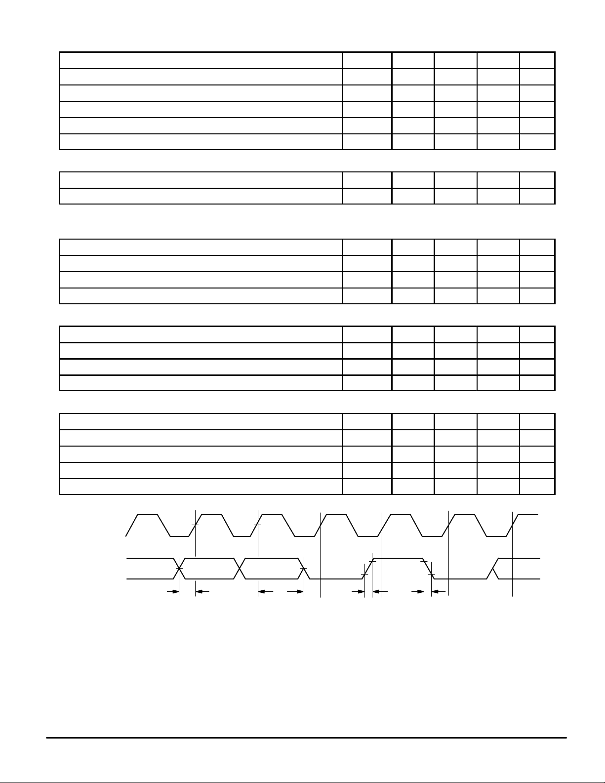
CLOCK
INPUT DATA
(D0 – D7)
t
ds
t
dh
Figure 1. Digital Signal Input Timing Diagram (During Digital Input Comb Filter Mode)
Clamp Circuit Characteristics (VCC = 5.0 V, TA = 25°C ± 3°C)
Clamp Mode Output Voltage, V
V
= (VTP – VBT) (N + 1) / 256 + VBT ± 50 mV
cly
(Non–input when connecting Vin – CL
cly
where N = Clamp Code Input (N < 255)
• If the calculated value of the output voltage, V
cly
> V
clys
, then V
• Clamp Value N is fixed, N = 4.
MOTOROLA
cly
t
r
= V
out
clys
t
f
)
MC141627
5
 Loading...