

Motorola MC141541P Datasheet
SEMICONDUCTOR TECHNICAL DATA
Order this document
by MC141541/D
CMOS
The MC141541 is a high performance HCMOS device designed to interface
with a microcontroller unit to allow colored symbols or characters to be
displayed on a color monitor. The on–chip PLL allows both multi–system
operation and self–generation of system timing. It also minimizes the MCU’s
burden through its built–in 273 bytes display/control RAM. By storing a full
screen of data and control information, this device has the capability to carry out
‘screen–refresh’ without MCU supervision.
Since there is no spacing between characters, special graphics–oriented
characters can be generated by combining two or more character blocks. There
are two different resolutions that users can choose. By changing the number of
dots per horizontal line to 320 (CGA) or 480 (EGA), smaller characters with
higher resolution can be easily achieved.
Special functions such as character bordering or shadowing, multi–level
windows, double height and double width, and programmable vertical length of
character can also be incorporated. Furthermore, neither massive information
update nor extremely high data transmission rate are expected for normal on–
screen display operation, and serial protocols are implemented in lieu of any
parallel formats to achieve minimum pin count.
A special feature, character RAM fonts, is implemented in this MOSD
enhanced version (EMOSD). Users can download their own fonts and display
them at any time once the chip is powered on. There are two ways for users to
build and store fonts. One is a conventional approach to have masked ROM
fonts. A newer approach is to store the fonts in the EPROM accessed by the
MCU and then download them into the EMOSD character RAM. With this new
technique, users have more flexibility in preparing their fonts and the effective
number of fonts is greatly increased.
• Two Selectable Resolutions: 320 (CGA) and 480 (EGA) Dots per Line
• Fully Programmable Character Array of 10 Rows by 24 Columns
• 273 Bytes Direct Mapping Display RAM Architecture
• Internal PLL Generates a Wide–Ranged System Clock
• For High–End Monitor Application, Maximum Horizontal Frequency is
110 kHz (52.8 MHz Dot Clock at 480 Mode)
• Programmable Vertical Height of Character to Meet Multi–Sync
Requirement
• Programmable Vertical and Horizontal Positioning for Display Center
• 120 Characters and Graphic Symbols ROM and Eight Programmable
Character RAM
• 10 x 16 Dot Matrix Character
• Character–by–Character Color Selection
• A Maximum of Four Selectable Colors per Row
• Double Character Height and Double Character Width
• Character Bordering or Shadowing
• Three Fully Programmable Background Windows with Overlapping
Capability
• Provides a Clock Output Synchronous to the Incoming H Sync for External
PWM
• M_BUS (IIC) Interface with Address $7A
• Single Positive 5 V Supply
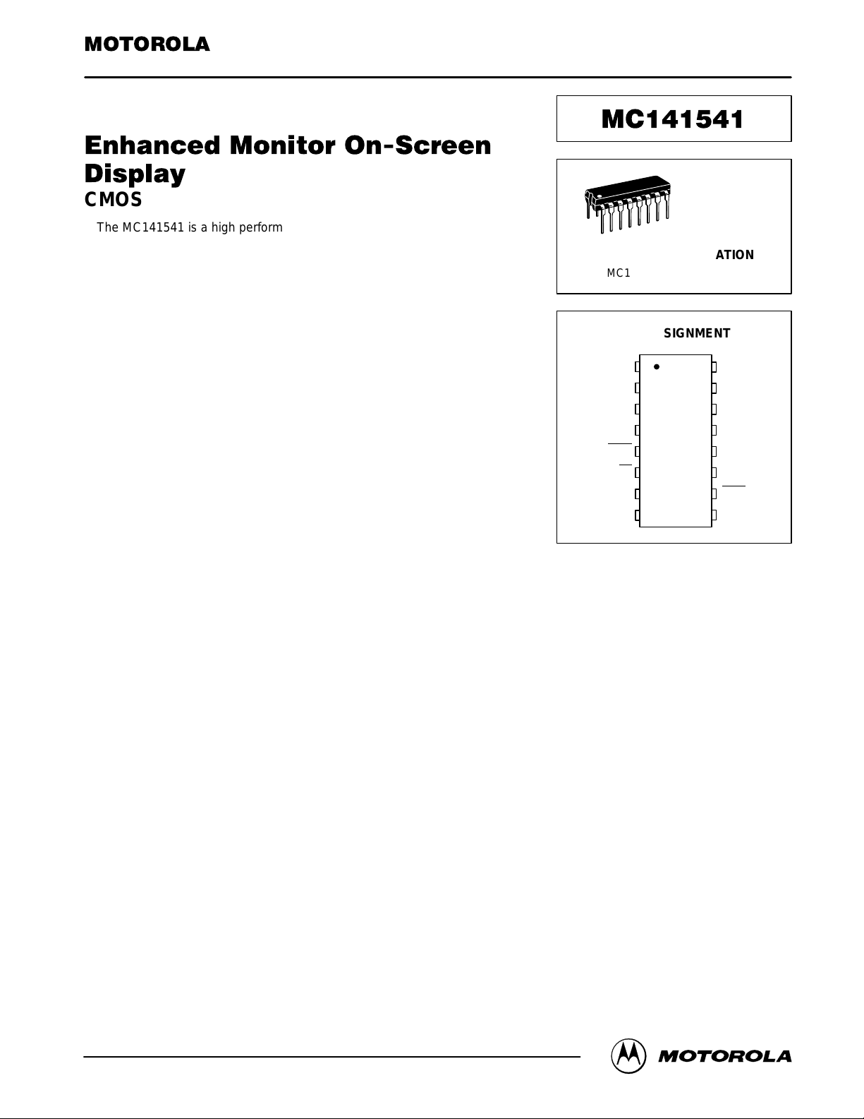
P SUFFIX
PLASTIC DIP
CASE 648
ORDERING INFORMATION
MC141541P Plastic DIP
PIN ASSIGNMENT
V
SS(A)
VCO
RP
V
)
DD(A
HFLB
SS
SDA(MOSI)
SCL(SCK)
1
2
3
4
6
7
8
16
15
14
13
125
11
10
9
V
SS
R
G
B
FBKG
HTONE/
PWMCK
VFLB
V
DD
REV 1
2/97 TN97031200
Motorola, Inc. 1997
MOTOROLA
MC141541
1
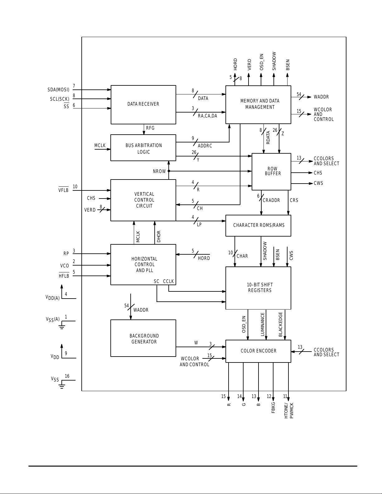
SDA(MOSI)
SCL(SCK)
SS
VFLB
7
8
6
10
CHS
VERD
MCLK
8
DATA RECEIVER
RFG
BUS ARBITRATION
LOGIC
NROW
VERTICAL
CONTROL
CIRCUIT
BLOCK DIAGRAM
8
DATA
3
RA,CA,DA
9
ADDRC
26
Y
4
R
5
CH
4
LP
HORD
5
8
MEMORY AND DA T A
MANAGEMENT
CHARACTER ROMS/RAMS
8
ROW
BUFFER
6
CRADDR
SHADOW
26
RDATA
Z
OSD_EN
VERD
BSEN
54
15
13
CRS
WADDR
WCOLOR
AND
CONTROL
CCOLORS
AND SELECT
CHS
CWS
V
DD(A)
VSS(A)
V
DD
V
SS
RP
VCO
HFLB
4
1
9
16
MCLK
3
2
5
HORIZONTAL
CONTROL
AND PLL
54
WADDR
BACKGROUND
GENERAT OR
SC
DHOR
CCLK
5
HORD
W
3
WCOLOR
AND CONTROL
15
10
CHAR
10–BIT SHIFT
REGISTERS
OSD_EN
COLOR ENCODER
G
R
BSEN
SHADOW
LUMINANCE
B
FBKG
CWS
BLACKEDGE
13
1115 14 13 12
PWMCK
HTONE/
CCOLORS
AND SELECT
MC141541
2
MOTOROLA
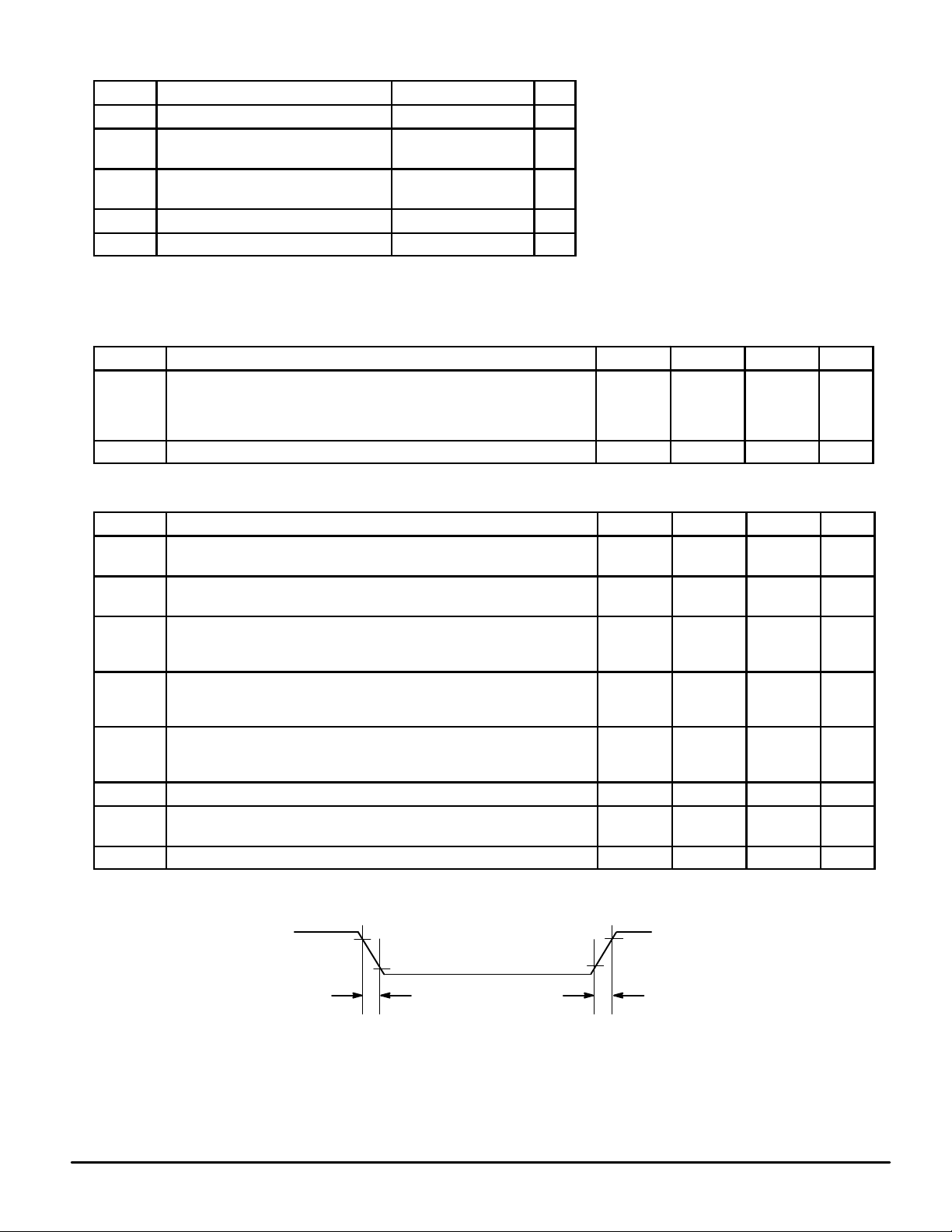
ABSOLUTE MAXIMUM RATINGS Voltage Referenced to V
Symbol
V
V
T
NOTE: Maximum Ratings are those values beyond which damage to the device may occur.
Supply Voltage – 0.3 to + 7.0 V
DD
Input Voltage VSS – 0.3 to
in
Id Current Drain per Pin Excluding V
and V
Operating Temperature Range 0 to 85 °C
Ta
Storage Temperature Range – 65 to + 150 °C
stg
Functional operation should be restricted to the limits in the Electrical Characteristics tables or Pin Description section.
Characteristic Value Unit
DD
SS
SS
V
VDD + 0.3
25 mA
This device contains circuitry to protect the
inputs against damage due to high static voltages or electric fields; however, it is advised that
normal precautions be taken to avoid applications of any voltage higher than the maximum
rated voltages to this high impedance circuit.
For proper operation it is recommended that
Vin and V
(Vin or V
be tied to an appropriate logic voltage level (e.g.,
either VSS or VDD). Unused outputs must be left
open.
be constrained to the range VSS ≤
out
) ≤ VDD. Unused inputs must always
out
AC ELECTRICAL CHARACTERISTICS (V
Symbol Characteristic Min Typ Max Unit
Output Signal (R, G, B, FBKG and HTONE/PWMCK) C
t
r
t
f
F
HFLB
DC CHARACTERISTICS V
Symbol Characteristic Min Typ Max Unit
V
OH
V
OL
V
IL
V
IH
V
IL
V
IH
V
IL
V
IH
I
II
I
II
I
DD
Figure 1
Rise Time
Fall Time
HFLB Input Frequency — — 110 kHz
= V
DD
DD(A)
High Level Output Voltage
I
= – 5 mA
out
Low Level Output Voltage
I
= 5 mA
out
Digital Input Voltage (Not Including SDA and SCL)
Logic Low
Logic High
Input Voltage of Pin SDA and SCL in SPI Mode
Logic Low
Logic High
Input Voltage of Pin SDA and SCL in M_BUS Mode
Logic Low
Logic High
High–Z Leakage Current (R, G, B and FBKG) – 10 — + 10 µA
Input Current (Not Including RP, VCO, R, G, B, FBKG and
HTONE/PWMCK)
Supply Current (No Load on Any Output) — — + 15 mA
= V
DD
= 5.0 V ± 10%, VSS = V
= 5.0 V, VSS = V
DD(A)
= 0 V, TA = 25°C, Voltage Referenced to VSS)
SS(A)
= 30 pF, see
load
= 0 V, TA = 25°C, Voltage Referenced to V
SS(A)
—
—
VDD – 0.8 — — V
— — VSS + 0.4 V
—
0.7 V
DD
—
0.7 V
DD
—
0.7 V
DD
– 10 — + 10 µA
—
—
—
—
—
—
—
—
SS
0.3 V
0.3 V
0.3 V
6
6
—
—
—
DD
DD
DD
ns
ns
V
V
V
V
V
V
MOTOROLA
90%
10%
tf tr
Figure 1. Switching Characteristics
90%
10%
MC141541
3
PIN DESCRIPTIONS
ООООО
ООООО
ООООО
V
Analog ground for PLL operation is separated from digital
ground for optimal performance.
VCO (Pin 2)
(Pin 1)
SS(A)
This pin provides the signal ground to the PLL circuitry.
er the external R, G, and B amplifiers’ gain to achieve a
transparent windowing effect. If the PWMCK_EN bit is set to
1 via M_BUS or SPI, this pin is changed to a mode–dependent clock output with 50/50 duty cycle and is synchronous
with the input horizontal synchronization signal at Pin 5. The
frequency is dependent on the mode in which the EMOSD is
currently running. The exact frequencies in the different resolution modes are described in Table 1.
Pin 2 is a control voltage input to regulate an internal oscillator frequency . See the Application Diagram for the application values used.
RP (Pin 3)
An external RC network is used to bias an internal VCO to
resonate at the specific dot frequency . The maximum voltage
at Pin 3 should not exceed 3.5 V at any condition. See the
Application Diagram for the application values used.
V
DD(A)
(Pin 4)
Pin 4 is a positive 5 V supply for PLL circuitry . Analog power for PLL is separated from digital power for optimal performance.
(Pin 5)
HFLB
This pin inputs a negative polarity horizontal synchronize
signal pulse to phase lock an internal system clock generated by the on–chip VCO circuit.
(Pin 6)
SS
This input pin is part of the SPI serial interface. An active
low signal generated by the master device enables this slave
device to accept data. This pin should be pulled high to terminate the SPI communication. If M_BUS is employed as the
serial interface, this pin should be tied to either V
DD
or V
SS
SDA (MOSI) (Pin 7)
Data and control messages are being transmitted to this
chip from a host MCU via one of the two serial bus systems.
With either protocol, this wire is configured as a uni–directional data line. (Detailed description of these two protocols
will be discussed in the M_BUS and SPI sections).
SCL (SCK) (Pin 8)
A separate synchronizing clock input from the transmitter
is required for either protocol. Data is read at the rising edge
of each clock signal.
VDD (Pin 9)
This is the power pin for the digital logic of the chip.
(Pin 10)
VFLB
Similar to Pin 5, this pin inputs a negative polarity vertical
synchronize signal pulse.
HTONE/PWMCK (Pin 11)
This is a multiplexed pin. When the PWMCK_EN bit is
cleared after power–on or by the MCU, this pin is HTONE
and outputs a logic high during windowing except when
graphics or characters are being displayed. It is used to low-
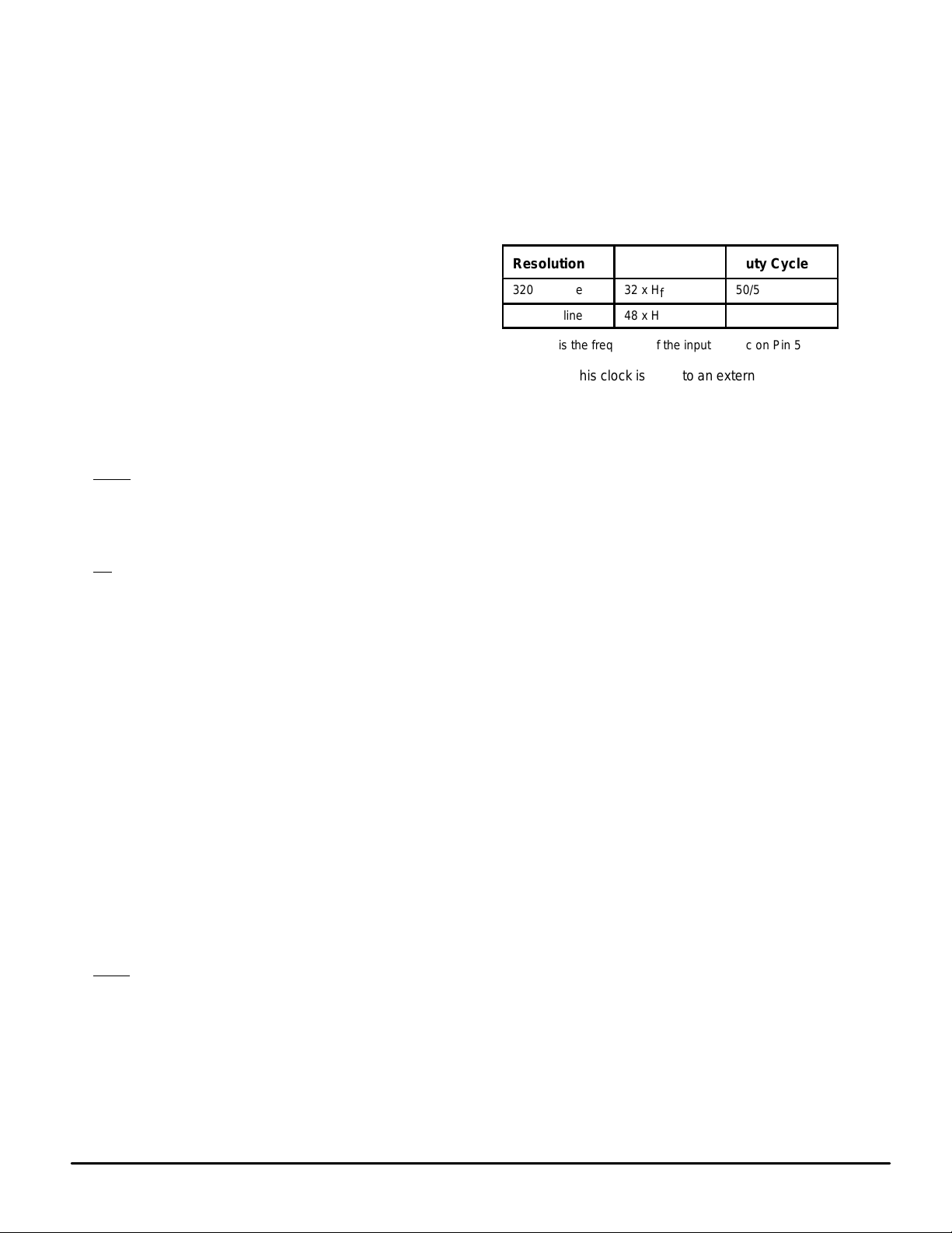
T able 1. PWM CLK Frequency
Resolution
320 dots/line
480 dots/line
NOTE: Hf is
the frequency of the input H sync on Pin 5.
Frequency
32 x H
f
48 x H
f
Duty Cycle
50/50
50/50
Typically, this clock is fed into an external pulse width modulation module as its clock source. Because of the synchronization between PWM clock and H sync, a better
performance on the PWM controlled functions can be
achieved.
FBKG (Pin 12)
This pin outputs a logic high while displaying characters or
windows when the FBKGC bit in the frame control register is
0, and output a logic high only while displaying characters
when the FBKGC bit is 1. It is defaulted to high–impedance
state after power–on, or when there is no output. An external
10 kΩ resistor pulled low is recommended to avoid level toggling caused by hand effect when there is no output.
B,G,R (Pins 13,14,15)
EMOSD color output is TTL level RGB to the host monitor.
These three signals are active high output pins that are in a
.
high–impedance state when EMOSD is disabled.
VSS (Pin 16)
This is the ground pin for the digital logic of the chip.
SYSTEM DESCRIPTION
MC141541 is a full–screen memory architecture. Refresh
is performed by the built–in circuitry after a screenful of display data has been loaded through the serial bus. Only
changes to the display data need to be input afterward.
Serial data, which includes screen mapping address, display information, and control messages, are transmitted via
one of the two serial buses: M_BUS or SPI (mask option).
These two sets of buses are multiplexed onto a single set of
wires. Standard parts offer M_BUS transmission. Parts
which offer SPI transmission mode must be specially
manufactured as custom parts.
Data is received from the serial port and stored by the
memory management circuit. Line data is stored in a row
buffer for display and refreshing. During this storing and retrieving cycle, bus arbitration logic patrols the internal traffic
to make sure that no crashes occur between the slower serial bus receiver and the fast ‘screen–refresh’ circuitry. After
the full–screen display data is received through one of the
serial communication interfaces, the link can be terminated if
a change of the display is not required.
MC141541
4
MOTOROLA
The bottom half of the Block Diagram contains the hardware functions for the entire system. It performs all the
EMOSD functions such as programmable vertical length
(from 16 lines to 63 lines), display clock generation (which is
phase locked to the incoming horizontal sync signal at Pin 5
), bordering or shadowing, and multiple windowing.
HFLB
COMMUNICATION PROTOCOLS
M_BUS Serial Communication
This is a two–wire serial communication link that is fully
compatible with the IIC bus system. It consists of an SDA bidirectional data line and an SCL clock input line. Data is sent
from a transmitter (master) to a receiver (slave) via the SDA
line, and is synchronized with a transmitter clock on the SCL
line at the receiving end. The maximum data rate is limited to
100 kbps and the default chip address is $7A, but is hardware changeable by mask set.
Operating Procedure
Figure 2 shows the M_BUS transmission format. The master initiates a transmission routine by generating a start
condition followed by a slave address byte. Once the address is properly identified, the slave will respond with an acknowledge signal by pulling the SDA line low during the ninth
SCL clock. Each data byte that follows must be eight bits
long, plus the acknowledge bit, for a total of nine bits. Appropriate row and column address information and display
data can be downloaded sequentially in one of the three
transmission formats described in the Data Transmission
Formats section. In the cases of no acknowlege or completion of data transfer, the master will generate a stop condition
to terminate the transmission routine. Note that the OSD_EN
bit must be set after all the display information has been sent,
in order to activate the EMOSD circuitry of MC141541 so that
the received information can be displayed.
DATA BYTES
ACK
SDA
CHIP ADDRESS
ACK
Display RAM and Control Registers
After the proper identification by the receiving device, a
data train of arbitrary length is transmitted from the master.
There are three transmission formats from (a) to (c) as stated
below. The data train in each sequence consists of row address (R), column address (C), and display information (I), as
shown in Figure 3. In format (a), display information data
must be preceded with the corresponding row address and
column address. This format is particularly suitable for updating small amounts of data between different rows. However,
if the current information byte has the same row address as
the one before, format (b) is recommended.
row addr col addr info
Figure 3. Data Packet
For a full–screen pattern change that requires a massive
information update, or during power–up, most of the row and
column addresses of either (a) or (b) formats will be consecutive. Therefore, a more efficient data transmission format (c)
should be applied. This sends the RAM starting row and column addresses once only, and then treats all subsequent
data as display information. The row and column addresses
will be automatically incremented internally for each display
information data from the starting location.
The data transmission formats are:
(a) R – > C – > I – > R – > C – > I – > . . . . . . . . .
(b) R – > C – > I – > C – > I – > C – > I. . . . . . .
(c) R – > C – > I – > I – > I – > . . . . . . . . . . . . .
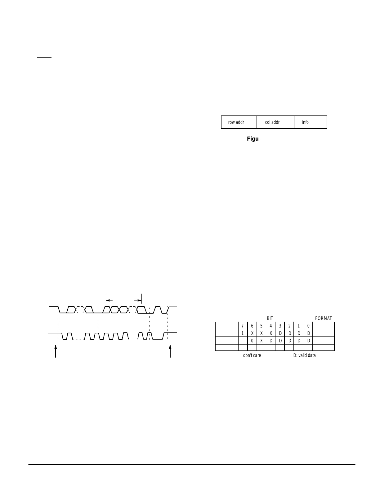
T o dif ferentiate the row and column addresses when transferring data from master, the MSB (most significant bit) is set,
as in Figure 4: ‘1’ to represent row, and ‘0’ for column address. Furthermore, to distinguish the column address between formats (a), (b), and (c), the sixth bit of the column
address is set to ‘1’ which represents format (c), and ‘0’ for
format (a) or (b). However, there is some limitation on using
mixed formats during a single transmission. It is permissible
to change the format from (a) to (b), or from (a) to (c), or from
(b) to (a), but not from (c) back to (a) or (b).
SCL
1
STAR T CONDITION
9 82–7
STOP CONDITION
Figure 2. M_BUS Format
DA TA TRANSMISSION FORMATS
In this enhanced version MOSD, both display RAM, control registers, and character RAM fonts need to be programmed after power–on. The arrangement of the display
RAM and control registers is on the row–column basis, while
the character RAM is on the segment–line basis. Although
the address basis is different, the data downloading protocols are very similar and will be described in the following
sections.
MOTOROLA
ADDRESS
ROW
COLUMN
COLUMN
X: don’t care D: valid data
FORMATBIT
01234567
a, b, c
DDDDXXX1
a, b
DDDDDX00
DDDDDX10
c
Figure 4. Row & Column Address Bit Patterns
Character RAM
The structure of eight character RAM fonts is shown in Figure 5. They occupy the font number from 0 to 7. Because of
the 10 x 16 dot matrix font, each font is broken down into two
segments in the horizontal direction and 16 lines in the vertical direction. Therefore, there are five dots that need to be
defined for each specified segment–line location. This 5–bit
data forms the lower five bits of the information data byte and
the higher three bits are ignored. Because there are 16 segments (two segments per font) and 16 lines, both the segment and line addresses are four bits wide.
MC141541
5
 Loading...