

Motorola MC141540P Datasheet
MC141540
1
MOTOROLA
CMOS
The MC141540 is a high performance HCMOS device designed to interface
with a microcontroller unit to allow colored symbols or characters to be
displayed on a color monitor. The on–chip PLL allows both multi–system
operation and self–generation of system timing. It also minimizes the MCU’s
burden through its built–in 273 bytes display/control RAM. By storing a full
screen of data and control information, this device has a capability to carry out
‘screen–refresh’ without MCU supervision.
Since there is no spacing between characters, special graphics–oriented
characters can be generated by combining two or more character blocks.
Special functions such as character bordering or shadowing, multi–level
windows, double height and double width, and programmable vertical length of
character can also be incorporated. Furthermore, neither massive information
update nor extremely high data transmission rate are expected for normal on–
screen display operation, and serial protocols are implemented in lieu of any
parallel formats to achieve minimum pin count.
• Fixed Resolution: 320 (CGA) Dots per Line
• Fully Programmable Character Array of 10 Rows by 24 Columns
• 273 Bytes Direct Mapping Display RAM Architecture
• Internal PLL Generates a Wide–Ranged System Clock
• For High–End Monitor Application, Maximum Horizontal Frequency is
100 kHz (32 MHz Dot Clock)
• Programmable Vertical Height of Character to Meet Multi–Sync
Requirement
• Programmable Vertical and Horizontal Positioning for Display Center
• 128 Characters and Graphic Symbols ROM
• 10 x 16 Dot Matrix Character
• Character–by–Character Color Selection
• A Maximum of Four Selectable Colors per Row
• Double Character Height and Double Character Width
• Character Bordering or Shadowing
• Three Fully Programmable Background Windows with Overlapping
Capability
• Single Positive 5 V Supply
• MC141540P4 is a Replacement for XC141540P with Two Symbols Added
in ROM Addresses ‘5C’ and ‘5E’
Order this document
by MC141540/D
SEMICONDUCTOR TECHNICAL DATA
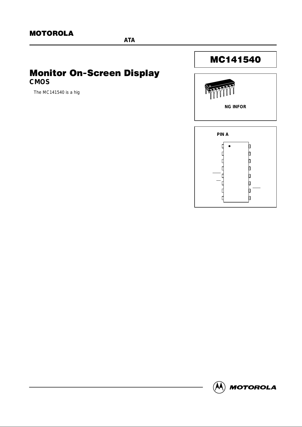
PIN ASSIGNMENT
P SUFFIX
PLASTIC DIP
CASE 648
ORDERING INFORMATION
MC141540P4 Plastic DIP
13
14
15
16
9
10
11
125
4
3
2
1
8
7
6
FBKG
B
G
R
V
SS
V
DD
VFLB
HTONE
V
DD(A
)
RP
VCO
SCL(SCK)
SDA(MOSI)
SS
HFLB
V
SS(A)
Motorola, Inc. 1997
REV 1
2/97 TN97031200
MC141540
MOTOROLA
2
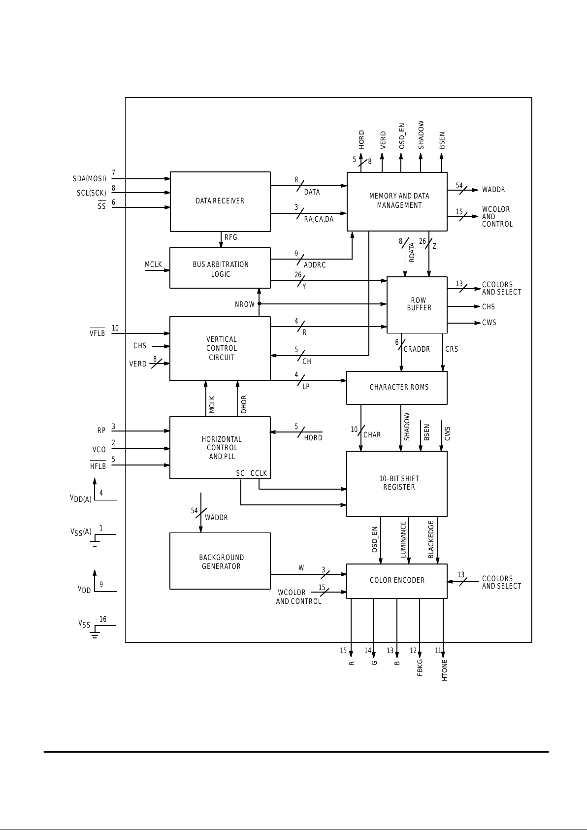
BLOCK DIAGRAM
DATA RECEIVER
BUS ARBITRATION
VERTICAL
CONTROL
CIRCUIT
HORIZONTAL
CONTROL
BACKGROUND
GENERAT OR
COLOR ENCODER
10–BIT SHIFT
REGISTER
CHARACTER ROMS
ROW
BUFFER
LOGIC
WADDR
WCOLOR
CCOLORS
CHS
CWS
CRS
WCOLOR
AND CONTROL
CCOLORS
AND SELECT
WADDR
SC
HORD
5
CCLK
DHOR
LP
4
BLACKEDGE
MCLK
SDA(MOSI)
RP
VCO
SCL(SCK)
DATA
RA,CA,DA
RFG
ADDRC
Y
9
3
8
7
8
6
10
3
2
5
54
1115 14 13 12
3
W
R
CHS
54
15
13
8
5
26
NROW
15
13
CWS
SHADOW
FBKG
HTONE
B
G
R
CHAR
CRADDR
OSD_EN
VERD
HORD
RDATA
LUMINANCE
BSEN
SHADOW
BSEN
OSD_EN
5
CH
4
AND PLL
AND
CONTROL
8
VERD
4
Z
26
8
AND SELECT
6
10
9
1
16
V
DD
VSS(A)
V
DD(A)
MCLK
V
SS
MEMORY AND DATA
MANAGEMENT
SS
VFLB
HFLB
MC141540
3
MOTOROLA
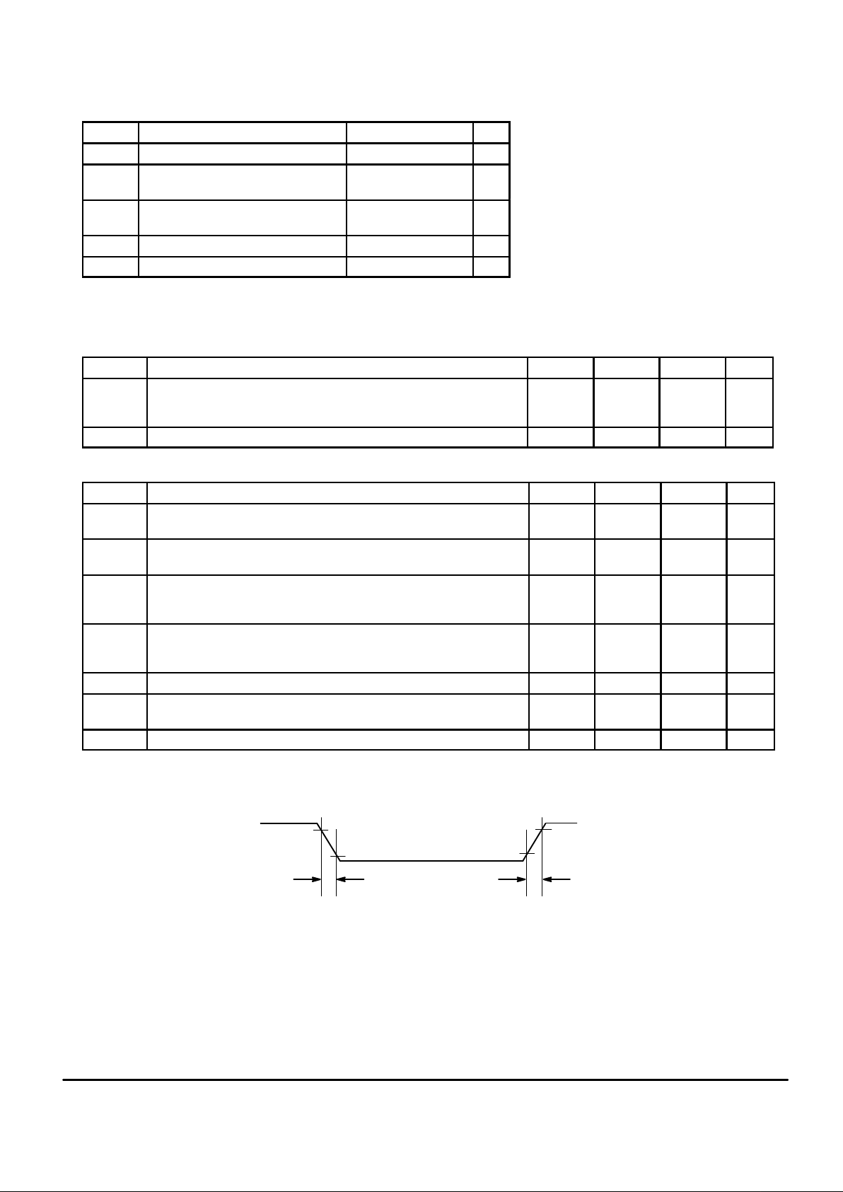
ABSOLUTE MAXIMUM RATINGS Voltage Referenced to V
SS
Symbol
Characteristic Value Unit
V
DD
Supply Voltage – 0.3 to + 7.0 V
V
in
Input Voltage VSS – 0.3 to
VDD + 0.3
V
Id Current Drain per Pin Excluding V
DD
and V
SS
25 mA
Ta
Operating Temperature Range 0 to 85 °C
T
stg
Storage Temperature Range – 65 to + 150 °C
NOTE: Maximum Ratings are those values beyond which damage to the device may occur.
Functional operation should be restricted to the limits in the Electrical Characteristics tables or Pin Description section.
AC ELECTRICAL CHARACTERISTICS (V
DD
= V
DD(A)
= 5.0 V , VSS = V
SS(A)
= 0 V, TA = 25°C, Voltage Referenced to VSS)
Symbol Characteristic Min Typ Max Unit
t
r
t
f
Output Signal (R, G, B, FBKG and HTONE) C
load
= 30 pF, see Figure 1
Rise Time
Fall Time
—
—
—
—
10
10
ns
ns
F
HFLB
HFLB Input Frequency — — 100 kHz
DC CHARACTERISTICS V
DD
= V
DD(A)
= 5.0 V ± 10%, VSS = V
SS(A)
= 0 V, TA = 25°C, Voltage Referenced to V
SS
Symbol Characteristic Min Typ Max Unit
V
OH
High Level Output Voltage
I
out
= – 5 mA
VDD – 0.8 — — V
V
OL
Low Level Output Voltage
I
out
= 5 mA
— — VSS + 0.4 V
V
IL
V
IH
Digital Input Voltage (Not Including SDA and SCL)
Logic Low
Logic High
—
0.7 V
DD
—
—
0.3 V
DD
—
V
V
V
IL
V
IH
Input Voltage of Pin SDA and SCL in SPI Mode
Logic Low
Logic High
—
0.7 V
DD
—
—
0.3 V
DD
—
V
V
I
II
High–Z Leakage Current (R, G, B and FBKG) – 10 — + 10 µA
I
II
Input Current (Not Including RP, VCO, R, G, B, FBKG and HTONE)
– 10 — + 10 µA
I
DD
Supply Current (No Load on Any Output) — 9* — mA
*Not a guaranteed limit.
90%
10%
90%
10%
tf tr
Figure 1. Switching Characteristics
This device contains circuitry to protect the
inputs against damage due to high static voltages or electric fields; however, it is advised that
normal precautions be taken to avoid applications of any voltage higher than the maximum
rated voltages to this high impedance circuit.
For proper operation it is recommended that
Vin and V
out
be constrained to the range VSS ≤
(Vin or V
out
) ≤ VDD. Unused inputs must always
be tied to an appropriate logic voltage level (e.g.,
either VSS or VDD). Unused outputs must be left
open.

MC141540
MOTOROLA
4
PIN DESCRIPTIONS
V
SS(A)
(Pin 1)
This pin provides the signal ground to the PLL circuitry.
Analog ground for PLL operation is separated from digital
ground for optimal performance.
VCO (Pin 2)
Pin 2 is a control voltage input to regulate an internal oscillator frequency. See the Application Diagram for the application values used.
RP (Pin 3)
An external RC network is used to bias an internal VCO to
resonate at the specific dot frequency. The value of the resistor for this pin should be adjusted in order to set the pin voltage to around half VDD. See the Application Diagram for the
application values used.
V
DD(A)
(Pin 4)
Pin 4 is a positive 5 V supply for PLL circuitry. Analog power for PLL is separated from digital power for optimal performance.
HFLB
(Pin 5)
This pin inputs a negative polarity horizontal synchronize
signal pulse to phase lock an internal system clock generated by the on–chip VCO circuit.
SS
(Pin 6)
This input pin is part of the SPI serial interface. An active
low signal generated by the master device enables this slave
device to accept data. This pin should be pulled high to terminate the SPI communication.
SDA (MOSI) (Pin 7)
Data and control messages are being transmitted to this
chip from a host MCU via this wire, which is configured as a
uni–directional data line. (Detailed description of these two
protocols will be discussed in the SPI section).
SCL (SCK) (Pin 8)
A separate synchronizing clock input from the transmitter
is required for either protocol. Data is read at the rising edge
of each clock signal.
VDD (Pin 9)
This is the power pin for the digital logic of the chip.
VFLB
(Pin 10)
Similar to Pin 5, this pin inputs a negative polarity vertical
synchronize signal pulse.
HTONE (Pin 11)
This pin outputs a logic high during windowing except
when graphics or characters are being displayed. It is used
to lower the external R, G, and B amplifiers’ gain to achieve a
transparent windowing effect.
FBKG (Pin 12)
This pin outputs a logic high while displaying characters or
windows when the FBKGC bit in the frame control register is
0, and output a logic high only while displaying characters
when the FBKGC bit is 1. It is defaulted to high–impedance
state after power–on, or when there is no output. An external
10 kΩ resistor pulled low is recommended to avoid level toggling caused by hand effect when there is no output.
B,G,R (Pins 13,14,15)
MOSD color output is TTL level RGB to the host monitor.
These three signals are active high output pins that are in a
high–impedance state when MOSD is disabled.
VSS (Pin 16)
This is the ground pin for the digital logic of the chip.
SYSTEM DESCRIPTION
MC141540 is a full–screen memory architecture. Refresh
is performed by the built–in circuitry after a screenful of display data has been loaded through the serial bus. Only
changes to the display data need to be input afterward.
Serial data, which includes screen mapping address, display information, and control messages, are transmitted via
the SPI bus. Figure 2 contains the SPI protocol operating
procedure.
Data is received from the serial port and stored by the
memory management circuit. Line data is stored in a row
buffer for display and refreshing. During this storing and retrieving cycle, bus arbitration logic patrols the internal traffic
to make sure that no crashes occur between the slower serial bus receiver and the fast ‘screen–refresh’ circuitry. After
the full–screen display data is received through one of the
serial communication interfaces, the link can be terminated if
a change of the display is not required.
The bottom half of the block diagram contains the hardware functions for the entire system. It performs all the
MOSD functions such as programmable vertical length (from
16 lines to 63 lines), display clock generation (which is phase
locked to the incoming horizontal sync signal at Pin 5 HFLB
),
bordering or shadowing, and multiple windowing.
COMMUNICATION PROTOCOLS
Serial Peripheral Interface (SPI)
SPI is a three–wire serial communication link that requires
separate clock (SCK) and data (MOSI) lines. In addition, an
SS
slave select pin is controlled by the master transmitter to
initiate the receiver.
Operating Procedure
To initiate SPI transmission, the SS
pin is pulled low by the
master device to enable MC141540 to accept data. The SS
input line must be a logic low prior to the occurrence of SCK,
and remain low until and after the last (eighth) SCK cycle. After all data has been sent, the SS
pin is then pulled high by
the master to terminate the transmission. No slave address
is needed for SPI. Hence, row and column address information and display data can be sent immediately after the SPI is
initiated.
 Loading...