

Motorola MC14017BD, MC14017BCL, MC14017BCP Datasheet
MOTOROLA CMOS LOGIC DATAMC14017B
74
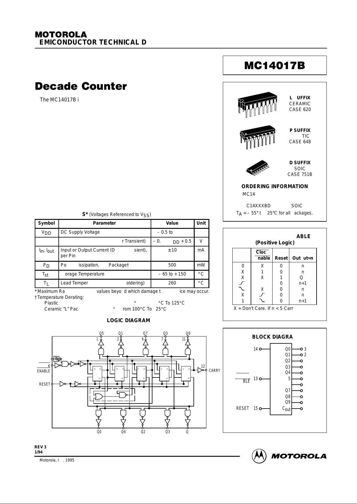
The MC14017B is a five–stage Johnson decade counter with built–in code
converter. High speed operation and spike–free outputs are obtained by use
of a Johnson decade counter design. The ten decoded outputs are normally
low, and go high only at their appropriate decimal time period. The output
changes occur on the positive–going edge of the clock pulse. This part can
be used in frequency division applications as well as decade counter or
decimal decode display applications.
• Fully Static Operation
• DC Clock Input Circuit Allows Slow Rise Times
• Carry Out Output for Cascading
• Divide–by–N Counting
• Supply Voltage Range = 3.0 Vdc to 18 Vdc
• Capable of Driving Two Low–power TTL Loads or One Low–power
Schottky TTL Load Over the Rated Temperature Range
• Pin–for–Pin Replacement for CD4017B
• Triple Diode Protection on All Inputs
MAXIMUM RATINGS* (Voltages Referenced to V
SS
)
Symbol
Parameter
Value
Unit
V
DD
DC Supply Voltage
– 0.5 to + 18.0
V
Vin, V
out
Input or Output Voltage (DC or Transient)
– 0.5 to VDD + 0.5
V
lin, l
out
Input or Output Current (DC or Transient),
per Pin
± 10
mA
P
D
Power Dissipation, per Package†
500
mW
T
stg
Storage Temperature
– 65 to + 150
_
C
T
L
Lead Temperature (8–Second Soldering)
260
_
C
*Maximum Ratings are those values beyond which damage to the device may occur.
†Temperature Derating:
Plastic “P and D/DW” Packages: – 7.0 mW/_C From 65_C To 125_C
Ceramic “L” Packages: – 12 mW/_C From 100_C To 125_C
LOGIC DIAGRAM
CLOCK
CLOCK
ENABLE
CARRY
RESET
Q5 Q1 Q7 Q3 Q9
117621
12
Q0 Q6 Q2 Q3 Q4
3 5 4 9 10
14
13
15
C
C
D
R R
Q
Q
C
C
D
R R
Q
Q
C
C
D
R R
Q
Q
C
C
D
R R
Q
Q
C
C
D
R R
Q
Q
SEMICONDUCTOR TECHNICAL DATA
Motorola, Inc. 1995
REV 3
1/94
L SUFFIX
CERAMIC
CASE 620
ORDERING INFORMATION
MC14XXXBCP Plastic
MC14XXXBCL Ceramic
MC14XXXBD SOIC
TA = – 55° to 125°C for all packages.
P SUFFIX
PLASTIC
CASE 648
D SUFFIX
SOIC
CASE 751B
BLOCK DIAGRAM
FUNCTIONAL TRUTH TABLE
(Positive Logic)
Clock Decode
Clock Enable
Reset Output=n
0 X 0 n
X 1 0 n
X X 1 Q0
0 0 n+1
X 0 n
X 0 n
1 0 n+1
X = Don’t Care. If n < 5 Carry = “1”,
Otherwise = “0”.
CLOCK
CLOCK
ENABLE
RESET
14
13
15 C
out
Q9
Q8
Q7
Q6
Q5
Q4
Q3
Q2
Q1
Q0 3
2
4
7
10
1
5
6
9
11
12
VDD = PIN 16
VSS = PIN 8
MOTOROLA CMOS LOGIC DATA
75
MC14017B
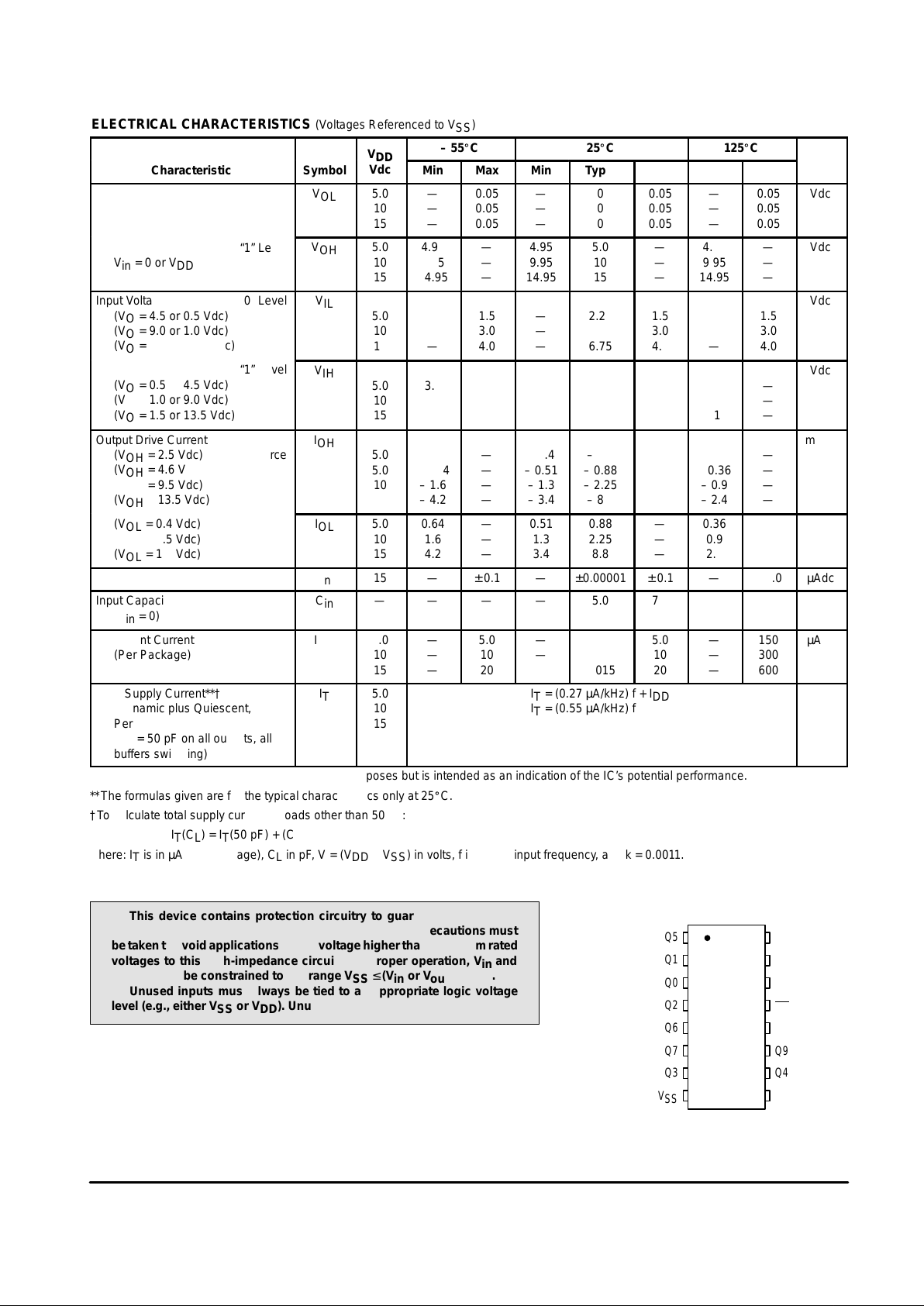
ELECTRICAL CHARACTERISTICS (Voltages Referenced to V
SS
)
V
– 55_C
25_C
125_C
Characteristic
Symbol
V
DD
Vdc
Min
Max
Min
Typ #
Max
Min
ÎÎÎ
ÎÎÎ
ÎÎÎ
Max
Unit
Output Voltage
“0” Level
Vin = VDD or 0
V
OL
5.0
10
15
—
—
—
0.05
0.05
0.05
—
—
—
0
0
0
0.05
0.05
0.05
—
—
—
ÎÎÎ
ÎÎÎ
ÎÎÎ
ÎÎÎ
0.05
0.05
0.05
Vdc
“1” Level
Vin = 0 or V
DD
V
OH
5.0
10
15
4.95
9.95
14.95
—
—
—
4.95
9.95
14.95
5.0
10
15
—
—
—
4.95
9.95
14.95
ÎÎÎ
ÎÎÎ
ÎÎÎ
ÎÎÎ
ÎÎÎ
—
—
—
Vdc
Input Voltage
“0” Level
(VO = 4.5 or 0.5 Vdc)
(VO = 9.0 or 1.0 Vdc)
(VO = 13.5 or 1.5 Vdc)
V
IL
5.0
10
15
—
—
—
1.5
3.0
4.0
—
—
—
2.25
4.50
6.75
1.5
3.0
4.0
—
—
—
ÎÎÎ
ÎÎÎ
ÎÎÎ
ÎÎÎ
ÎÎÎ
1.5
3.0
4.0
Vdc
“1” Level
(VO = 0.5 or 4.5 Vdc)
(VO = 1.0 or 9.0 Vdc)
(VO = 1.5 or 13.5 Vdc)
V
IH
5.0
10
15
3.5
7.0
11
—
—
—
3.5
7.0
11
2.75
5.50
8.25
—
—
—
3.5
7.0
11
ÎÎÎ
ÎÎÎ
ÎÎÎ
ÎÎÎ
ÎÎÎ
—
—
—
Vdc
Output Drive Current
(VOH = 2.5 Vdc) Source
(VOH = 4.6 Vdc)
(VOH = 9.5 Vdc)
(VOH = 13.5 Vdc)
I
OH
5.0
5.0
10
15
– 3.0
– 0.64
– 1.6
– 4.2
—
—
—
—
– 2.4
– 0.51
– 1.3
– 3.4
– 4.2
– 0.88
– 2.25
– 8.8
—
—
—
—
– 1.7
– 0.36
– 0.9
– 2.4
ÎÎÎ
ÎÎÎ
ÎÎÎ
ÎÎÎ
ÎÎÎ
—
—
—
—
mAdc
(VOL = 0.4 Vdc) Sink
(VOL = 0.5 Vdc)
(VOL = 1.5 Vdc)
I
OL
5.0
10
15
0.64
1.6
4.2
—
—
—
0.51
1.3
3.4
0.88
2.25
8.8
—
—
—
0.36
0.9
2.4
ÎÎÎ
ÎÎÎ
ÎÎÎ
ÎÎÎ
ÎÎÎ
—
—
—
mAdc
Input Current
I
in
15
—
± 0.1
—
±0.00001
± 0.1
—
ÎÎÎ
ÎÎÎ
ÎÎÎ
± 1.0
µAdc
Input Capacitance
(Vin = 0)
C
in
—
—
—
—
5.0
7.5
—
ÎÎÎ
ÎÎÎ
ÎÎÎ
—
pF
Quiescent Current
(Per Package)
I
DD
5.0
10
15
—
—
—
5.0
10
20
—
—
—
0.005
0.010
0.015
5.0
10
20
—
—
—
ÎÎÎ
ÎÎÎ
ÎÎÎ
ÎÎÎ
ÎÎÎ
150
300
600
µAdc
Total Supply Current**†
(Dynamic plus Quiescent,
Per Package)
(CL = 50 pF on all outputs, all
buffers switching)
I
T
5.0
10
15
IT = (0.27 µA/kHz) f + I
DD
IT = (0.55 µA/kHz) f + I
DD
IT = (0.83 µA/kHz) f + I
DD
µAdc
#Data labelled “Typ” is not to be used for design purposes but is intended as an indication of the IC’s potential performance.
**The formulas given are for the typical characteristics only at 25_C.
†To calculate total supply current at loads other than 50 pF:
IT(CL) = IT(50 pF) + (CL – 50) Vfk
where: IT is in µA (per package), CL in pF, V = (VDD – VSS) in volts, f in kHz is input frequency, and k = 0.0011.
This device contains protection circuitry to guard against damage
due to high static voltages or electric fields. However, precautions must
be taken to avoid applications of any voltage higher than maximum rated
voltages to this high-impedance circuit. For proper operation, Vin and
V
out
should be constrained to the range VSS ≤ (Vin or V
out
) ≤ VDD.
Unused inputs must always be tied to an appropriate logic voltage
level (e.g., either VSS or VDD). Unused outputs must be left open.
PIN ASSIGNMENT
13
14
15
16
9
10
11
125
4
3
2
1
8
7
6
C
out
CE
CLOCK
RESET
V
DD
Q8
Q4
Q9
Q2
Q0
Q1
Q5
V
SS
Q3
Q7
Q6
MOTOROLA CMOS LOGIC DATAMC14017B
76
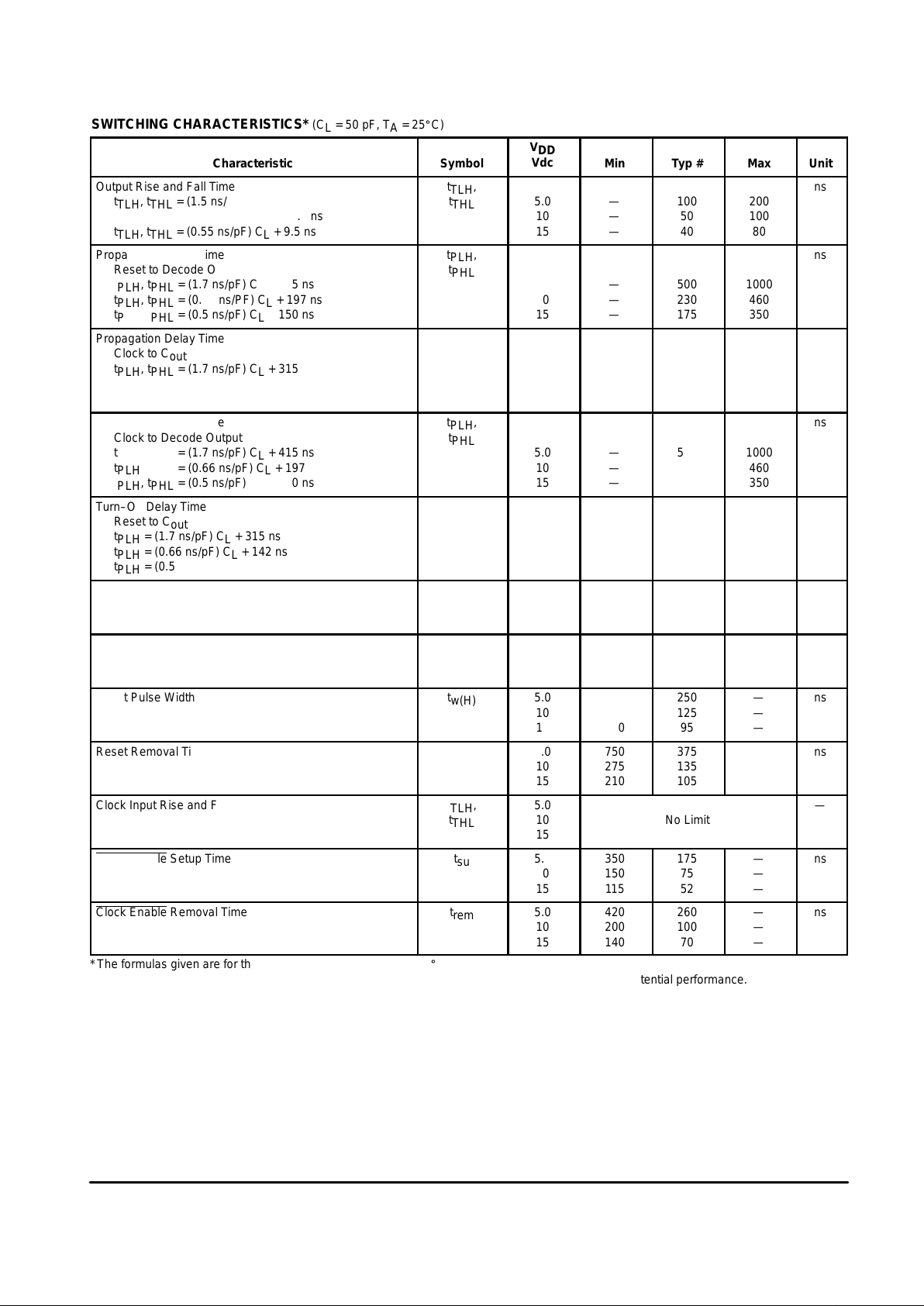
SWITCHING CHARACTERISTICS* (C
L
= 50 pF, TA = 25_C)
Characteristic
ÎÎÎÎ
ÎÎÎÎ
ÎÎÎÎ
ÎÎÎÎ
Symbol
V
DD
Vdc
ÎÎÎÎ
ÎÎÎÎ
ÎÎÎÎ
ÎÎÎÎ
Min
Typ #
Max
Unit
Output Rise and Fall Time
t
TLH
, t
THL
= (1.5 ns/pF) CL + 25 ns
t
TLH
, t
THL
= (0.75 ns/pF) CL + 12.5 ns
t
TLH
, t
THL
= (0.55 ns/pF) CL + 9.5 ns
ÎÎÎÎ
ÎÎÎÎ
ÎÎÎÎ
ÎÎÎÎ
ÎÎÎÎ
t
TLH
,
t
THL
5.0
10
15
ÎÎÎÎ
ÎÎÎÎ
ÎÎÎÎ
ÎÎÎÎ
ÎÎÎÎ
—
—
—
100
50
40
200
100
80
ns
Propagation Delay Time
Reset to Decode Output
t
PLH
, t
PHL
= (1.7 ns/pF) CL + 415 ns
t
PLH
, t
PHL
= (0.66 ns/PF) CL + 197 ns
t
PLH
, t
PHL
= (0.5 ns/pF) CL + 150 ns
ÎÎÎÎ
ÎÎÎÎ
ÎÎÎÎ
ÎÎÎÎ
ÎÎÎÎ
t
PLH
,
t
PHL
5.0
10
15
ÎÎÎÎ
ÎÎÎÎ
ÎÎÎÎ
ÎÎÎÎ
ÎÎÎÎ
—
—
—
500
230
175
1000
460
350
ns
Propagation Delay Time
Clock to C
out
t
PLH
, t
PHL
= (1.7 ns/pF) CL + 315 ns
t
PLH
, t
PHL
= (0.66 ns/pF) CL + 142 ns
t
PLH
, t
PHL
= (0.5 ns/pF) CL + 100 ns
ÎÎÎÎ
ÎÎÎÎ
ÎÎÎÎ
ÎÎÎÎ
ÎÎÎÎ
ÎÎÎÎ
t
PLH
,
t
PHL
5.0
10
15
ÎÎÎÎ
ÎÎÎÎ
ÎÎÎÎ
ÎÎÎÎ
ÎÎÎÎ
ÎÎÎÎ
—
—
—
400
175
125
800
350
250
ns
Propagation Delay Time
Clock to Decode Output
t
PLH
, t
PHL
= (1.7 ns/pF) CL + 415 ns
t
PLH
, t
PHL
= (0.66 ns/pF) CL + 197 ns
t
PLH
, t
PHL
= (0.5 ns/pF) CL + 150 ns
ÎÎÎÎ
ÎÎÎÎ
ÎÎÎÎ
ÎÎÎÎ
ÎÎÎÎ
ÎÎÎÎ
t
PLH
,
t
PHL
5.0
10
15
ÎÎÎÎ
ÎÎÎÎ
ÎÎÎÎ
ÎÎÎÎ
ÎÎÎÎ
ÎÎÎÎ
—
—
—
500
230
175
1000
460
350
ns
Turn–Off Delay Time
Reset to C
out
t
PLH
= (1.7 ns/pF) CL + 315 ns
t
PLH
= (0.66 ns/pF) CL + 142 ns
t
PLH
= (0.5 ns/pF) CL + 100 ns
ÎÎÎÎ
ÎÎÎÎ
ÎÎÎÎ
ÎÎÎÎ
ÎÎÎÎ
t
PLH
5.0
10
15
ÎÎÎÎ
ÎÎÎÎ
ÎÎÎÎ
ÎÎÎÎ
ÎÎÎÎ
—
—
—
400
175
125
800
350
250
ns
Clock Pulse Width
ÎÎÎÎ
ÎÎÎÎ
ÎÎÎÎ
ÎÎÎÎ
t
w(H)
5.0
10
15
ÎÎÎÎ
ÎÎÎÎ
ÎÎÎÎ
ÎÎÎÎ
250
100
75
125
50
35
—
—
—
ns
Clock Frequency
ÎÎÎÎ
ÎÎÎÎ
ÎÎÎÎ
ÎÎÎÎ
ÎÎÎÎ
f
cl
5.0
10
15
ÎÎÎÎ
ÎÎÎÎ
ÎÎÎÎ
ÎÎÎÎ
ÎÎÎÎ
—
—
—
5.0
12
16
2.0
5.0
6.7
MHz
Reset Pulse Width
ÎÎÎÎ
ÎÎÎÎ
ÎÎÎÎ
ÎÎÎÎ
t
w(H)
5.0
10
15
ÎÎÎÎ
ÎÎÎÎ
ÎÎÎÎ
ÎÎÎÎ
500
250
190
250
125
95
—
—
—
ns
Reset Removal Time
ÎÎÎÎ
ÎÎÎÎ
ÎÎÎÎ
ÎÎÎÎ
t
rem
5.0
10
15
ÎÎÎÎ
ÎÎÎÎ
ÎÎÎÎ
ÎÎÎÎ
750
275
210
375
135
105
—
—
—
ns
Clock Input Rise and Fall Time
ÎÎÎÎ
ÎÎÎÎ
ÎÎÎÎ
ÎÎÎÎ
ÎÎÎÎ
t
TLH
,
t
THL
5.0
10
15
ОООООООООО
ОООООООООО
ОООООООООО
ОООООООООО
ОООООООООО
No Limit
—
Clock Enable Setup Time
ÎÎÎÎ
ÎÎÎÎ
ÎÎÎÎ
ÎÎÎÎ
t
su
5.0
10
15
ÎÎÎÎ
ÎÎÎÎ
ÎÎÎÎ
ÎÎÎÎ
350
150
115
175
75
52
—
—
—
ns
Clock Enable Removal Time
ÎÎÎÎ
ÎÎÎÎ
ÎÎÎÎ
ÎÎÎÎ
t
rem
5.0
10
15
ÎÎÎÎ
ÎÎÎÎ
ÎÎÎÎ
ÎÎÎÎ
420
200
140
260
100
70
—
—
—
ns
*The formulas given are for the typical characteristics only at 25_C.
#Data labelled “Typ” is not to be used for design purposes but is intended as an indication of the IC’s potential performance.
 Loading...