

MOTOROLA MC14016BDR2, MC14016BF, MC14016BFEL, MC14016BCP, MC14016BD Datasheet
MC14016B
Quad Analog Switch/
Quad Multiplexer
The MC14016B quad bilateral switch is constructed with MOS
P–channel and N–channel enhancement mode devices in a single
monolithic structure. Each MC14016B consists of four independent
switches capable of controlling either digital or analog signals. The
quad bilateral switch is used in signal gating, chopper, modulator,
demodulator and CMOS logic implementation.
• Diode Protection on All Inputs
• Supply Voltage Range = 3.0 Vdc to 18 Vdc
• Linearized Transfer Characteristics
• Low Noise — 12 nV/√Cycle, f ≥ 1.0 kHz typical
• Pin–for–Pin Replacements for CD4016B, CD4066B (Note improved
transfer characteristic design causes more parasitic coupling
capacitance than CD4016)
• For Lower R
The MC14066B
• This Device Has Inputs and Outputs Which Do Not Have ESD
Protection. Antistatic Precautions Must Be T aken.
MAXIMUM RATINGS (Voltages Referenced to V
Symbol Parameter Value Unit
V
DD
Vin, V
out
I
in
I
SW
P
D
T
A
T
stg
T
L
2. Maximum Ratings are those values beyond which damage to the device
may occur.
3. Temperature Derating:
Plastic “P and D/DW” Packages: – 7.0 mW/_C From 65_C To 125_C
This device contains protection circuitry to guard against damage due to high
static voltages or electric fields. However, precautions must be taken to avoid
applications of any voltage higher than maximum rated voltages to this
high–impedance circuit. For proper operation, Vin and V
to the range V
Unused inputs must always be tied to an appropriate logic voltage level (e.g.,
either V
or VDD). Unused outputs must be left open.
SS
, Use The HC4016 High–Speed CMOS Device or
ON
) (Note 2.)
SS
DC Supply Voltage Range –0.5 to +18.0 V
Input or Output Voltage Range
(DC or Transient)
Input Current (DC or Transient)
per Control Pin
Switch Through Current ±25 mA
Power Dissipation,
per Package (Note 3.)
Ambient Temperature Range –55 to +125 °C
Storage Temperature Range –65 to +150 °C
Lead Temperature
(8–Second Soldering)
v (Vin or V
SS
) v VDD.
out
–0.5 to VDD + 0.5 V
±10 mA
500 mW
260 °C
should be constrained
out
http://onsemi.com
MARKING
DIAGRAMS
14
PDIP–14
P SUFFIX
CASE 646
SOIC–14
D SUFFIX
CASE 751A
SOEIAJ–14
F SUFFIX
CASE 965
A = Assembly Location
WL or L = Wafer Lot
YY or Y = Year
WW or W = Work Week
MC14016BCP
AWLYYWW
1
14
14016B
AWLYWW
1
14
MC14016B
AWLYWW
1
ORDERING INFORMATION
Device Package Shipping
MC14016BCP PDIP–14 2000/Box
MC14016BD SOIC–14
MC14016BDR2 SOIC–14 2500/Tape & Reel
MC14016BF SOEIAJ–14
MC14016BFEL SOEIAJ–14 See Note 1.
1. For ordering information on the EIAJ version of
the SOIC packages, please contact your local
ON Semiconductor representative.
55/Rail
See Note 1.
Semiconductor Components Industries, LLC, 2000
March, 2000 – Rev . 3
1 Publication Order Number:
MC14016B/D
MC14016B
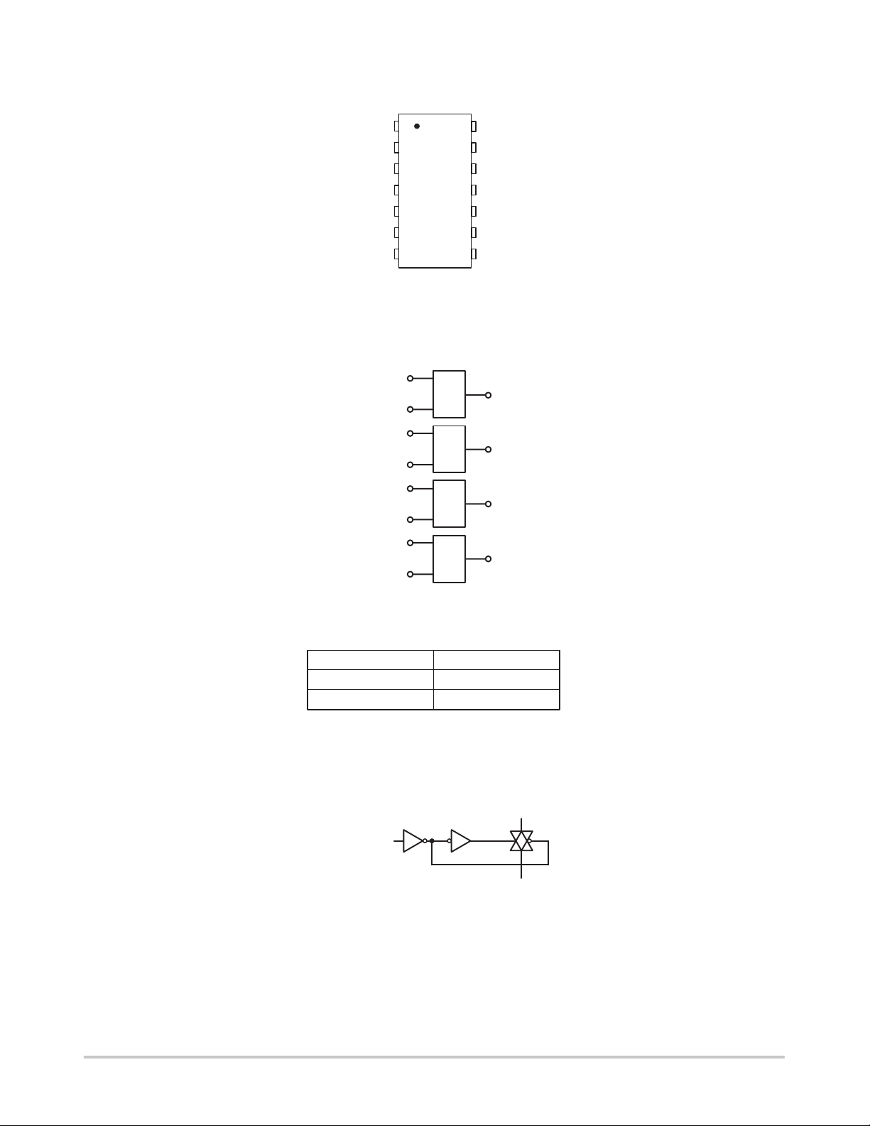
PIN ASSIGNMENT
IN 1
OUT 1
OUT 2
IN 2
CONTROL 2
CONTROL 3
V
SS
BLOCK DIAGRAM
CONTROL 1
IN 1
CONTROL 2
IN 2
CONTROL 3
IN 3
CONTROL 4
IN 4
1
2
3
4
6
7
14
13
12
11
105
9
8
V
DD
CONTROL 1
CONTROL 4
IN 4
OUT 4
OUT 3
IN 3
13
2
1
OUT 1
5
3
4
OUT 2
6
9
8
OUT 3
12
10
11
OUT 4
V
= PIN 14
DD
V
= PIN 7
SS
Control Switch
0 = V
SS
1 = V
DD
LOGIC DIAGRAM
(1/4 OF DEVICE SHOWN)
CONTROL
LOGIC DIAGRAM RESTRICTIONS
V
≤ Vin ≤ V
SS
VSS ≤ V
DD
≤ V
out
DD
Off
On
OUT
IN
http://onsemi.com
2
MC14016B
ÎÎÎÎ
V
DD
ÎÎ
Î
Î
Î
Î
ÎÎ
ÎÎ
Î
Î
Î
Î
Î
Î
Î
Î
ÎÎ
ÎÎ
Î
Î
Î
Î
Î
Î
ÎÎ
Î
Î
Î
Î
Î
Î
Î
Î
Î
Î
Î
Î
ÎÎ
ÎÎ
ÎÎ
ÎÎ
Î
Î
Î
Î
Î
Î
Î
Î
Î
Î
Î
Î
Î
Î
Î
Î
Î
Î
Î
Î
Î
Î
ÎÎ
ÎÎ
Î
Î
Î
Î
Î
Î
Î
Î
Î
Î
Î
Î
Î
Î
Î
Î
Î
Î
ÎÎ
ÎÎ
ÎÎ
ÎÎ
Î
Î
Î
Î
Î
Î
Î
Î
Î
Î
Î
Î
Î
Î
Î
Î
Î
Î
Î
Î
ÎÎ
ÎÎ
Î
Î
Î
Î
Î
Î
Î
Î
ÎÎ
ÎÎ
Î
Î
Î
Î
Î
Î
Î
Î
Î
Î
Î
Î
Î
Î
ÎÎ
ÎÎ
ÎÎ
Î
Î
Î
Î
Î
Î
Î
Î
Î
Î
Î
Î
Î
Î
Î
Î
Î
Î
Î
Î
Î
Î
Î
Î
ÎÎ
ÎÎ
ÎÎ
ÎÎ
Î
Î
Î
Î
Î
Î
Î
Î
Î
Î
Î
Î
Î
Î
Î
Î
Î
Î
Î
Î
Î
Î
Î
Î
Î
Î
ÎÎ
ÎÎ
ÎÎ
Î
Î
Î
Î
Î
Î
Î
Î
Î
Î
Î
Î
ELECTRICAL CHARACTERISTICS (Voltages Referenced to V
Characteristic
Input Voltage
Control Input
ООООООООО
ОООООООООÎÎÎÎÎ
Input Current Control
Input Capacitance
ООООООООО
Control
Switch Input
ООООООООО
Switch Output
ООООООООО
Feed Through
Quiescent Current
(Per Package)
ООООООООО
“ON” Resistance
ООООООООО
(V
= VDD, RL = 10 kΩ)
C
= + 5.0 Vdc)
(V
in
ООООООООО
(V
= – 5.0 Vdc) VSS = – 5.0 Vdc
in
ООООООООО
(V
= ± 0.25 Vdc)
in
(5.)
(Vin = + 7.5 Vdc)
(V
= – 7.5 Vdc) VSS = – 7.5 Vdc
in
ООООООООО
= ± 0.25 Vdc)
(V
in
(Vin = + 10 Vdc)
(V
= + 0.25 Vdc) VSS = 0 Vdc
ООООООООО
in
= + 5.6 Vdc)
(V
in
(Vin = + 15 Vdc)
ООООООООО
(V
= + 0.25 Vdc) VSS = 0 Vdc
in
= + 9.3 Vdc)
(V
in
ООООООООО
∆ “ON” Resistance
Figure
Î
Î
Î
Î
Î
Î
Î
Î
ÎÎÎÎÎÎ
ÎÎÎÎÎÎ
Î
Î
1
—
—
2,3
4,5,6
—
Symbol
V
IL
ÎÎ
V
IH
I
in
C
in
ÎÎ
ÎÎ
ÎÎ
I
DD
ÎÎ
R
ON
ÎÎ
ÎÎ
ÎÎ
ÎÎ
ÎÎ
∆R
ON
V
Vdc
5.0
10
Î
15
5.0
10
Î
15
15
Î
—
—
Î
—
Î
—
5.0
10
Î
15
Î
Î
Î
5.0
7.5
10
Î
15
Î
SS
)
Min
—
—
—
—
—
—
—
—
—
—
—
—
—
—
—
—
—
—
—
—
—
—
—
—
—
—
– 55_C
Î
Î
±0.1
Î
Î
Î
0.25
Î
Î
Î
Î
Î
Î
Î
Î
Max
—
—
—
—
—
—
—
—
—
—
0.5
1.0
600
600
600
360
360
360
600
600
600
360
360
360
Min
—
—
Î
—
3.0
8.0
Î
13
—
Î
—
—
Î
—
Î
—
—
—
Î
—
—
Î
—
—
Î
—
Î
—
—
—
Î
—
—
—
Î
—
—
Î
—
—
Î
25_C
(4.)
Typ
1.5
1.5
ÎÎ
1.5
2.0
6.0
ÎÎ
11
±0.00001
ÎÎ
5.0
5.0
ÎÎ
5.0
ÎÎ
0.2
0.0005
0.0010
ÎÎ
0.0015
ÎÎ
300
ÎÎ
300
ÎÎ
280
240
240
ÎÎ
180
260
310
ÎÎ
310
260
ÎÎ
260
300
ÎÎ
Max
0.9
0.9
Î
0.9
—
—
Î
—
±0.1
Î
—
—
Î
—
Î
—
0.25
0.5
Î
1.0
Î
660
Î
660
Î
660
400
400
Î
400
660
660
Î
660
400
Î
400
400
Î
Min
—
—
—
—
—
—
—
—
—
—
—
—
—
—
—
—
—
—
—
—
—
—
—
—
—
—
—
—
125_C
Î
Î
Î
Î
Î
Î
Î
Î
Î
Î
Î
Î
Î
Between any 2 circuits in a common
ООООООООО
package
(V
= VDD)
C
ООООООООО
(V
= ± 5.0 Vdc, VSS = – 5.0 Vdc)
in
ООООООООО
(V
= ± 7.5 Vdc, VSS = – 7.5 Vdc)
in
Input/Output Leakage Current
(V
= VSS)
C
ООООООООО
= + 7.5, V
(V
in
(V
= – 7.5, V
ООООООООО
in
= – 7.5 Vdc)
out
= + 7.5 Vdc)
out
Î
Î
Î
—
Î
Î
ÎÎ
ÎÎ
ÎÎ
—
ÎÎ
ÎÎ
5.0
7.5
7.5
7.5
Î
Î
Î
Î
Î
Î
Î
—
Î
—
Î
—
—
Î
—
—
±0.1
±0.1
Î
Î
—
Î
—
Î
—
—
Î
ÎÎ
ÎÎ
15
ÎÎ
10
ÎÎ
±0.0015
±0.0015
ÎÎ
Î
Î
—
Î
—
Î
±0.1
± 0.1——
Î
Î
Î
—
Î
—
Î
Î
NOTE: All unused inputs must be returned to VDD or VSS as appropriate for the circuit application.
4. Data labelled “Typ” is not to be used for design purposes but is intended as an indication of the IC’s potential performance.
5. For voltage drops across the switch (∆V
current out of the switch may contain both V
Maximum Ratings are exceeded. (See first page of this data sheet.) Reference Figure 14.
) > 600 mV ( > 300 mV at high temperature), excessive VDD current may be drawn; i.e., the
switch
and switch input components. The reliability of the device will be unaffected unless the
DD
Max
—
—
—
—
—
—
± 1.0
—
—
—
—
7.5
15
30
840
840
840
520
520
520
840
840
840
520
520
520
—
—
± 1.0
± 1.0
Unit
Vdc
Î
Vdc
Î
µAdc
pF
Î
Î
Î
µAdc
Î
Ohms
Î
Î
Î
Î
Î
Î
Î
Ohms
Î
Î
Î
µAdc
Î
Î
http://onsemi.com
3
MC14016B
Î
Î
Î
Î
Î
Î
Î
Î
Î
Î
Î
Î
Î
Î
Î
Î
Î
Î
Î
Î
Î
Î
Î
Î
Î
Î
Î
Î
Î
Î
Î
Î
Î
Î
Î
Î
Î
Î
Î
Î
Î
Î
Î
Î
Î
Î
Î
Î
Î
Î
Î
Î
Î
Î
Î
Î
Î
Î
Î
Î
Î
Î
Î
Î
Î
Î
Î
Î
Î
Î
Î
Î
Î
Î
Î
Î
Î
Î
Î
Î
Î
Î
Î
Î
Î
Î
Î
Î
Î
Î
Î
Î
Î
Î
Î
Î
Î
Î
Î
Î
Î
Î
Î
Î
Î
Î
Î
Î
Î
Î
Î
Î
Î
Î
Î
Î
Î
Î
Î
Î
Î
Î
Î
Î
Î
Î
Î
Î
Î
Î
Î
Î
Î
Î
Î
Î
Î
Î
Î
Î
Î
Î
Î
Î
Î
Î
Î
Î
Î
Î
Î
Î
Î
Î
Î
Î
Î
Î
Î
Î
Î
Î
Î
Î
Î
Î
Î
Î
Î
Î
Î
Î
Î
Î
Î
Î
Î
Î
Î
Î
Î
Î
–50dB)
(6.)
(C
= 50 pF, TA = 25_C)
L
Figure
10,11
12,13
Symbol
Î
Î
Î
Î
Î
—
Î
Î
Î
7
Î
8
Î
Î
9
Î
t
PLH
t
t
PHZ
t
PLZ
t
PZH
t
PHL
PZL
—
,
,
,
,
ÎÎ
ÎÎ
ÎÎ
ÎÎ
ÎÎ
—
Î
Î
ÎÎ
ÎÎ
—
Î
ÎÎÎÎÎÎ
—
Î
Î
12
Î
Î
Î
Î
Î
—
Î
Î
—
Î
Î
Î
Î
ÎÎ
ÎÎ
ÎÎ
ÎÎ
ÎÎ
ÎÎ
ÎÎ
BW
Î
Î
Î
Î
—
Î
Î
Î
Î
Î
Î
Î
Î
—
Î
Î
Î
Î
ÎÎ
ÎÎ
ÎÎ
ÎÎ
ÎÎ
ÎÎ
ÎÎ
ÎÎ
V
DD
Vdc
5.0
10
15
5.0
10
15
5.0
10
15
5.0
5.0
10
15
5.0
10
15
5.0
5.0
5.0
5.0
Min
Î
—
—
—
Î
—
Î
—
—
Î
—
—
Î
—
—
Î
Î
—
—
Î
—
—
—
Î
—
—
Î
Î
Î
—
Î
—
Î
—
—
Î
Î
Î
—
—
Î
—
Î
—
Î
Î
—
—
Î
—
Î
—
(7.)
Typ
ÎÎ
15
7.0
6.0
ÎÎ
34
ÎÎ
20
15
ÎÎ
30
50
ÎÎ
100
– 80
ÎÎ
ÎÎ
24
25
ÎÎ
30
12
12
ÎÎ
15
0.16
ÎÎ
ÎÎ
ÎÎ
2.3
ÎÎ
0.2
ÎÎ
0.1
0.05
ÎÎ
ÎÎ
ÎÎ
54
40
ÎÎ
38
ÎÎ
37
ÎÎ
ÎÎ
1250
140
ÎÎ
18
ÎÎ
2.0
Max
Î
45
15
12
Î
90
Î
45
35
Î
—
—
Î
—
—
Î
Î
—
—
Î
—
—
—
Î
—
—
Î
Î
Î
—
Î
—
Î
—
—
Î
Î
Î
—
—
Î
—
Î
—
Î
Î
—
—
Î
—
Î
—
ELECTRICAL CHARACTERISTICS
ОООООООООООООО
Propagation Delay Time (VSS = 0 Vdc)
V
to V
in
out
(VC = VDD, RL = 10 kΩ)
ОООООООООООООО
Control to Output
(V
v 10 Vdc, RL = 10 kΩ)
in
ОООООООООООООО
ОООООООООООООО
Crosstalk, Control to Output (VSS = 0 Vdc)
(V
= VDD, Rin = 10 kΩ, R
C
ОООООООООООООО
f = 1.0 kHz)
Crosstalk between any two switches (VSS = 0 Vdc)
(R
= 1.0 kΩ, f = 1.0 MHz,
L
ОООООООООООООО
crosstalk+20log
ОООООООООООООО
Noise Voltage (VSS = 0 Vdc)
(V
= VDD, f = 100 Hz)
C
ОООООООООООООО
(VC = VDD, f = 100 kHz)
ОООООООООООООО
Second Harmonic Distortion (VSS = – 5.0 Vdc)
ОООООООООООООО
(V
= 1.77 Vdc, RMS Centered @ 0.0 Vdc,
in
= 10 kΩ, f = 1.0 kHz)
R
L
ОООООООООООООО
Insertion Loss (VC = VDD, Vin = 1.77 Vdc,
V
= – 5.0 Vdc, RMS centered = 0.0 Vdc, f = 1.0 MHz)
SS
ОООООООООООООО
I
+
20log
loss
ОООООООООООООО
(RL = 1.0 kΩ)
ОООООООООООООО
(R
= 10 kΩ)
L
= 100 kΩ)
(R
L
ОООООООООООООО
(R
= 1.0 MΩ)
L
Bandwidth (– 3.0 dB)
(V
= VDD, Vin = 1.77 Vdc, VSS = – 5.0 Vdc,
ОООООООООООООО
C
RMS centered @ 0.0 Vdc)
ОООООООООООООО
= 1.0 kΩ)
(R
L
(R
= 10 kΩ)
ОООООООООООООО
L
(R
= 100 kΩ)
L
ОООООООООООООО
(R
= 1.0 MΩ)
L
OFF Channel Feedthrough Attenuation
(V
= – 5.0 Vdc)
SS
ОООООООООООООО
(V
= VSS, 20 log
C
ОООООООООООООО
(RL = 1.0 kΩ)
ОООООООООООООО
(R
= 10 kΩ)
L
= 100 kΩ)
(R
L
ОООООООООООООО
(R
= 1.0 MΩ)
L
Characteristic
V
10
V
V
out
)
10
V
in
V
10
V
out1
out2
out
in
= 10 kΩ,
out
)
+
6. The formulas given are for typical characteristics only at 25_C.
7. Data labelled “Typ” is not to be used for design purposes but is intended as an indication of the IC’s potential performance.
Unit
ÎÎ
ns
ÎÎ
ns
ÎÎ
ÎÎ
mV
ÎÎ
dB
ÎÎ
ÎÎ
nV/√Cycle
ÎÎ
ÎÎ
%
ÎÎ
ÎÎ
dB
ÎÎ
ÎÎ
ÎÎ
ÎÎ
MHz
ÎÎ
ÎÎ
ÎÎ
ÎÎ
kHz
ÎÎ
ÎÎ
ÎÎ
ÎÎ
http://onsemi.com
4
 Loading...