

Motorola MC14016BD, MC14016BCL, MC14016BCP Datasheet
MOTOROLA CMOS LOGIC DATA
65
MC14016B
The MC14016B quad bilateral switch is constructed with MOS P–channel
and N–channel enhancement mode devices in a single monolithic structure.
Each M C14016B c onsists o f four independent switches c apable of
controlling either digital or analog signals. The quad bilateral switch is used
in s ignal g ating, c hopper, modulator, demodulator and CMOS l ogic
implementation.
• Diode Protection on All Inputs
• Supply Voltage Range = 3.0 Vdc to 18 Vdc
• Linearized Transfer Characteristics
• Low Noise — 12 nV/√Cycle
, f ≥ 1.0 kHz typical
• Pin–for–Pin Replacements for CD4016B, CD4066B (Note improved
transfer characteristic design causes more parasitic coupling
capacitance than CD4016)
• For Lower RON, Use The HC4016 High–Speed CMOS Device or The
MC14066B
• This Device Has Inputs and Outputs Which Do Not Have ESD
Protection. Antistatic Precautions Must Be Taken.
MAXIMUM RATINGS* (Voltages Referenced to V
SS
)
Symbol
Parameter
Value
Unit
V
DD
DC Supply Voltage
– 0.5 to + 18.0
V
Vin, V
out
Input or Output Voltage (DC or Transient)
– 0.5 to VDD + 0.5
V
l
in
Input Current (DC or Transient),
per Control Pin
± 10
mA
I
sw
Switch Through Current
± 25
mA
P
D
Power Dissipation, per Package†
500
mW
T
stg
Storage Temperature
– 65 to + 150
_
C
T
L
Lead Temperature (8–Second Soldering)
260
_
C
*Maximum Ratings are those values beyond which damage to the device may occur.
†Temperature Derating:
Plastic “P and D/DW” Packages: – 7.0 mW/_C From 65_C To 125_C
Ceramic “L” Packages: – 12 mW/_C From 100_C To 125_C
This device contains protection circuitry to guard against damage
due to high static voltages or electric fields. However, precautions must
be taken to avoid applications of any voltage higher than maximum rated
voltages to this high-impedance circuit. For proper operation, Vin and
V
out
should be constrained to the range VSS ≤ (Vin or V
out
) ≤ VDD.
Unused inputs must always be tied to an appropriate logic voltage
level (e.g., either VSS or VDD). Unused outputs must be left open.
SEMICONDUCTOR TECHNICAL DATA
Motorola, Inc. 1995
REV 3
1/94
L SUFFIX
CERAMIC
CASE 632
ORDERING INFORMATION
MC14XXXBCP Plastic
MC14XXXBCL Ceramic
MC14XXXBD SOIC
TA = – 55° to 125°C for all packages.
P SUFFIX
PLASTIC
CASE 646
D SUFFIX
SOIC
CASE 751A
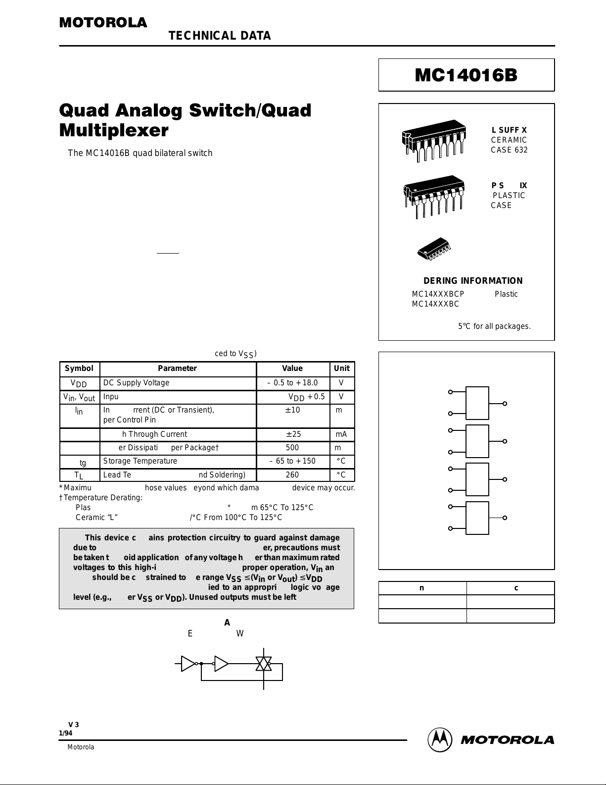
BLOCK DIAGRAM
CONTROL 1
IN 1
CONTROL 2
IN 2
CONTROL 3
IN 3
CONTROL 4
IN 4
OUT 1
OUT 2
OUT 3
OUT 4
13
1
5
4
6
8
12
11
2
3
9
10
VDD = PIN 14
VSS = PIN 7
Control Switch
0 = V
SS
Off
1 = V
DD
On
LOGIC DIAGRAM
(1/4 OF DEVICE SHOWN)
CONTROL
OUT
IN
LOGIC DIAGRAM RESTRICTIONS
VSS
≤
Vin ≤ V
DD
VSS
≤
V
out
≤ V
DD
MOTOROLA CMOS LOGIC DATAMC14016B
66
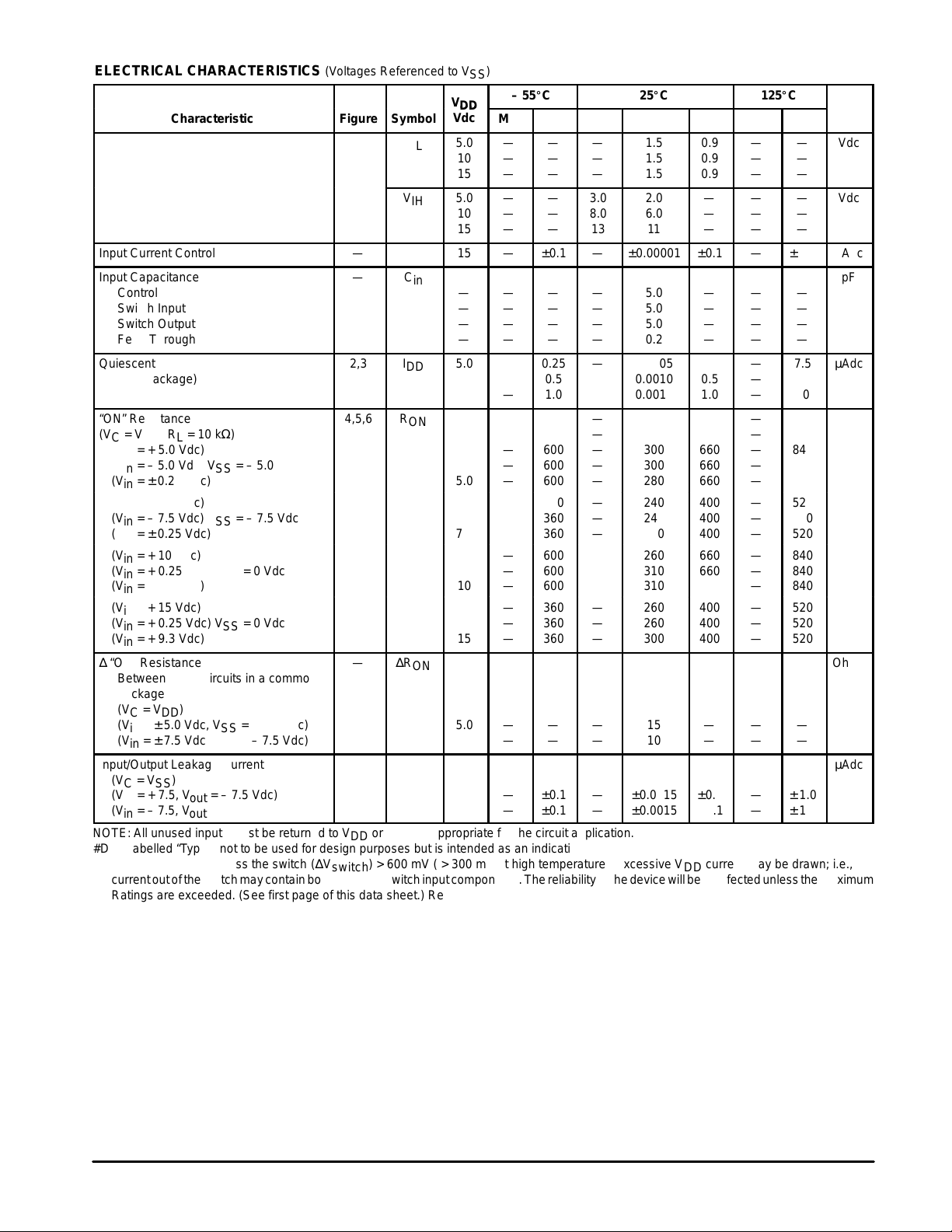
ELECTRICAL CHARACTERISTICS (Voltages Referenced to V
SS
)
V
– 55_C
25_C
125_C
Characteristic
Figure
Symbol
V
DD
Vdc
Min
Max
Min
ÎÎÎ
ÎÎÎ
ÎÎÎ
Typ #
Max
Min
Max
Unit
V
IL
5.0
10
15
—
—
—
—
—
—
—
—
—
ÎÎÎ
ÎÎÎ
ÎÎÎ
ÎÎÎ
1.5
1.5
1.5
0.9
0.9
0.9
—
—
—
—
—
—
Vdc
V
IH
5.0
10
15
—
—
—
—
—
—
3.0
8.0
13
ÎÎÎ
ÎÎÎ
ÎÎÎ
ÎÎÎ
ÎÎÎ
2.0
6.0
11
—
—
—
—
—
—
—
—
—
Vdc
Input Current Control
—
I
in
15
—
±0.1
—
ÎÎÎ
ÎÎÎ
ÎÎÎ
±0.00001
±0.1
—
± 1.0
µAdc
Input Capacitance
Control
Switch Input
Switch Output
Feed Through
—
C
in
—
—
—
—
—
—
—
—
—
—
—
—
—
—
—
—
ÎÎÎ
ÎÎÎ
ÎÎÎ
ÎÎÎ
ÎÎÎ
5.0
5.0
5.0
0.2
—
—
—
—
—
—
—
—
—
—
—
—
pF
Quiescent Current
(Per Package)
2,3
I
DD
5.0
10
15
—
—
—
0.25
0.5
1.0
—
—
—
ÎÎÎ
ÎÎÎ
ÎÎÎ
ÎÎÎ
ÎÎÎ
0.0005
0.0010
0.0015
0.25
0.5
1.0
—
—
—
7.5
15
30
µAdc
“ON” Resistance
(VC = VDD, RL = 10 kΩ)
(Vin = + 5.0 Vdc)
(Vin = – 5.0 Vdc) VSS = – 5.0 Vdc
(Vin = ± 0.25 Vdc)
4,5,6
R
ON
5.0
—
—
—
600
600
600
—
—
—
—
—
ÎÎÎ
ÎÎÎ
ÎÎÎ
ÎÎÎ
ÎÎÎ
300
300
280
660
660
660
—
—
—
—
—
840
840
840
Ohms
(Vin = + 7.5 Vdc)
(Vin = – 7.5 Vdc) VSS = – 7.5 Vdc
(Vin = ± 0.25 Vdc)
7.5
—
—
—
360
360
360
—
—
—
ÎÎÎ
ÎÎÎ
ÎÎÎ
ÎÎÎ
240
240
180
400
400
400
—
—
—
520
520
520
(Vin = + 10 Vdc)
(Vin = + 0.25 Vdc) VSS = 0 Vdc
(Vin = + 5.6 Vdc)
10
—
—
—
600
600
600
—
—
—
ÎÎÎ
ÎÎÎ
ÎÎÎ
ÎÎÎ
ÎÎÎ
260
310
310
660
660
660
—
—
—
840
840
840
(Vin = + 15 Vdc)
(Vin = + 0.25 Vdc) VSS = 0 Vdc
(Vin = + 9.3 Vdc)
15
—
—
—
360
360
360
—
—
—
ÎÎÎ
ÎÎÎ
ÎÎÎ
ÎÎÎ
260
260
300
400
400
400
—
—
—
520
520
520
∆ “ON” Resistance
Between any 2 circuits in a common
package
(VC = VDD)
(Vin = ± 5.0 Vdc, VSS = – 5.0 Vdc)
(Vin = ± 7.5 Vdc, VSS = – 7.5 Vdc)
—
∆R
ON
5.0
7.5——
—
—
—
—
ÎÎÎ
ÎÎÎ
ÎÎÎ
ÎÎÎ
ÎÎÎ
ÎÎÎ
15
10
—
—
—
—
—
—
Ohms
Input/Output Leakage Current
(VC = VSS)
(Vin = + 7.5, V
out
= – 7.5 Vdc)
(Vin = – 7.5, V
out
= + 7.5 Vdc)
—
—
7.5
7.5——
±0.1
±0.1——
ÎÎÎ
ÎÎÎ
ÎÎÎ
ÎÎÎ
ÎÎÎ
±0.0015
±0.0015
±0.1
± 0.1——
± 1.0
± 1.0
µAdc
NOTE: All unused inputs must be returned to VDD or VSS as appropriate for the circuit application.
#Data labelled “Typ” is not to be used for design purposes but is intended as an indication of the IC’s potential performance.
**For voltage drops across the switch (∆V
switch
) > 600 mV ( > 300 mV at high temperature), excessive VDD current may be drawn; i.e., the
current out of the switch may contain both VDD and switch input components. The reliability of the device will be unaffected unless the Maximum
Ratings are exceeded. (See first page of this data sheet.) Reference Figure 14.
Input Voltage
Control Input
1
MOTOROLA CMOS LOGIC DATA
67
MC14016B
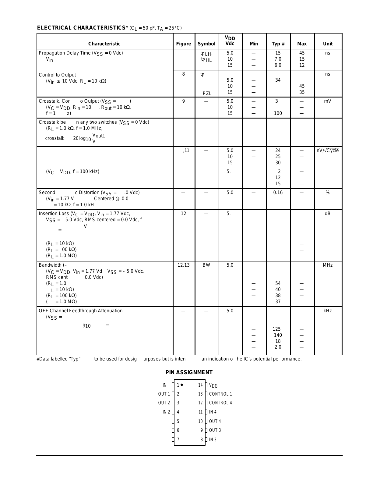
ELECTRICAL CHARACTERISTICS* (C
L
= 50 pF, TA = 25_C)
Characteristic
Figure
Symbol
V
DD
Vdc
Min
Typ #
ÎÎÎ
ÎÎÎ
ÎÎÎ
ÎÎÎ
Max
Unit
7
t
PLH
,
t
PHL
5.0
10
15
—
—
—
15
7.0
6.0
ÎÎÎ
ÎÎÎ
ÎÎÎ
ÎÎÎ
45
15
12
ns
v
10 Vdc, RL = 10 kΩ)
8
t
PHZ
,
t
PLZ
,
t
PZH
,
t
PZL
5.0
10
15
—
—
—
34
20
15
ÎÎÎ
ÎÎÎ
ÎÎÎ
ÎÎÎ
ÎÎÎ
90
45
35
ns
Crosstalk, Control to Output (VSS = 0 Vdc)
(VC = VDD, Rin = 10 kΩ, R
out
= 10 kΩ,
f = 1.0 kHz)
9
—
5.0
10
15
—
—
—
30
50
100
ÎÎÎ
ÎÎÎ
ÎÎÎ
ÎÎÎ
—
—
—
mV
Crosstalk between any two switches (VSS = 0 Vdc)
(RL = 1.0 kΩ, f = 1.0 MHz,
crosstalk+20log
10
V
out1
V
out2
)
—
—
5.0
—
– 80
ÎÎÎ
ÎÎÎ
ÎÎÎ
ÎÎÎ
ÎÎÎ
—
dB
Noise Voltage (VSS = 0 Vdc)
(VC = VDD, f = 100 Hz)
10,11
—
5.0
10
15
—
—
—
24
25
30
ÎÎÎ
ÎÎÎ
ÎÎÎ
ÎÎÎ
—
—
—
nV/√Cycle
(VC = VDD, f = 100 kHz)
5.0
10
15
—
—
—
12
12
15
ÎÎÎ
ÎÎÎ
ÎÎÎ
ÎÎÎ
ÎÎÎ
—
—
—
Second Harmonic Distortion (VSS = – 5.0 Vdc)
(Vin = 1.77 Vdc, RMS Centered @ 0.0 Vdc,
RL = 10 kΩ, f = 1.0 kHz)
—
—
5.0
—
0.16
ÎÎÎ
ÎÎÎ
ÎÎÎ
ÎÎÎ
—
%
Insertion Loss (VC = VDD, Vin = 1.77 Vdc,
VSS = – 5.0 Vdc, RMS centered = 0.0 Vdc, f = 1.0 MHz)
I
loss
+
20log
10
V
out
V
in
)
(RL = 1.0 kΩ)
(RL = 10 kΩ)
(RL = 100 kΩ)
(RL = 1.0 MΩ)
12
—
5.0
—
—
—
—
2.3
0.2
0.1
0.05
ÎÎÎ
ÎÎÎ
ÎÎÎ
ÎÎÎ
ÎÎÎ
ÎÎÎ
ÎÎÎ
—
—
—
—
dB
Bandwidth (– 3.0 dB)
(VC = VDD, Vin = 1.77 Vdc, VSS = – 5.0 Vdc,
RMS centered @ 0.0 Vdc)
(RL = 1.0 kΩ)
(RL = 10 kΩ)
(RL = 100 kΩ)
(RL = 1.0 MΩ)
12,13
BW
5.0
—
—
—
—
54
40
38
37
ÎÎÎ
ÎÎÎ
ÎÎÎ
ÎÎÎ
ÎÎÎ
ÎÎÎ
ÎÎÎ
—
—
—
—
MHz
OFF Channel Feedthrough Attenuation
(VSS = – 5.0 Vdc)
V
out
V
in
+
–50dB)
(RL = 1.0 kΩ)
(RL = 10 kΩ)
(RL = 100 kΩ)
(RL = 1.0 MΩ)
(VC = VSS, 20 log
10
—
—
5.0
—
—
—
—
1250
140
18
2.0
ÎÎÎ
ÎÎÎ
ÎÎÎ
ÎÎÎ
ÎÎÎ
ÎÎÎ
ÎÎÎ
—
—
—
—
kHz
#Data labelled “Typ” is not to be used for design purposes but is intended as an indication of the IC’s potential performance.
PIN ASSIGNMENT
11
12
13
14
8
9
105
4
3
2
1
7
6
OUT 4
IN 4
CONTROL 4
CONTROL 1
V
DD
IN 3
OUT 3
IN 2
OUT 2
OUT 1
IN 1
V
SS
CONTROL 3
CONTROL 2
Propagation Delay Time (VSS = 0 Vdc)
Vin to V
out
(VC = VDD, RL = 10 kΩ)
Control to Output
(Vin
 Loading...