

Motorola MC12093D, MC12093SD Datasheet
SEMICONDUCTOR
TECHNICAL DATA
MECL PLL COMPONENTS
÷2, ÷4, ÷8 LOW POWER
PRESCALER
WITH STAND–BY MODE
Order this document by MC12093/D
SD SUFFIX
PLASTIC PACKAGE
CASE 940
(SSOP–8)
PIN CONNECTIONS
D SUFFIX
PLASTIC PACKAGE
CASE 751
(SO–8)
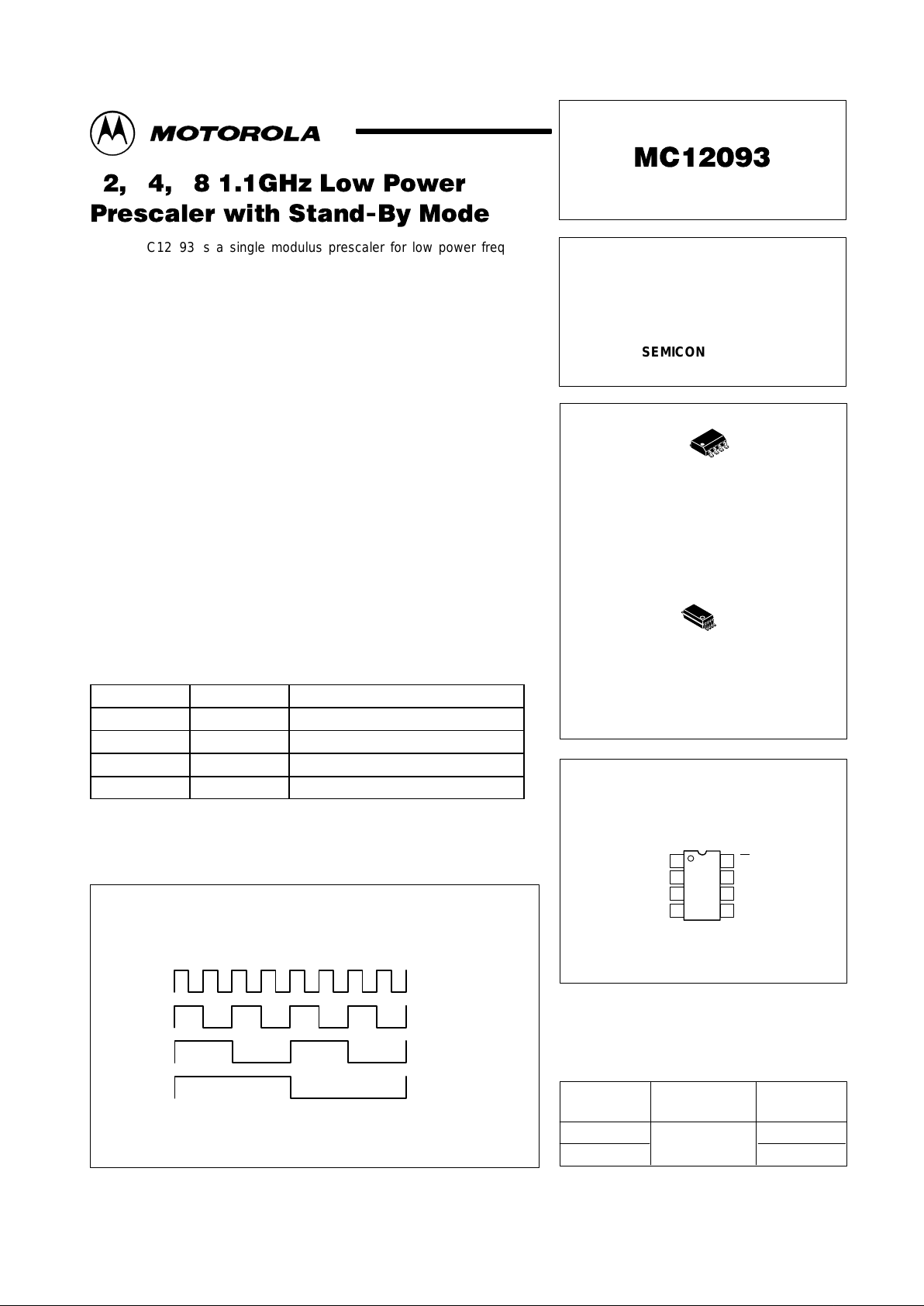
8
1
1
8
IN
(Top View)
8
IN
V
CC
SW2
OUT
SB
SW1
Gnd
7
6
5
1
2
3
4
Device
Operating
Temp Range
Package
ORDERING INFORMATION
MC12093D
MC12093SD
TA =
–40° to +85°C
SO–8
SSOP–8
A LOW on the Stand–By Pin 7 disables the device.
÷
÷ ÷ "
!
The MC12093 is a single modulus prescaler for low power frequency
division of a 1.1 GHz high frequency input signal. Motorola’s advanced
MOSAIC V technology is utilized to acheive low power dissipation of
6.75 mW at a minimum supply voltage of 2.7 V.
On–chip output termination provides output current to drive a 2.0 pF
(typical) high impedance load. If additional drive is required for the prescaler
output, an external resistor can be added parallel from the OUT pin to GND
to increase the output power. Care must be taken not to exceed the
maximum allowable current through the output.
Divide ratio control inputs SW1 and SW2 select the required divide ratio of
÷2, ÷4, or ÷8.
Stand–By mode is featured to reduce current drain to 50 µA typical when
the standby pin SB is switched LOW disabling the prescaler.
• 1.1 GHz Toggle Frequency
• Supply Voltage 2.7 V to 5.5 Vdc
• Low Power 3.0 mA Typical
• Operating Temperature –40 to 85°C
• Divide by 2, 4 or 8 Selected by SW1 and SW2 Pins
• On–Chip Termination
MOSAIC V is a trademark of Motorola
FUNCTIONAL TABLE
SW SW2 Divide Ratio
L L 8
H L 4
L H 4
H H 2
NOTES: 1.SW1 & SW2: H = (VCC – 0.5 V) to VCC; L = Open.
2.SB: H = 2.0 V to VCC, L = GND to 0.8 V.
Motorola, Inc. 1997 Rev 3
IN
÷2
÷4
÷8
Function Chart
MC12093
2
MOTOROLA RF/IF DEVICE DATA
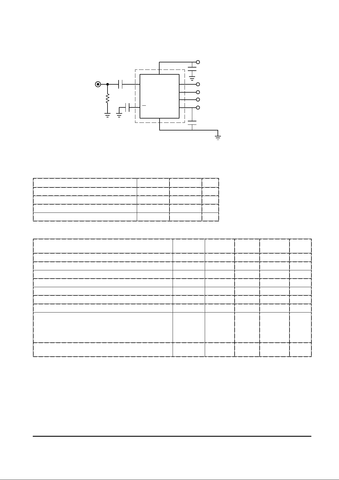
Figure 1. AC Test Circuit
SB
SW1
SW2
OUT
GND
C4
IN
IN
50
Ω
C2
C1
V
CC
C3
EXTERNAL
COMPONENTS
C1 = C2 = 1000 pF
C3 = 0.1
µ
F
C4 = 2.0 pF Load
VCC = 2.7 to 5.5 V
MAXIMUM RATINGS
Parameter
Symbol Value Unit
Power Supply Voltage, Pin 2 V
CC
–0.5 to 6.0 Vdc
Operating Temperature Range T
A
–40 to 85 °C
Storage Temperature Range Tstg –65 to 150 °C
Maximum Output Current, Pin 4 I
O
4.0 mA
NOTE: ESD data available upon request.
ELECTRICAL CHARACTERISTICS (V
CC
= 2.7 to 5.5 V; TA = –40 to 85°C)
Parameter
Symbol Min Typ Max Unit
Toggle Frequency (Sine Wave) ft 0.1 1.4 1.1 GHz
Supply Current I
CC
– 3.0 4.5 mA
Stand–By Current ISB – 120 200 µA
Stand–By Input HIGH (SB) V
IH1
2.0 – V
CC
V
Stand–By Input LOW (SB) V
IL1
Gnd – 0.8 V
Divide Ratio Control Input HIGH (SW1 & SW2) V
IH2
VCC – 0.5 V
CC
VCC + 0.5 V
Divide Ratio Control Input LOW (SW1 & SW2) V
IL2
OPEN OPEN OPEN
Output Voltage Swing (2.0 pF Load)
Output Frequency 12.5–350 MHz (Note 1)
Output Frequency 350–400 MHz (Note 2)
Output Frequency 400–450 MHz (Note 3)
Output Frequency 450–550 MHz (Note 4)
V
OUT
0.6
0.5
0.4
0.3
0.80
0.70
0.55
0.45
–
–
–
–
V
pp
Input Voltage Sensitivity 250–1 100 MHz
100–250 MHz
V
IN
100
400
–
–
1000
1000
mVpp
NOTES: 1.Input frequency 1.1 GHz, ÷8, minimum output frequency of 12.5 MHz.
2.Input frequency 700–800 MHz, ÷2.
3.Input frequency 800–900 MHz, ÷2.
4.Input frequency 900–1100 MHz, ÷2.
 Loading...