

Motorola MC12089D, MC12089P Datasheet
SEMICONDUCTOR
TECHNICAL DATA
MECL PLL COMPONENTS
÷64/128 PRESCALER
Order this document by MC12089/D
P SUFFIX
PLASTIC PACKAGE
CASE 626
PIN CONNECTIONS
D SUFFIX
PLASTIC PACKAGE
CASE 751
(SO–8)
8
1
1
8
NC
(Top View)
8
Gnd
IN
IN
V
CC
OUT
NC
SW
7
6
5
1
2
3
4
Device
Operating
Temperature Range
Package
ORDERING INFORMATION
MC12089D
MC12089P
TA = – 40° to +85°C
SO–8
Plastic
The MC12089 is a single modulus divide by 64 and 128 prescaler for low
power frequency division of a 2.8 GHz high frequency input signal. The low
power (10.2 mA typical at 5.0 V) and high operating frequency features make
this prescaler ideal in satellite TV receiver applications.
Divide ratio control input SW selects the required divide ratio of ÷64 or
÷128.
On–chip output termination provides 2.5 mA of output current to drive a
12 pF (typical) high impedance load. The output voltage swing under typical
supply voltage and temperature conditions is 1.2 V. If additional drive is
required for the prescaler output, an external resistor can be added in
parallel from the OUT pin to Gnd to increase the output power. Care must be
taken not to exceed the maximum allowable current through the output.
• 2.8 GHz Toggle Frequency
• Supply Voltage 4.5 to 5.5 V
• Low Power Dissipation 51 mW Typical
• Operating Temperature Range of –40 to 85°C
FUNCTIONAL TABLE
SW Divide Ratio
H 64
L 128
NOTE: H = VCC, L = Open.
MAXIMUM RATINGS
Characteristic Symbol Range Unit
Power Supply Voltage, Pin 4 V
CC
–0.5 to 7.0 Vdc
Operating Temperature Range T
A
–40 to 85 °C
Storage Temperature Range T
stg
–65 to 150 °C
Maximum Output Current, Pin 7 I
O
4.0 mA
NOTE: ESD data available upon request.
Motorola, Inc. 1997 Rev 3
MC12089
2
MOTOROLA RF/IF DEVICE DATA
ELECTRICAL CHARACTERISTICS
(VCC = 4.5 to 5.5 V; TA = –40 to 85°C, unless otherwise noted.)
Parameter
Symbol Min Typ Max Unit
Toggle Frequency (Sine Wave) ft 0.25 3.4 2.8 GHz
Supply Current Output (Pin 2) I
CC
– 10.2 14.5 mA
Input Voltage Sensitivity 250–500 MHz
500–2800 MHz
V
in
400
100
–
–
1000
1000
mVpp
Divide Ratio Control Input High (SW) V
IH
V
CC
V
CC
V
CC
V
Divide Ratio Control Input Low (SW) V
IL
Open Open Open –
Output Voltage Swing (Note 1) V
out
0.8 1.2 – V
pp
NOTE: 1.Assumes CL = 12 pF
DQB
CQ
DQ
CQB
DQB
C
Q
In
In
Out
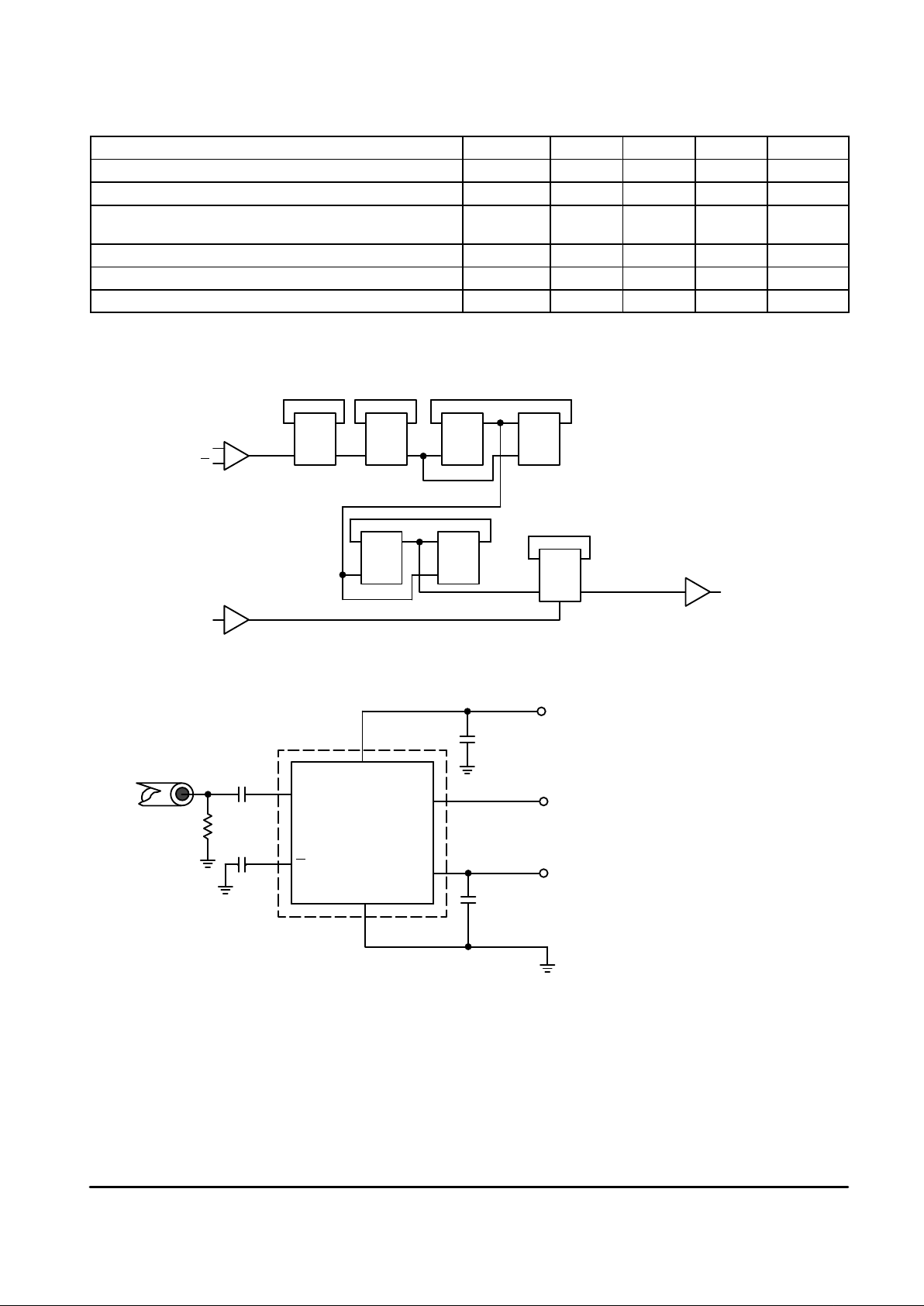
Figure 1. Logic Diagram (MC12089)
DQ
CQB
DQB
C
Q
DQB
CQ
SW
DQB
CQ
Figure 2. AC Test Circuit
SINE WAVE GENERATOR
50
Ω
C1
C2
C3
VCC = 4.5 to 5.5 V
C
L
V
CC
IN
IN
GND
OUT
EXTERNAL COMPONENTS
C1 = C2 = 1000 pF
C3 = 0.1
µ
F
CL = 12 pF (Including Scope and Jig Capacitance)
SW
 Loading...