

MOTOROLA MC10H123FNR2, MC10H123M Datasheet
SEMICONDUCTOR TECHNICAL DATA
2–41
REV 5
Motorola, Inc. 1996
3/93
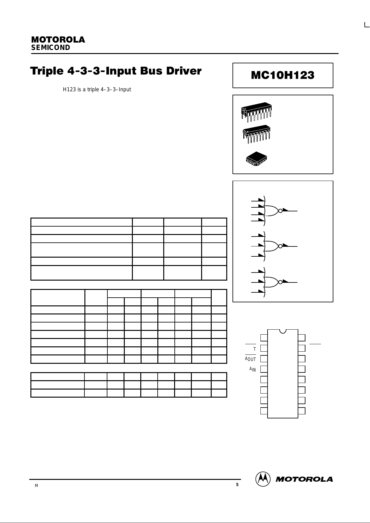
The MC10H123 is a triple 4–3–3–Input Bus Driver.
The MC10H123 consists of three NOR gates designed for bus driving
applications on card or between cards. Output low logic levels are specified with
VOL = –2.1 Vdc so that the bus may be terminated to –2.0 Vdc. The gate output,
when low, appears as a high impedance to the bus, because the output
emitter–followers of the MC10H123 are “turned–off.” This eliminates
discontinuities in the characteristic impedance of the bus.
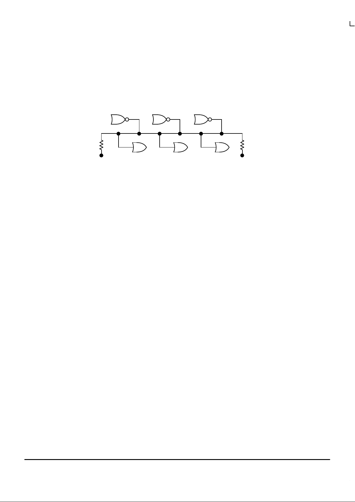
The VOH level is specified when driving a 25–ohm load terminated to –2.0
Vdc, the equivalent of a 50–ohm bus terminated at both ends. Although 25
ohms is the lowest characteristic impedance that can be driven by the
MC10H123, higher impedance values may be used with this part. A typical
50–ohm bus is shown in Figure 1.
• Propagation Delay, 1.5 ns Typical
• Improved Noise Margin 150 mV (Over Operating Voltage and
Temperature Range)
• Voltage Compensated
• MECL 10K–Compatible
MAXIMUM RATINGS
Characteristic Symbol Rating Unit
Power Supply (VCC = 0) V
EE
–8.0 to 0 Vdc
Input Voltage (VCC = 0) V
I
0 to V
EE
Vdc
Output Current— Continuous
— Surge
I
out
50
100
mA
Operating Temperature Range T
A
0 to +75 °C
Storage Temperature Range— Plastic
— Ceramic
T
stg
–55 to +150
–55 to +165
°C
°C
ELECTRICAL CHARACTERISTICS (VEE = –5.2 V ±5%) (See Note)
0° 25° 75°
Characteristic Symbol Min Max Min Max Min Max Unit
Power Supply Current I
E
— 60 — 56 — 60 mA
Input Current High I
inH
— 495 — 310 — 310 µA
Input Current Low I
inL
0.5 — 0.5 — 0.3 — µA
High Output Voltage V
OH
–1.02 –0.84 –0.98 –0.81 –0.92 –0.735 Vdc
Low Output Voltage V
OL
–2.1 –2.03 –2.1 –2.03 –2.1 –2.03 Vdc
High Input Voltage V
IH
–1.17 –0.84 –1.13 –0.81 –1.07 –0.735 Vdc
Low Input Voltage V
IL
–1.95 –1.48 –1.95 –1.48 –1.95 –1.45 Vdc
AC PARAMETERS
Propagation Delay t
pd
0.7 1.5 0.7 1.6 0.7 1.7 ns
Rise Time t
r
0.7 1.6 0.7 1.7 0.7 1.8 ns
Fall Time t
f
0.7 1.6 0.7 1.7 0.7 1.8 ns
NOTE:
Each MECL 10H series circuit has been designed to meet the dc specifications shown in the test table,
after thermal equilibrium has been established. The circuit is in a test socket or mounted on a printed circuit
board and transverse air flow greater than 500 Ifpm is maintained. Outputs are terminated through a
50–ohm resistor to –2.1 volts.
LOGIC DIAGRAM
DIP
PIN ASSIGNMENT
V
CC1
B
OUT
A
OUT
A
IN
A
IN
A
IN
A
IN
V
EE
V
CC2
C
OUT
C
IN
C
IN
C
IN
B
IN
B
IN
B
IN
16
15
14
13
12
11
10
9
1
2
3
4
5
6
7
8
V
CC1
= PIN 1
V
CC2
= PIN 16
VEE = PIN 8
3
5
6
7
4
2
9
10
11
15
12
13
14
L SUFFIX
CERAMIC PACKAGE
CASE 620–10
P SUFFIX
PLASTIC PACKAGE
CASE 648–08
FN SUFFIX
PLCC
CASE 775–02
Pin assignment is for Dual–in–Line Package.
For PLCC pin assignment, see the Pin Conversion
T ables on page 6–11 of the Motorola MECL Data
Book (DL122/D).
MC10H123
MOTOROLA MECL Data
DL122 — Rev 6
2–42
FIGURE 1 — 50–OHM BUS DRIVER (25–OHM LOAD)
1/3 MC10H123
1/3 MC10H123 1/3 MC10H123
ZO = 50
Ω
–2.0
VDC
RECEIVERS (MECL GATES)
–2.0
VDC
50
Ω
50
Ω
 Loading...