

Motorola MC10124FN, MC10124L, MC10124P Datasheet
SEMICONDUCTOR TECHNICAL DATA
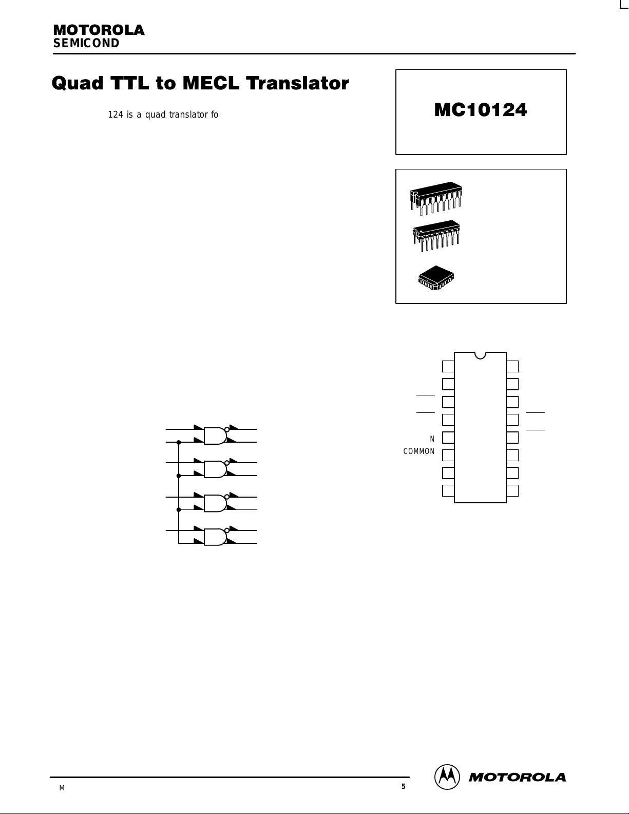
The MC10124 is a quad translator for interfacing data and control signals
between a saturated logic section and the MECL section of digital systems. The
MC10124 has TTL compatible inputs, and MECL complementary open–emitter
outputs that allow use as an inverting/ non–inverting translator or as a
differential line driver . When the common strobe input is at the low logic level, it
forces all true outputs to a MECL low logic state and all inverting outputs to a
MECL high logic state.
Power supply requirements are ground, +5.0 Volts, and –5.2 Volts.
Propagation delay of the MC10124 is typically 3.5 ns. The dc levels are
standard or Schottky TTL in, MECL 10,000 out.
An advantage of this device is that TTL level information can be transmitted
differentially , via balanced twisted pair lines, to the MECL equipment, where the
signal can be received by the MC10115 or MC10116 differential line receivers.
The MC10124 is useful in computers, instrumentation, peripheral controllers,
test equipment, and digital communications systems.
PD= 380 mW typ/pkg (No Load)
tpd= 3.5 ns typ (+ 1.5 Vdc in to 50% out)
tr, tf= 2.5 ns typ (20%–80%)
LOGIC DIAGRAM
5
6
7
10
11
4
2
3
1
12
15
13
14
L SUFFIX
CERAMIC PACKAGE
CASE 620–10
P SUFFIX
PLASTIC PACKAGE
CASE 648–08
FN SUFFIX
PLCC
CASE 775–02
DIP
PIN ASSIGNMENT
B
OUT
A
OUT
B
OUT
A
OUT
A
IN
COMMON
STROBE
B
IN
V
EE
Pin assignment is for Dual–in–Line Package.
For PLCC pin assignment, see the Pin Conversion
T ables on page 6–11 of the Motorola MECL Data
1
2
3
4
5
6
7
8
Book (DL122/D).
16
15
14
13
12
11
10
GND
C
OUT
D
OUT
D
OUT
C
OUT
D
IN
C
IN
V
9
CC
3/93
Motorola, Inc. 1996
Gnd = PIN 16
VCC (+5.0Vdc) = PIN 9
VEE (–5.2Vdc) = PIN 8
3–82
REV 5
MC10124
Under
pp y
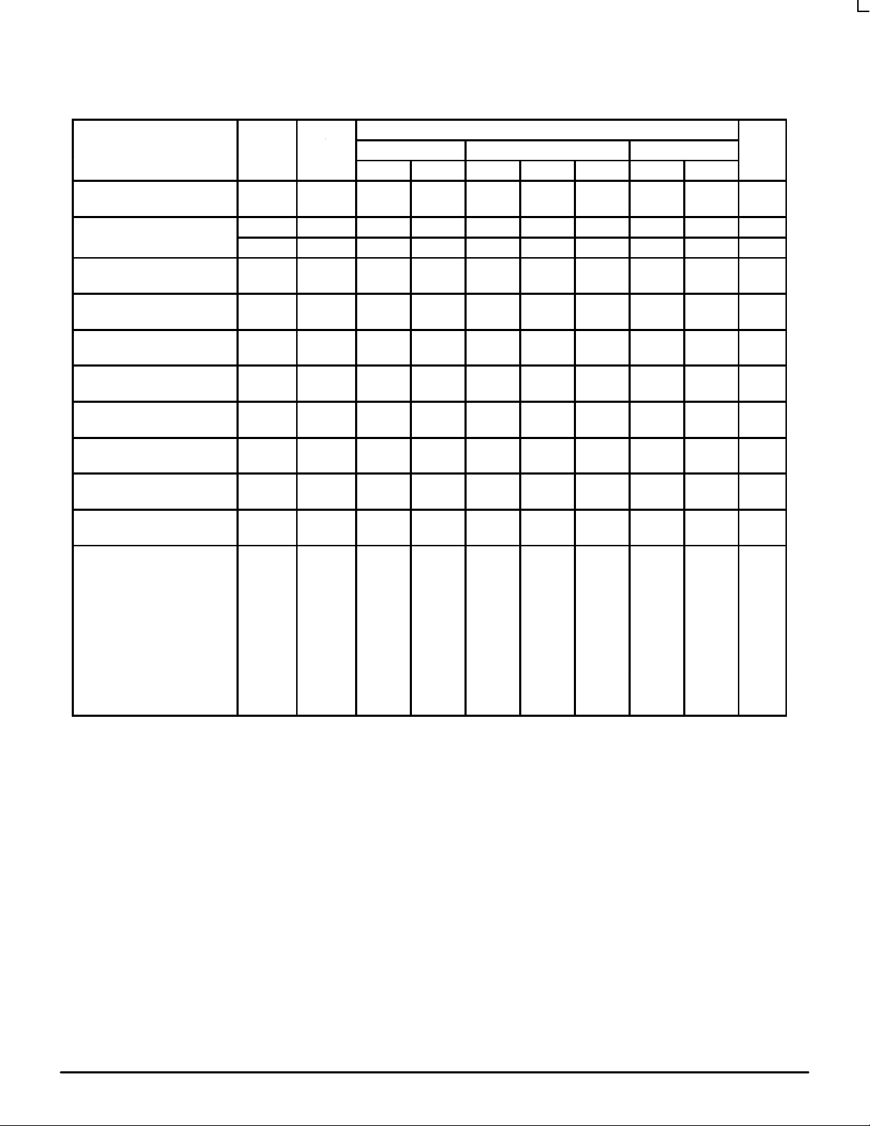
ELECTRICAL CHARACTERISTICS
Test Limits
Pin
Characteristic Symbol
Negative Power Supply Drain
Current
Positive Power Supply Drain
Current
Reverse Current I
Forward Current I
Input Breakdown Voltage BV
Clamp Input Voltage V
High Output Voltage V
Low Output Voltage V
High Threshold Voltage V
Low Threshold Voltage V
Switching Times (50Ω Load) ns
Propagation Delay
(+3.5Vdc to 50%)
I
E
I
CCH
I
CCL
R
F
OH
OL
OHA
OLA
t
6+1+
1
t
6–1–
t
7+1+
t
7–1–
t
7+3–
t
7–3+
Under
Test
8 72 66 72 mAdc
9 16 16 18 mAdc
9 25 25 25 mAdc
6
7
6
7
in
I
6
7
6
7
1
3
1
3
1
3
1
3
1
1
1
1
3
3
–30°C +25°C +85°C
Min Max Min Typ Max Min Max
5.5
5.5
–1.060
–1.060
–1.890
–1.890
–1.080
–1.080
1.5
1.0
1.5
1.0
1.5
1.0
200
50
–12.8
–3.2
–1.5
–1.5
–0.890
–0.890
–1.675
–1.675
–1.655
–1.655
6.8
6.0
6.8
6.0
6.8
6.0
5.5
5.5
–0.960
–0.960
–1.850
–1.850
–0.980
–0.980
1.0
1.0
1.0
1.0
1.0
1.0
3.5
3.5
3.5
3.5
3.5
3.5
200
50
–12.8
–3.2
–1.5
–1.5
–0.810
–0.810
–1.650
–1.650
–1.630
–1.630
6.0
6.0
6.0
6.0
6.0
6.0
5.5
5.5
–0.890
–0.890
–1.825
–1.825
–0.910
–0.910
1.0
1.5
1.0
1.5
1.0
1.5
–0.700
–0.700
–1.615
–1.615
–1.595
–1.595
20050µAdc
–12.8
–3.2
–1.5
–1.5
6.0
6.8
6.0
6.8
6.0
6.8
Unit
mAdc
Vdc
Vdc
Vdc
Vdc
Vdc
Vdc
Rise Time (20 to 80%) t
Fall Time (20 to 80%) t
1. See switching time test circuit. Propagation delay for this circuit is specified from +1.5Vdc in to the 50% point on the output waveform. The
+3.5Vdc is shown here because all logic and supply levels are shifted 2 volts positive.
DL122 — Rev 6
1+
1–
1 1.0 4.2 1.1 2.5 3.9 1.1 4.3
1 1.0 4.2 1.1 2.5 3.9 1.1 4.3
3–83 MOTOROLAMECL Data

MC10124
Und
pp y
ELECTRICAL CHARACTERISTICS (continued)
TEST VOLTAGE VALUES (Volts)
@ Test Temperature V
–30°C +4.0 +0.40 +2.00 +1.10 +0.40
+25°C +4.0 +0.40 +1.80 +1.10 +0.40
+85°C +4.0 +0.40 +1.80 +0.90 +0.40
Pin
Characteristic Symbol
Negative Power Supply Drain
Current
Positive Power Supply Drain
Current
Reverse Current I
Forward Current I
Input Breakdown Voltage BV
Clamp Input Voltage V
High Output Voltage V
Low Output Voltage V
High Threshold Voltage V
Low Threshold Voltage V
Switching Times (50Ω Load) +6.0 V Pulse In Pulse Out +2.0 V
Propagation Delay
(+3.5Vdc to 50%)
Rise Time (20 to 80%) t
Fall Time (20 to 80%) t
1. See switching time test circuit. Propagation delay for this circuit is specified from +1.5Vdc in to the 50% point on the output waveform. The
+3.5Vdc is shown here because all logic and supply levels are shifted 2 volts positive.
I
E
I
CCH
I
CCL
R
F
in
I
OH
OL
OHA
OLA
t
6+1+
1
t
6–1–
t
7+1+
t
7–1–
t
7+3–
t
7–3+
1+
1–
er
Test
8 16
9 5,6,7,10,11 16
9
6
7
6
7
6
7
6
7
1
3
1
3
1
3
1
3
1
1
1
1
3
3
1 6 7 1 16
1 6 7 1 16
IH
TEST VOLTAGE APPLIED TO PINS LISTED BELOW
V
IH
5,7,10,1 1
6
6,7
6,7
6
6
6
6
7
7
6
6
6
6
V
ILmax
V
ILmax
6,7
6,7 16
6
6
7
7
7
7
V
V
IHA’
IHA’
7
7
1
1
1
1
3
3
V
ILA’
V
ILA’
7
7 16
V
F
V
F
5,7,10,1 1
6
6
7
5,6,7,10,11,16
5,7,10,1 1,16
Gnd
16
16
16
16
6,16
16
16
16
16
16
16
16
16
16
16
16
16
16
16
MOTOROLA MECL Data
3–84
DL122 — Rev 6
 Loading...