

MOTOROLA MC10123FNR2 Datasheet

SEMICONDUCTOR TECHNICAL DATA
3–78
REV 5
Motorola, Inc. 1996
3/93
The MC10123 consists of three NOR gates designed for bus driving
applications on card or between cards. Output low logic levels are specified with
VOL = –2.1 Vdc so that the bus may be terminated to –2.0 Vdc. The gate output,
when low, appears as a high impedance to the bus, because the output emitter–
followers of the MC10123 are “turned–off.” This eliminates discontinuities in the
characteristic impedance of the bus.
The VOH level is specified when driving a 25–ohm load terminated to –2.0
Vdc, the equivalent of a 50–ohm bus terminated at both ends. Although 25
ohms is the lowest characteristic impedance that can be driven by the
MC10123, higher impedance values may be used with this part. A typical
50–ohm bus is shown in Figure 1.
PD= 310 mW typ/pkg (No Load)
tpd= 3.0 ns typ
tr, tf= 2.5 ns typ (20%–80%)
LOGIC DIAGRAM
V
CC1
= PIN 1
V
CC2
= PIN 16
VEE= PIN 8
14
12
13
15
11
9
10
2
7
5
3
6
4
FIGURE 1 — 50–OHM BUS DRIVER (TYPICAL APPLICATION)
1/3 MC10123
1/3 MC10123 1/3 MC10123
ZO = 50
Ω
–2.0
VDC
RECEIVERS (MECL GATES)
–2.0
VDC
50
Ω
50
Ω
DIP
PIN ASSIGNMENT
V
CC1
B
OUT
A
OUT
A
IN
A
IN
A
IN
A
IN
V
EE
V
CC2
C
OUT
C
IN
C
IN
C
IN
B
IN
B
IN
B
IN
16
15
14
13
12
11
10
9
1
2
3
4
5
6
7
8
L SUFFIX
CERAMIC PACKAGE
CASE 620–10
P SUFFIX
PLASTIC PACKAGE
CASE 648–08
FN SUFFIX
PLCC
CASE 775–02
Pin assignment is for Dual–in–Line Package.
For PLCC pin assignment, see the Pin Conversion
T ables on page 6–11 of the Motorola MECL Data
Book (DL122/D).
MC10123
3–79 MOTOROLAMECL Data
DL122 — Rev 6
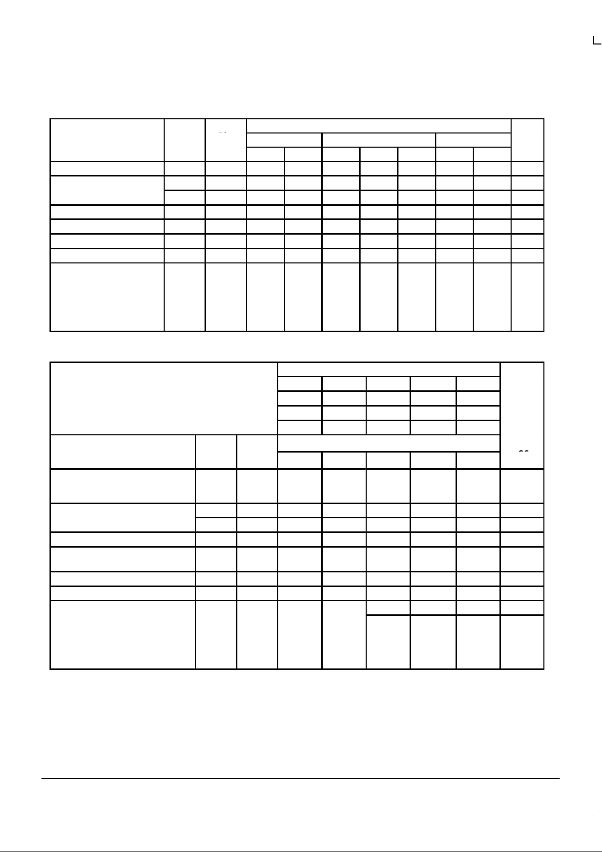
ELECTRICAL CHARACTERISTICS
Test Limits
Pin
Under
–30°C +25°C +85°C
Characteristic Symbol
Under
Test
Min Max Min Typ Max Min Max
Unit
Power Supply Drain Current I
E
8 82 71 75 82 mAdc
Input Current I
inH
4 350 220 220 µAdc
I
inL
4 0.5 µAdc
Output Voltage Logic 1 V
OH
3 –1.060 –0.890 –0.960 –0.810 –0.890 –0.700 Vdc
Output Voltage Logic 0 V
OL
3 –2.100 –2.030 –2.100 –2.030 –2.100 –2.030 Vdc
Threshold Voltage Logic 1 V
OHA
3 –1.080 –0.980 –0.910 Vdc
Threshold Voltage Logic 0 V
OLA
3 –2.100 –2.100 –2.100 Vdc
Switching Times (50Ω Load) ns
Propagation Delay t
4+3–
t
4–3+
3
3
1.2
1.2
4.6
4.6
1.2
1.2
3.0
3.0
4.4
4.4
1.2
1.2
4.8
4.8
Rise Time (20 to 80%) t
3+
3 1.0 3.7 1.0 2.5 3.5 1.0 3.9
Fall Time (20 to 80%) t
3–
3 1.0 3.7 1.0 2.5 3.5 1.0 3.9
ELECTRICAL CHARACTERISTICS (continued)
TEST VOLTAGE VALUES (Volts)
@ Test Temperature V
IHmax
V
ILmin
V
IHAminVILAmax
V
EE
–30°C –0.890 –1.890 –1.205 –1.500 –5.2
+25°C –0.810 –1.850 –1.105 –1.475 –5.2
+85°C –0.700 –1.825 –1.035 –1.440 –5.2
Pin
TEST VOLTAGE APPLIED TO PINS LISTED BELOW
Characteristic Symbol
Und
er
Test
V
IHmax
V
ILmin
V
IHAminVILAmax
V
EE
(VCC)
Gnd
Power Supply Drain Current I
E
8 4,5,6,7,9
10,11,12
13,14
8 1, 16
Input Current I
inH
4 4 8 1, 16
I
inL
4 4 8 1, 16
Output Voltage Logic 1 V
OH
3 8 1, 16
Output Voltage Logic 0 V
OL
3 4,5,6,7
9,12
8 1, 16
Threshold Voltage Logic 1 V
OHA
3 4,5,6,7 8 1, 16
Threshold Voltage Logic 0 V
OLA
3 9,12 4,5,6,7 8 1, 16
Switching Times (50Ω Load) Pulse In Pulse Out –3.2 V +2.0 V
Propagation Delay t
4+3–
t
4–3+
3
3
4
4
3
3
8
8
1, 16
1, 16
Rise Time (20 to 80%) t
3+
3 4 3 8 1, 16
Fall Time (20 to 80%) t
3–
3 4 3 8 1, 16
Each MECL 10,000 series circuit has been designed to meet the dc specifications shown in the test table, after thermal equilibrium has been
established. The circuit is in a test socket or mounted on a printed circuit board and transverse air flow greater than 500 linear fpm is maintained.
Outputs are terminated through a 50-ohm resistor to –2.0 volts. Test procedures are shown for only one gate. The other gates are tested in the
same manner.
 Loading...