

Motorola MC100EP221 Datasheet

SEMICONDUCTOR TECHNICAL DATA
1
REV 0.1
Motorola, Inc. 1997
2/97
The MC100EP221 is a low skew 1–to–20 differential driver, designed
with clock distribution in mind. It accepts two clock sources into an input
multiplexer. The input signals can be either differential or single–ended if
the VBB output is used. The selected signal is fanned out to 20 identical
differential outputs.
• 150ps Part–to–Part Skew
• 50ps Output–to–Output Skew
• Differential Design
• V
BB
Output
• Voltage and Temperature Compensated Outputs
• Low Voltage V
EE
Range of –2.375 to –3.8V
• 75kΩ Input Pulldown Resistors
The EP221 is specifically designed, modeled and produced with low
skew as the key goal. Optimal design and layout serve to minimize gate–
to–gate skew within a device, and empirical modeling is used to
determine process control limits that ensure consistent tpd distributions
from lot to lot. The net result is a dependable, guaranteed low skew
device.
To ensure that the tight skew specification is met it is necessary that
both sides of the differential output are terminated into 50Ω, even if only
one side is being used. In most applications, all ten differential pairs will
be used and therefore terminated. In the case where fewer than ten pairs
are used, it is necessary to terminate at least the output pairs on the same
package side as the pair(s) being used on that side, in order to maintain
minimum skew. Failure to do this will result in small degradations of
propagation delay (on the order of 10–20ps) of the output(s) being used
which, while not being catastrophic to most designs, will mean a loss of
skew margin.
The MC100EP221, as with most other ECL devices, can be operated from a positive VCC supply in PECL mode. This allows
the EP221 to be used for high performance clock distribution in +3.3V or +2.5V systems. Designers can take advantage of the
EP221’s performance to distribute low skew clocks across the backplane. In a PECL environment, series or Thevenin line
terminations are typically used as they require no additional power supplies. For more information on using PECL, designers
should refer to Motorola Application Note AN1406/D.
This document contains information on a product under development. Motorola reserves the right to change or
discontinue this product without notice.
LOW–VOL TAGE
1:20 DIFFERENTIAL
ECL/PECL CLOCK DRIVER
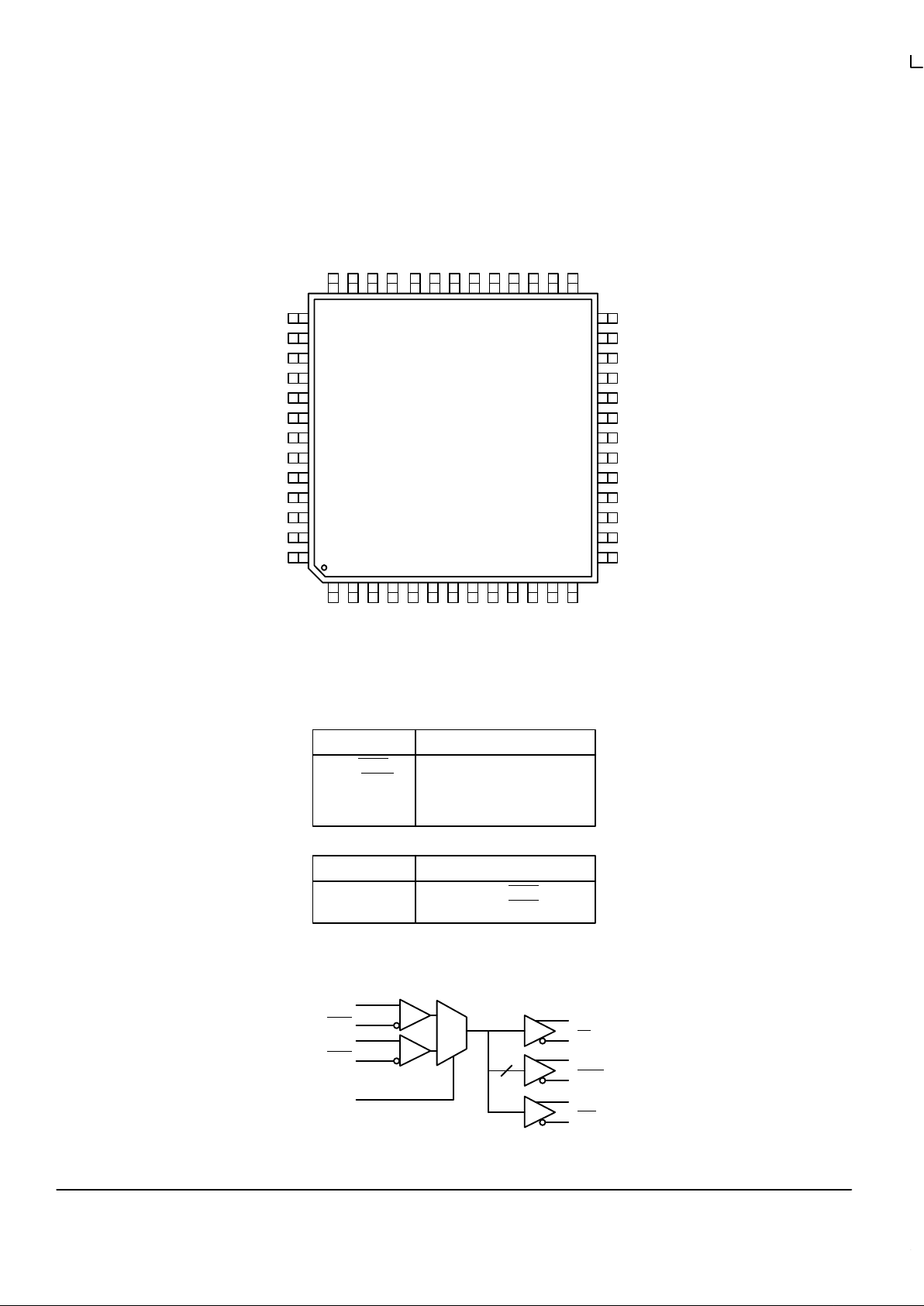
FA SUFFIX
52–LEAD TQFP PACKAGE
CASE 848D–03
MC100EP221
MOTOROLA TIMING SOLUTIONS
BR1333 — Rev 6
2
PIN NAMES
Function
Differential Input Pairs
Differential Outputs
Active Clock Select Input
VBB Output
Pins
CLKn, CLKn
Q0:19, Q0:19
CLK_SEL
VBB
FUNCTION
Active Input
CLK0, CLK0
CLK1, CLK1
CLK_SEL
0
1
LOGIC SYMBOL
Q0
Q0
0
1
CLK0
CLK0
CLK1
CLK1
CLK_SEL
Pinout: 52–Lead TQFP
(Top View)
Q1:18
Q1:18
Q19
Q19
16
VCCO
Q5B
Q5
Q4B
Q4
Q3B
Q3
Q2B
Q2
Q1B
Q1
Q0B
Q0
Q12
Q12B
Q13
Q13B
Q14
Q14B
Q15
Q15B
Q16
Q16B
Q17
Q17B
VCCO
Q6
Q6BQ7Q7BQ8Q8BQ9Q9B
Q10
Q10B
Q11
Q11B
VCCO
VCC
VCCO
CLKSEL
CLK0
CLK0B
VBB
CLK1
CLK1B
VEE
Q19B
Q19
Q18B
Q18
40
41
42
43
44
45
46
47
48
49
50
51
52
25
24
23
22
21
20
19
18
17
16
15
14
12345678910111213
39 38 37 36 35 34 33 32 31 30 29 28 27
26
MC100EP211
 Loading...