

MOTOROLA MC10ELT25D, MC10ELT25DR2, MC100ELT25DR2, MC100ELT25D Datasheet
MC10ELT25, MC100ELT25
Differential ECL to TTL
Translator
The MC10ELT/100ELT25 is a differential ECL to TTL translator.
Because ECL levels are used a +5V, -5.2V (or -4.5V) and ground are
required. The small outline 8-lead SOIC package and the single gate of
the ELT25 makes it ideal for those applications where space,
performance and low power are at a premium. Because the mature
MOSAIC 1.5 process is used, low cost can be added to the list of
features.
The VBB output allows the EL T25 to also be used in a single-ended
input mode. In this mode the VBB output is tied to the IN
non-inverting buffer or the IN input for an inverting buffer. If used the
VBB pin should be bypassed to ground via a 0.01µF capacitor.
The ELT25 is available in both ECL standards: the 10ELT is
compatible with MECL 10H logic levels while the 100ELT is
compatible with ECL 100K logic levels. For further information
regarding modeling, refer to AN1596/D “ECLinPS Lite Translator
ELT Family SPICE I/O Model Kit”.
• 2.6ns Typical Propagation Delay
• Internal Input Resistors: Pulldown on D, Pulldown and Pullup on D
• Q Output will default LOW with inputs open or at V
• Differential ECL Inputs
• Small Outline SOIC Package
• 24mA TTL Outputs
• Flow Through Pinouts
• Moisture Sensitivity Level 1, Indefinite Time Out of Drypack.
For Additional Information, See Application Note AND8003/D
• Flammability Rating: UL–94 code V–0 @ 1/8”,
Oxygen Index 28 to 34
• Transistor Count: 135 devices
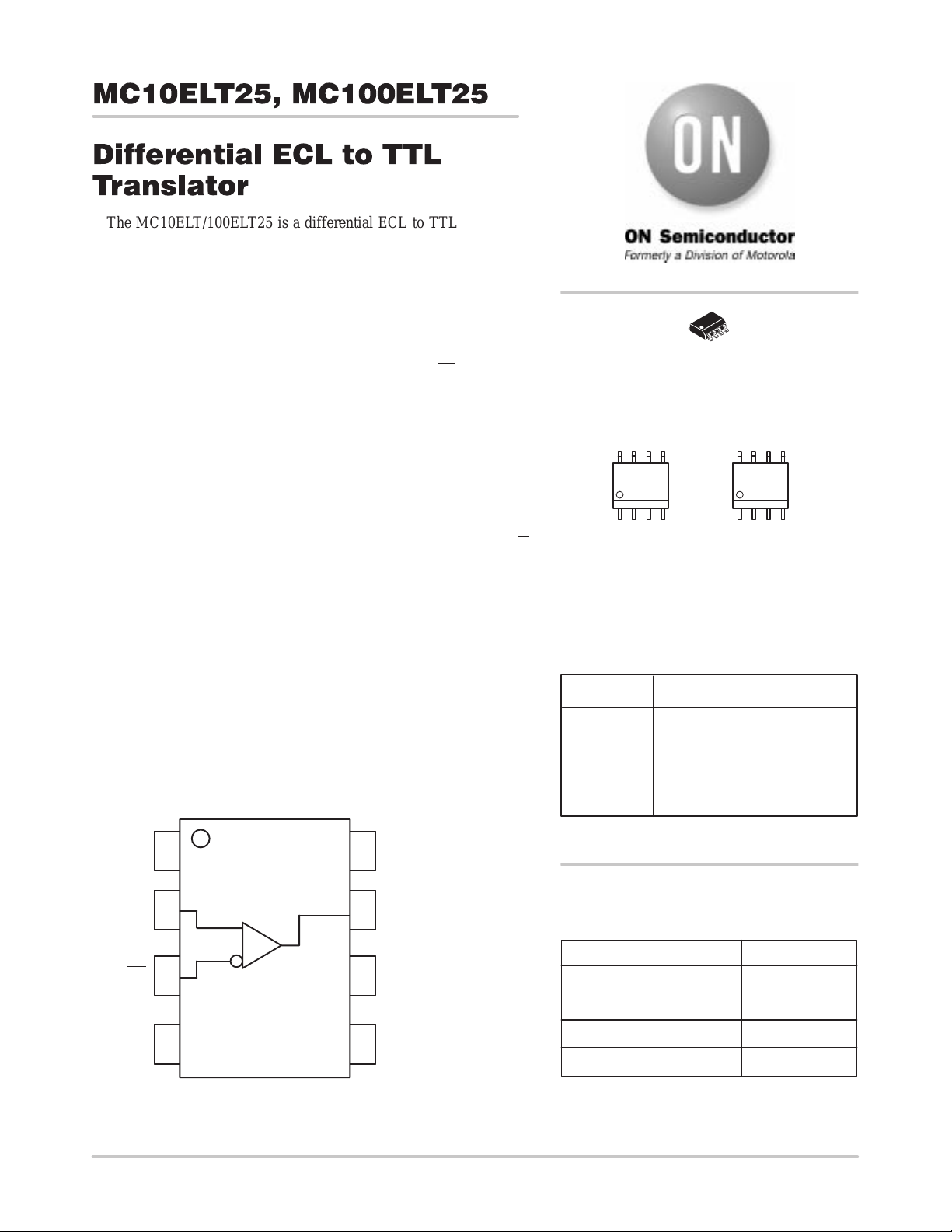
LOGIC DIAGRAM AND PINOUT ASSIGNMENT
input for a
EE
http://onsemi.com
8
1
SO–8
D SUFFIX
CASE 751
MARKING DIAGRAM
8
HLT25
ALYW
1
H = MC10
K = MC100
A = Assembly Location
*For additional information, see Application Note
AND8002/D
PIN DESCRIPTION
PIN FUNCTION
D Diff ECL Inputs
Q TTL Output
V
CC
V
EE
V
BB
GND Ground
Positive Supply
Negative Supply
Reference Output
8
KLT25
ALYW
1
L = Wafer Lot
Y = Year
W = Work Week
1
V
EE
2
D0
ECL
3
V
Semiconductor Components Industries, LLC, 1999
February , 2000 – Rev. 3
45
BB
TTL
V
78Q0
6
NCD0
GND
CC
ORDERING INFORMATION
Device Package Shipping
MC10EL T25D SO–8 98 Units / Rail
MC10EL T25DR2 SO–8
MC100EL T25D SO–8 98 Units / Rail
MC100EL T25DR2 SO–8
1 Publication Order Number:
2500 Units / Reel
2500 Units / Reel
MC10ELT25/D
MC10ELT25, MC100ELT25
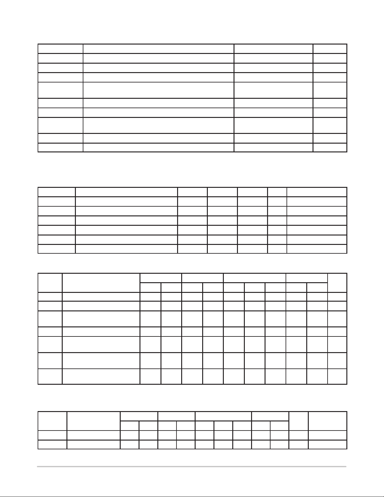
MAXIMUM RATINGS*
Symbol Parameter Value Unit
V
CC
V
EE
V
IN
I
OUT
T
A
T
STG
θ
JA
θ
JC
T
sol
* Maximum Ratings are those values beyond which damage to the device may occur. Functional operation should be restricted to the
Recommended Operating Conditions.
TTL OUTPUT DC CHARACTERISTICS
(VCC = 4.5V to 5.5V; VEE = –4.2V to –5.5V 100EL T, –4.94V to –5.5V 10ELT; TA = –40°C to 85°C)
Symbol Characteristic Min Typ Max Unit Condition
V
OH
V
OL
I
CCH
I
CCL
I
EE
I
OS
ECL INPUT DC CHARACTERISTICS
(VCC = 4.5V to 5.5V; VEE = –4.2V to –5.5V 100EL T, –4.94V to –5.5V 10ELT; TA = –40°C to 85°C)
Symbol Characteristic Min Max Min Max Min Typ Max Min Max Unit
I
IH
I
IL
V
CMR
V
PP
V
IH
V
IL
V
BB
1. 200mV input guarantees full logic swing at the output.
Input HIGH Current 150 150 150 150 µA
Input LOW Current 0.5 0.5 0.5 0.5 µA
Common Mode Range VEE +
Minimum Peak-to-Peak Input
Input HIGH Voltage 10ELT
Input LOW Voltage 10EL T
Reference Output 10ELT
DC Supply Voltage (Referenced to GND, VEE = –5.2) 7.0 V
DC Supply Voltage (Referenced to GND, VCC = 5.0) –8.0 V
Input Voltage 0 to V
Current Applied to Output in Low Output State Continuous
Operating Temperature Range (In Free-Air) –40 to 85 °C
Storage Temperature Range –55 to +150 °C
Thermal Resistance (Junction–to–Ambient) Still Air
Thermal Resistance (Junction–to–Case) 41 to 44 ± 5% °C/W
Solder Temperature (<2 to 3 Seconds: 245°C desired) 265 °C
Output HIGH Voltage 2.4 V IOH = –3.0mA
Output LOW Voltage 0.5 V IOL = 24mA
Power Supply Current 11 16 mA
Power Supply Current 13 18 mA
Power Supply Current 15 21 mA
Output Short Circuit Current –150 –60 mA
–40°C 0°C 25°C 85°C
1
100EL T
100EL T
100EL T
V
2.2
200 200 200 200 mV
–1230
–1165
–1950
–1810
–1.43
–1.38
CCVEE
–890
–880
–1500
–1475
–1.30
–1.26
+
2.2
–1170
–1165
–1950
–1810
–1.38
–1.38
Surge
500lfpm
V
CCVEE
–840
–880
–1480
–1475
–1.27
–1.26
+
2.2
–1130
–1165
–1950
–1810
–1.35
–1.38
CC
50
100
190
130
V
CCVEE
–810
–880
–1480
–1475
–1.25
–1.26
2.2
–1060
–1165
–1950
–1810
–1.31
–1.38
+
V
CC
–720
–880
–1445
–1475
–1.19
–1.26
V
mA
°C/W
V
mV
mV
V
AC CHARACTERISTICS
(VCC = 4.5V to 5.5V; VEE = –4.2V to –5.5V 100EL T, –4.94V to –5.5V 10ELT; TA = –40°C to 85°C)
–40°C 0°C 25°C 85°C
Symbol Characteristic Min Max Min Max Min Typ Max Min Max Unit Condition
t
PLH
t
PHL
Propagation Delay 1.7 3.6 1.7 3.6 1.7 3.6 1.7 3.6 ns CL = 20pF
Propagation Delay 2.6 4.1 2.6 4.1 2.6 4.1 2.6 4.1 ns CL = 20pF
http://onsemi.com
2
 Loading...