

SEMICONDUCTOR TECHNICAL DATA
4–1
REV 1
Motorola, Inc. 1996
7/95
The MC100LVEL/EL90 is a triple ECL to PECL translator. The device
receives either standard or low voltage differential ECL signals and
translates them to either standard or low voltage differential PECL output
signals. The L VEL device can handle the low voltage signals while the EL
device is designed for the standard signals. It is possible to have low
voltage signals on one side and standard signals on the other if the
LVEL90 is used.
• 500ps Propagation Delays
• Fully Differential Design
• Supports both Standard and Low Voltage Operation
• 20–Lead SOIC Packaging
A VBB output is provided for interfacing with single ended ECL signals
at the input. If a single ended input is to be used the VBB output should be
connected to the D
input. The active signal would then drive the D input.
When used the VBB output should be bypassed to ground via a 0.01µF
capacitor. The VBB output is designed to act as the switching reference
for the EL90 under single ended input switching conditions, as a result
this pin can only source/sink up to 0.5mA of current.
To accomplish the level translation the EL/LVEL90 requires three
power rails. The VCC supply should be connected to the positive supply ,
and the VEE pin should be connected to the negative power supply. The
GND pins as expected are connected to the system ground plain. Both
VEE and VCC should be bypassed to ground via 0.01µF capacitors.
Under open input conditions, the D
input will be biased at VEE/2 and
the D input will be pulled to VEE. This condition will force the Q output to a
LOW, ensuring stability.
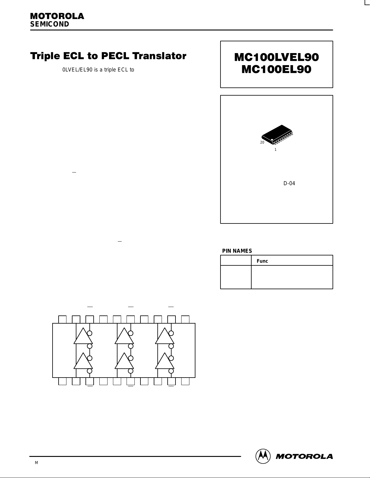
D2D1
Logic Diagram and Pinout: 20-Lead SOIC (Top View)
D1
1718 16 15 14 13 12
43
5 6 7 8 9
Q0
11
10
Q1 Q1 Q2 Q2 V
CC
D0
1920
21
VCCQ0
D0 D2V
CC
V
EE
GND
V
BB
GND
V
BB
ECL
PECL
ECL
PECL
ECL
PECL
DW SUFFIX
PLASTIC SOIC PACKAGE
CASE 751D-04
1
20
PIN NAMES
Function
ECL Inputs
PECL Outputs
ECL Reference Voltage Output
Pins
Dn
Qn
V
BB
MC100LVEL90 MC100EL90
MOTOROLA ECLinPS and ECLinPS Lite
DL140 — Rev 3
4–2
ECL INPUT DC CHARACTERISTICS
–40°C 0°C 25°C 85°C
Symbol Characteristic Min Max Min Max Min Typ Max Min Max Unit Condition
V
EE
Power Supply EL90
Voltage LVEL90
–4.2
–3.0
–5.5
–3.8
–4.2
–3.0
–5.5
–3.8
–4.2
–3.0
–5.5
–3.8
–4.2
–3.0
–5.5
–3.8
V
I
IH
Input HIGH Current 150 150 150 150 µA
I
IL
Input LOW Current 0.5 0.5 0.5 0.5 µA
V
PP
Minimum Peak-to-Peak
Input
1
150 150 150 150 mV
V
IH
Input HIGH Voltage –1165 –880 –1165 –880 –1165 –880 –1165 –880 V
V
IL
Input LOW Voltage –1810 –1475 –1810 –1475 –1810 –1475 –1810 –1475 V
V
BB
Reference Output –1.38 –1.26 –1.38 –1.26 –1.38 –1.26 –1.38 –1.26 V
I
EE
Power Supply Current 8.0 8.0 6.0 8.0 8.0 mA
1. 150mV input guarantees full logic swing at the output.
LVPECL OUTPUT DC CHARACTERISTICS
–40°C 0°C 25°C 85°C
Symbol Characteristic Min Max Min Max Min Typ Max Min Max Unit Condition
V
CC
Power Supply Voltage 3.0 3.8 3.0 3.8 3.0 3.3 3.8 3.0 3.8 V
V
OH
Output HIGH Voltage12.215 2.42 2.275 2.42 2.275 2.35 2.42 2.275 2.42 V VCC = 3.3V
V
OL
Output LOW Voltage
1
1.47 1.745 1.49 1.68 1.49 1.60 1.68 1.49 1.68 V VCC = 3.3V
I
GND
Power Supply Current 24 24 20 24 26 mA
1. Levels will vary 1:1 with VCC.
PECL OUTPUT DC CHARACTERISTICS
–40°C 0°C 25°C 85°C
Symbol Characteristic Min Max Min Max Min Typ Max Min Max Unit Condition
V
CC
Power Supply Voltage 4.75 5.25 4.75 5.25 4.75 5.25 4.75 5.25 V
V
OH
Output HIGH Voltage13.915 4.12 3.975 4.12 3.975 4.05 4.12 3.975 4.12 V VCC = 5.0V
V
OL
Output LOW Voltage
1
3.17 3.445 3.19 3.38 3.19 3.30 3.38 3.19 3.38 V VCC = 5.0V
I
GND
Power Supply Current 24 24 20 24 26 mA
1. Levels will vary 1:1 with VCC.

MC100LVEL90 MC100EL90
4–3 MOTOROLAECLinPS and ECLinPS Lite
DL140 — Rev 3
MC100LVEL90
AC CHARACTERISTICS (VEE = –3.0V to –3.8V; VCC = 3.0V to 3.8V)
–40°C 0°C 25°C 85°C
Symbol Characteristic Min Typ Max Min Typ Max Min Typ Max Min Typ Max Unit
t
PLH
t
PHL
Propagation Delay Diff
D to Q S.E.
390
340
590
640
410
360
610
660
420
370
620
670
460
410
660
710
ps
t
SKEW
Skew Output–to–Output
1
Part–to–Part (Diff)
1
Duty Cycle (Diff)
2
2025100
200
2025100
200
2025100
200
2025100
200
ps
V
PP
Minimum Input Swing
3
150 150 150 150 mV
V
CMR
Common Mode Range4See
4
–0.4 See
4
–0.4 See
4
–0.4 See
4
–0.4 V
t
r
t
f
Output Rise/Fall Times Q
(20% – 80%)
230 500 230 500 230 500 230 500
ps
1. Skews are valid across specified voltage range, part–to–part skew is for a given temperature.
2. Duty cycle skew is the difference between a TPLH and TPHL propagation delay through a device.
3. Minimum input swing for which AC parameters guaranteed. The device has a DC gain of ≈40.
4. The CMR range is referenced to the most positive side of the differential input signal. Normal operation is obtained if the HIGH level falls within
the specified range and the peak-to-peak voltage lies between VPPmin and 1V. V
CMR
min depends on VEE, VPP and temperature. At
VPP < 500mV and –40°C, V
CMR
is VEE +1.3V; and for 0–85°C, V
CMR
is VEE +1.2V . At VPP ≥ 500mV and –40°C, V
CMR
is VEE +1.5V; and for
0–85°C, V
CMR
is VEE +1.4V.
MC100EL90
AC CHARACTERISTICS (VEE = –4.20V to –5.5V; VCC = 4.5V to 5.5V)
–40°C 0°C 25°C 85°C
Symbol Characteristic Min Typ Max Min Typ Max Min Typ Max Min Typ Max Unit
t
PLH
t
PHL
Propagation Delay Diff
D to Q S.E.
390
340
590
640
410
360
610
660
420
370
620
670
460
410
660
710
ps
t
SKEW
Skew Output–to–Output
1
Part–to–Part (Diff)
1
Duty Cycle (Diff)
2
2025100
200
2025100
200
2025100
200
2025100
200
ps
V
PP
Minimum Input Swing
3
150 150 150 150 mV
V
CMR
Common Mode Range4See
4
–0.4 See
4
–0.4 See
4
–0.4 See
4
–0.4 V
t
r
t
f
Output Rise/Fall Times Q
(20% – 80%)
230 500 230 500 230 500 230 500
ps
1. Skews are valid across specified voltage range, part–to–part skew is for a given temperature.
2. Duty cycle skew is the difference between a TPLH and TPHL propagation delay through a device.
3. Minimum input swing for which AC parameters guaranteed. The device has a DC gain of ≈40.
4. The CMR range is referenced to the most positive side of the differential input signal. Normal operation is obtained if the HIGH level falls within
the specified range and the peak-to-peak voltage lies between VPPmin and 1V. V
CMR
min depends on VEE, VPP and temperature. At
VPP < 500mV and –40°C, V
CMR
is VEE +1.3V; and for 0–85°C, V
CMR
is VEE +1.2V . At VPP ≥ 500mV and –40°C, V
CMR
is VEE +1.5V; and for
0–85°C, V
CMR
is VEE +1.4V.

MC100LVEL90 MC100EL90
MOTOROLA ECLinPS and ECLinPS Lite
DL140 — Rev 3
4–4
OUTLINE DIMENSIONS
DW SUFFIX
PLASTIC SOIC PACKAGE
CASE 751D–04
ISSUE E
MIN MINMAX MAX
MILLIMETERS INCHES
DIM
A
B
C
D
F
G
J
K
M
P
R
0.510
0.299
0.104
0.019
0.035
0.012
0.009
7
°
0.415
0.029
0.499
0.292
0.093
0.014
0.020
0.010
0.004
0
°
0.395
0.010
12.95
7.60
2.65
0.49
0.90
0.32
0.25
7
°
10.55
0.75
12.65
7.40
2.35
0.35
0.50
0.25
0.10
0
°
10.05
0.25
NOTES:
1. DIMENSIONING AND TOLERANCING PER
ANSI Y14.5M, 1982.
2. CONTROLLING DIMENSION: MILLIMETER.
3. DIMENSIONS A AND B DO NOT INCLUDE
MOLD PROTRUSION.
4. MAXIMUM MOLD PROTRUSION 0.150
(0.006) PER SIDE.
5. DIMENSION D DOES NOT INCLUDE
DAMBAR PROTRUSION. ALLOWABLE
DAMBAR PROTRUSION SHALL BE 0.13
(0.005) TOTAL IN EXCESS OF D DIMENSION
AT MAXIMUM MATERIAL CONDITION.
1.27 BSC 0.050 BSC
–A
–
–B
–
P 10 PL
1 10
1120
–T
–
D
20 PL
K
C
SEATING
PLANE
R X 45°
M
0.010 (0.25)
B
M M
0.010 (0.25) T A B
M
S S
G 18 PL
F
J
Motorola reserves the right to make changes without further notice to any products herein. Motorola makes no warranty , representation or guarantee regarding
the suitability of its products for any particular purpose, nor does Motorola assume any liability arising out of the application or use of any product or circuit, and
specifically disclaims any and all liability , including without limitation consequential or incidental damages. “Typical” parameters which may be provided in Motorola
data sheets and/or specifications can and do vary in different applications and actual performance may vary over time. All operating parameters, including “Typicals”
must be validated for each customer application by customer’s technical experts. Motorola does not convey any license under its patent rights nor the rights of
others. Motorola products are not designed, intended, or authorized for use as components in systems intended for surgical implant into the body, or other
applications intended to support or sustain life, or for any other application in which the failure of the Motorola product could create a situation where personal injury
or death may occur. Should Buyer purchase or use Motorola products for any such unintended or unauthorized application, Buyer shall indemnify and hold Motorola
and its officers, employees, subsidiaries, affiliates, and distributors harmless against all claims, costs, damages, and expenses, and reasonable attorney fees
arising out of, directly or indirectly, any claim of personal injury or death associated with such unintended or unauthorized use, even if such claim alleges that
Motorola was negligent regarding the design or manufacture of the part. Motorola and are registered trademarks of Motorola, Inc. Motorola, Inc. is an Equal
Opportunity/Affirmative Action Employer.
How to reach us:
USA/EUROPE/Locations Not Listed: Motorola Literature Distribution; JAPAN: Nippon Motorola Ltd.; Tatsumi–SPD–JLDC, 6F Seibu–Butsuryu–Center,
P.O. Box 20912; Phoenix, Arizona 85036. 1–800–441–2447 or 602–303–5454 3–14–2 Tatsumi Koto–Ku, Tokyo 135, Japan. 03–81–3521–8315
MFAX: RMFAX0@email.sps.mot.com – TOUCHTONE 602–244–6609 ASIA/PACIFIC: Motorola Semiconductors H.K. Ltd.; 8B Tai Ping Industrial Park,
INTERNET: http://Design–NET.com 51 Ting Kok Road, Tai Po, N.T., Hong Kong. 852–26629298
MC100LVEL90/D
*MC100LVEL90/D*
◊

WWW.ALLDATASHEET.COM
Copyright © Each Manufacturing Company.
All Datasheets cannot be modified without permission.
This datasheet has been download from :
www.AllDataSheet.com
100% Free DataSheet Search Site.
Free Download.
No Register.
Fast Search System.
www.AllDataSheet.com
 Loading...