

Motorola MBRB2515L Datasheet
SEMICONDUCTOR TECHNICAL DATA
Order this document
by MBRB2515L/D
!
D2PAK Surface Mount Power Package
The D2P AK Power Rectifier employs the Schottky Barrier principle in a large
metal–to–silicon power diode. State–of–the–art geometry features epitaxial
construction with oxide passivation and metal overlay contact. Ideally suited for
use in low voltage, high frequency switching power supplies, free wheeling
diodes, and polarity protection diodes. These state–of–the–art devices have the
following features:
• Guardring for Stress Protection
• Low Forward Voltage
• 100°C Operating Junction Temperature
• Epoxy Meets UL94, VO at 1/8″
• Guaranteed Reverse Avalanche
• Short Heat Sink Tab Manufactured — Not Sheared!
• Similar in Size to the Industry Standard TO–220 Package
Mechanical Characteristics
• Case: Epoxy, Molded
• Weight: 1.7 grams (approximately)
• Finish: All External Surfaces Corrosion Resistant and Terminal
Leads are Readily Solderable
• Lead and Mounting Surface Temperature for Soldering
Purposes: 260°C Max. for 10 Seconds
• Shipped 50 units per plastic tube
• Available in 24 mm Tape and Reel, 800 units per 13″ reel by
adding a “T4” suffix to the part number
• Marking: B2515L
1
3
Motorola Preferred Device
SCHOTTKY BARRIER
RECTIFIER
25 AMPERES
15 VOLTS
4
4
1
3
CASE 418B–02
D2PAK
MAXIMUM RATINGS
Rating Symbol Value Unit
Peak Repetitive Reverse Voltage
Working Peak Reverse Voltage
DC Blocking Voltage
Average Rectified Forward Current (Rated VR) TC = 90°C I
Peak Repetitive Forward Current
(Rated VR, Square Wave, 20 kHz) TC = 100°C
Nonrepetitive Peak Surge Current
(Surge applied at rated load conditions halfwave, single phase, 60 Hz)
Storage Temperature T
Operating Junction Temperature T
Voltage Rate of Change (Rated VR) dv/dt 10000 V/µs
V
RRM
V
RWM
V
F(AV)
I
FRM
I
FSM
stg
15 Volts
R
25 Amps
30 Amps
150 Amps
–65 to +150 °C
J
100 °C
THERMAL CHARACTERISTICS
Thermal Resistance — Junction to Case
— Junction to Ambient (1)
(1) When mounted using minimum recommended pad size on FR–4 board.
Designer’s Data for “Worst Case” Conditions — The Designer’s Data Sheet permits the design of most circuits entirely from the information presented. SOA Limit
curves — representing boundaries on device characteristics — are given to facilitate “worst case” design.
Designer’s and SWITCHMODE are trademarks of Motorola, Inc.
Thermal Clad is a trademark of the Bergquist Company
Preferred devices are Motorola recommended choices for future use and best overall value.
R
R
θJC
θJA
1.0
50
°C/W
Rev 1
Rectifier Device Data
Motorola, Inc. 1996
1
MBRB2515L
ELECTRICAL CHARACTERISTICS
Rating Symbol Value Unit
Maximum Instantaneous Forward Voltage (2)
(IF = 19 Amps, TJ = 70°C)
(IF = 25 Amps, TJ = 70°C)
(IF = 25 Amps, TJ = 25°C)
Maximum Instantaneous Reverse Current (2)
(Rated dc Voltage, TJ = 70°C)
(Rated dc Voltage, TJ = 25°C)
(2) Pulse Test: Pulse Width = 300 µs, Duty Cycle ≤ 2.0%
V
F
I
R
0.28
0.42
0.45
200
15
Volts
mA
50
30
20
10
7.0
5.0
3.0
2.0
1.0
0.7
0.5
0.3
0.2
0.1
, INSTANTANEOUS FORWARD CURRENT (AMPS)
F
i
40
35
30
25
20
15
70°C
TJ = 25°C
0.1 0.2 0.4 4.0 8.0 12
vF, INSTANTANEOUS VOLTAGE (VOLTS)
0.30
0.5 20
1000
400
200
100
4.0
2.0
1.0
0.4
0.2
0.1
, REVERSE LEAKAGE CURRENT (mA)
0.04
R
I
0.02
0.01
40
20
10
2.0 6.0 10
0
TJ = 100°C
70°C
25°C
14
VR, REVERSE VOLTAGE (VOLTS)
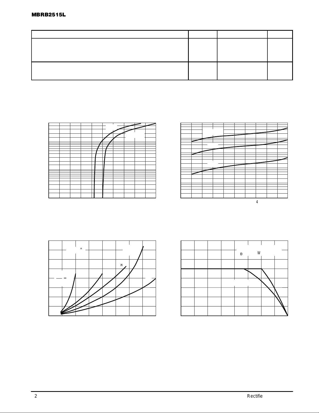
Figure 1. T ypical Forward Voltage Figure 2. T ypical Reverse Leakage Current
40
I
I
PK
AV
TJ = 70°C
+
10
5.0
SQUARE
WAVE
p
dc
35
30
25
20
15
RATED VOLTAGE APPLIED
R
= 1°C/W
q
JC
SQUARE WAVE
16
18
dc
, AVERAGE FORWARD POWER DISSIPATION (WATTS)
F(AV)
P
2
10
5.0
0
0
10 20 30 40 75 80 100
5.0 15 25 35
I
, AVERAGE FORW ARD CURRENT (AMPS)
F(AV )
10
, AVERAGE FORW ARD CURRENT (AMPS)
5.0
F(AV)
0
I
6560
70
TC, CASE TEMPERATURE (
Figure 3. T ypical Forward Power Dissipation Figure 4. Current Derating, Case
85 90 95
°
C)
Rectifier Device Data
 Loading...