


SEMICONDUCTOR TECHNICAL DATA
Order this document
by DTA143EE/D
PNP Silicon Surface Mount Transistor with
Monolithic Bias Resistor Network
The BRT (Bias Resistor Transistor) contains a single transistor with a monolithic
bias network consisting of two resistors; a series base resistor and a base–emitter
resistor. These digital transistors are designed to replace a single device and its
external resistor bias network. The BRT eliminates these individual components by
integrating them into a single device. The DTA143EE is housed in the
SOT–416/SC–90 package which is ideal for low–power surface mount applications
where board space is at a premium.
• Simplifies Circuit Design
• Reduces Board Space
• Reduces Component Count
• Available in 8 mm, 7 inch/3000 Unit Tape and Reel.
MAXIMUM RATINGS
Output Voltage V
Input Voltage V
Output Current I
DEVICE MARKING
DTA143EE = 43
THERMAL CHARACTERISTICS
Power Dissipation @ TA = 25°C
Operating and Storage Temperature Range TJ, T
Junction Temperature T
(TA = 25°C unless otherwise noted)
Rating Symbol Value Unit
(1)
O
I
O
P
D
stg
J
3
2
1
CASE 463–01, STYLE 1
SOT–416/SC–90
R
IN (1)
R1 = 4.7 k
R2 = 4.7 k
–55 to +150 °C
1
R
2
Ω
Ω
–50 Vdc
–30 Vdc
–100 mAdc
*125 mW
150 °C
OUT (3)
GND (2)
ELECTRICAL CHARACTERISTICS (T
Characteristic
Input Off Voltage (VO = –5.0 Vdc, IO = –100 µAdc) V
Input On Voltage (VO = –0.3 Vdc, IO = –20 mAdc) V
Output On Voltage (IO = –10 mAdc, II = –0.5 mAdc) V
Input Current (VI = –5.0 Vdc) I
Output Cutoff Current (VO = –50 Vdc) I
DC Current Gain (VO = –5.0 Vdc, IO = –10 mAdc) G
Input Resistance R
Resistance Ratio R1/R
1. Device mounted on a FR–4 glass epoxy printed circuit board using the minimum recommended footprint.
* Typical electrical characteristic curves are not available at this time.
This document contains information on a product under development. Motorola reserves the right to change or discontinue this product without notice.
Thermal Clad is a trademark of the Bergquist Company
Motorola Small–Signal Transistors, FETs and Diodes Device Data
Motorola, Inc. 1996
= 25°C)
A
Symbol Min Typ Max Unit
I(off)
I(on)
O(on)
I
O(off)
I
1
2
— — –0.5 Vdc
–3.0 — — Vdc
— — –0.3 Vdc
— — –1.8 mAdc
— — –500 nAdc
20 — — —
3.3 4.7 6.1 kOhms
0.8 1.0 1.2
1
DT A143EE
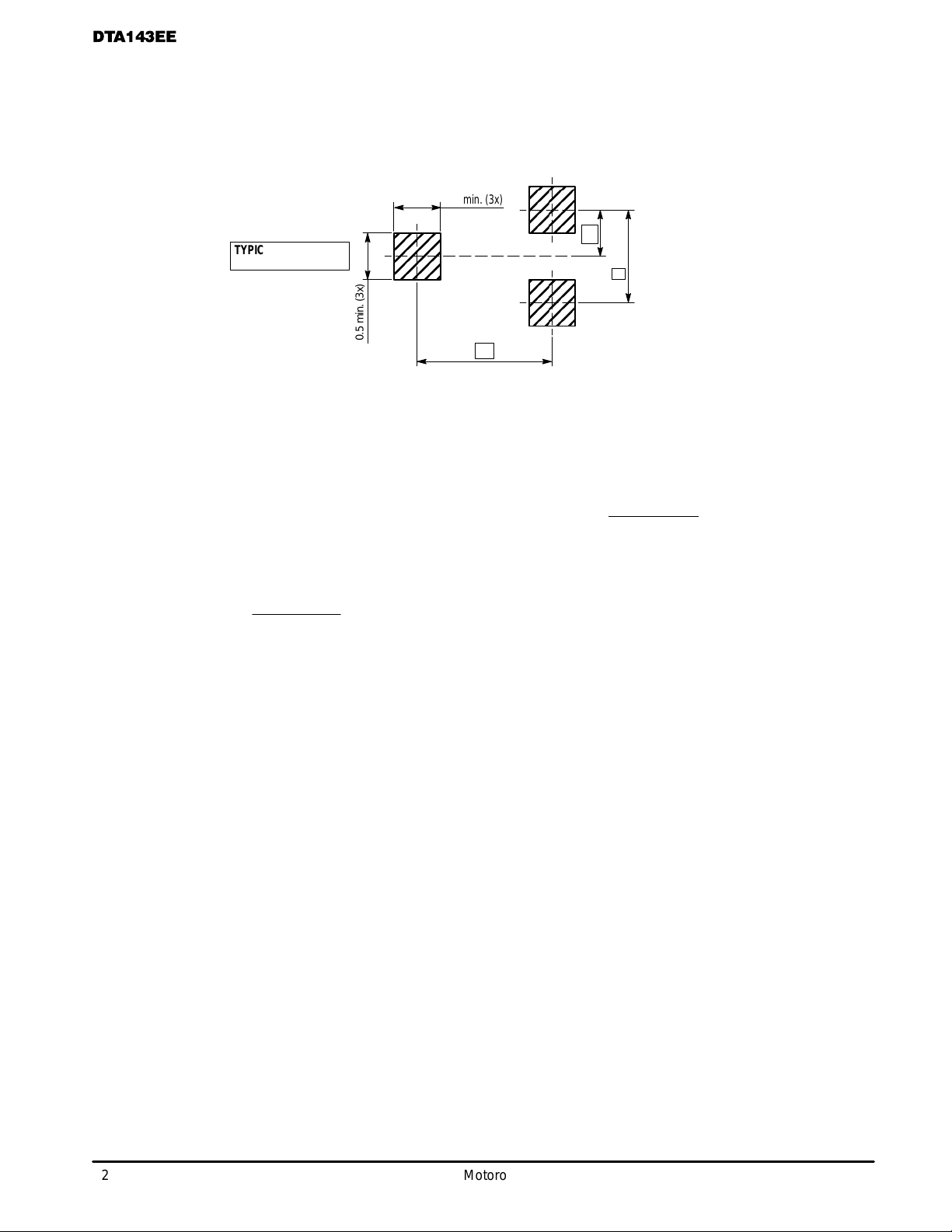
MINIMUM RECOMMENDED FOOTPRINTS FOR SURFACE MOUNTED APPLICATIONS
Surface mount board layout is a critical portion of the total
design. The footprint for the semiconductor packages must
be the correct size to insure proper solder connection
0.5 min. (3x)
TYPICAL
SOLDERING PATTERN
Unit: mm
0.5 min. (3x)
SOT–416/SC–90 POWER DISSIPATION
The power dissipation of the SOT–416/SC–90 is a function
of the pad size. This can vary from the minimum pad size for
soldering to the pad size given for maximum power
dissipation. Power dissipation for a surface mount device is
determined by T
ture of the die, R
junction to ambient; and the operating temperature, TA.
Using the values provided on the data sheet, PD can be
calculated as follows:
The values for the equation are found in the maximum
ratings table on the data sheet. Substituting these values into
, the maximum rated junction tempera-
J(max)
, the thermal resistance from the device
θJA
T
PD =
J(max)
R
θJA
– T
A
interface between the board and the package. With the
correct pad geometry, the packages will self align when
subjected to a solder reflow process.
0.5
1
1.4
the equation for an ambient temperature TA of 25°C, one can
calculate the power dissipation of the device which in this
case is 125 milliwatts.
150°C – 25°C
PD =
The 1000°C/W assumes the use of the recommended
footprint on a glass epoxy printed circuit board to achieve a
power dissipation of 125 milliwatts. Another alternative would
be to use a ceramic substrate or an aluminum core board
such as Thermal Clad. Using a board material such as
Thermal Clad, a higher power dissipation can be achieved
using the same footprint.
1000°C/W
= 125 milliwatts
SOLDERING PRECAUTIONS
The melting temperature of solder is higher than the rated
temperature of the device. When the entire device is heated
to a high temperature, failure to complete soldering within a
short time could result in device failure. Therefore, the
following items should always be observed in order to
minimize the thermal stress to which the devices are
subjected.
• Always preheat the device.
• The delta temperature between the preheat and
soldering should be 100°C or less.*
• When preheating and soldering, the temperature of the
leads and the case must not exceed the maximum
temperature ratings as shown on the data sheet. When
using infrared heating with the reflow soldering method,
the difference should be a maximum of 10°C.
• The soldering temperature and time should not exceed
260°C for more than 10 seconds.
• When shifting from preheating to soldering, the
maximum temperature gradient should be 5°C or less.
• After soldering has been completed, the device should
be allowed to cool naturally for at least three minutes.
Gradual cooling should be used as the use of forced
cooling will increase the temperature gradient and result
in latent failure due to mechanical stress.
• Mechanical stress or shock should not be applied during
cooling.
* Soldering a device without preheating can cause excessive
thermal shock and stress which can result in damage to the
device.
2
Motorola Small–Signal Transistors, FETs and Diodes Device Data
 Loading...