

Î
Î
Î
Î
Î
Î
Î
Î
Î
Î
Î
Î
Î
Î
Î
Î
Î
Î
Î
Î
查询BUD42D/D供应商
SEMICONDUCTOR TECHNICAL DATA
Order this document
by BUD42D/D
! ! "
"##$ " $"$
$#$%"$ $& "
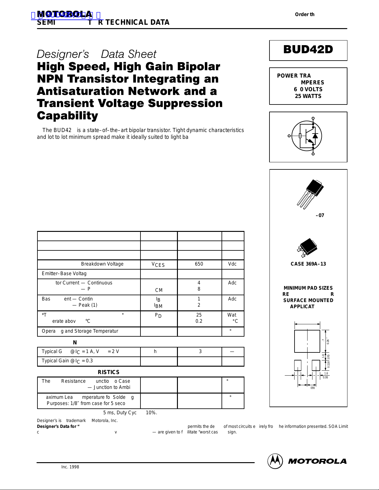
POWER TRANSISTORS
4 AMPERES
650 VOL TS
25 WATTS
"#$ $ %!!"##
!$'
The BUD42D is a state–of–the–art bipolar transistor. Tight dynamic characteristics
and lot to lot minimum spread make it ideally suited to light ballast applications.
Main features:
• Free Wheeling Diode built in
• Flat DC Current Gain
• Fast Switching Times and T ight Distribution
• “6 Sigma” Process Providing Tight and Reproducible Parameter Spreads
Two versions:
• BUD42D–1: Case 369–07 for Insertion Mode
• BUD42D: Case 369A–13 for Surface Mount Mode
MAXIMUM RATINGS
Parameters
Collector–Emitter Sustaining V oltage
Collector–Base Breakdown Voltage
Collector–Emitter Breakdown Voltage
Emitter–Base Voltage
Collector Current — Continuous
ОООООООООО
Base Current — Continuous
ОООООООООО
Base Current — Peak (1)
— Peak (1)
*Total Device Dissipation @ TC = 25_C
ОООООООООО
*Derate above 25°C
Operating and Storage Temperature
Symbol
V
CEO
V
CBO
V
CES
V
EBO
I
C
I
CM
ÎÎÎ
I
B
ÎÎÎ
I
BM
P
D
ÎÎÎ
TJ, T
stg
Value
350
650
650
9
4
8
ÎÎÎÎ
1
ÎÎÎÎ
2
25
ÎÎÎÎ
0.2
–65 to +150
Unit
Vdc
Vdc
Vdc
Vdc
Adc
Î
Adc
Î
Watt
Î
W/_C
_
C
TYPICAL GAIN
Typical Gain @IC = 1 A, VCE = 2 V
Typical Gain @IC = 0.3 A, VCE = 1 V
h
FE
h
FE
13
16
—
—
THERMAL CHARACTERISTICS
Thermal Resistance — Junction to Case
ОООООООООО
— Junction to Ambient
Maximum Lead Temperature for Soldering
Purposes: 1/8″ from case for 5 seconds
ОООООООООО
(1) Pulse Test: Pulse Width = 5 ms, Duty Cycle ≤ 10%.
Designer’s is a trademark of Motorola, Inc.
Designer’s Data for “Worst Case” Conditions — The Designer’s Data Sheet permits the design of most circuits entirely from the information presented. SOA Limit
curves — representing boundaries on device characteristics — are given to facilitate “worst case” design.
R
θJC
R
ÎÎÎ
θJA
T
L
ÎÎÎ
5
71.4
ÎÎÎÎ
260
ÎÎÎÎ
_
C/W
Î
Î
_
C
CASE 369–07
CASE 369A–13
MINIMUM PAD SIZES
RECOMMENDED FOR
SURFACE MOUNTED
APPLICATIONS
6.7
0.265
″
6.7
0.265
1.8
30
2.3
0.090
1.6
0.063
1.6
0.063
2.3
0.090
″
.070
0.118
Motorola, Inc. 1998
Motorola Bipolar Power Transistor Device Data
1
BUD42D
Î
Î
Î
Î
Î
Î
Î
Î
Î
Î
Î
Î
Î
Î
Î
Î
Î
Î
Î
Î
Î
Î
Î
Î
Î
Î
Î
Î
Î
Î
Î
Î
Î
Î
Î
Î
Î
Î
Î
Î
Î
Î
Î
ÎÎÎ
ÎÎÎ
Î
D
Î
I
A
ÎÎÎ
Î
Î
Î
ÎÎÎ
Î
Î
µ
Î
ÎÎÎ
Î
Î
Î
ÎÎÎ
Î
90% of final I
B1
I
200 mA
ÎÎÎ
ÎÎÎ
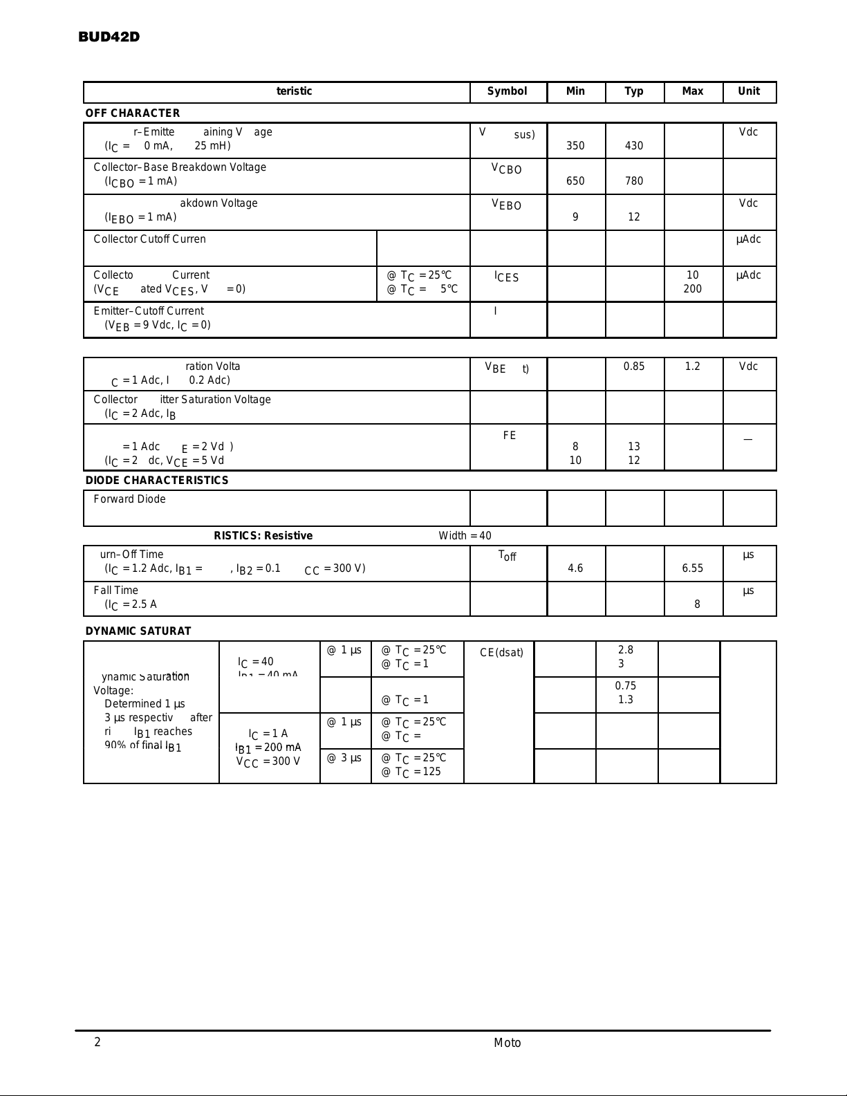
ELECTRICAL CHARACTERISTICS
Characteristic
(T
= 25°C unless otherwise noted)
C
Symbol
OFF CHARACTERISTICS
Collector–Emitter Sustaining Voltage
ОООООООООООООООООО
(IC = 100 mA, L = 25 mH)
Collector–Base Breakdown Voltage
(I
= 1 mA)
CBO
ОООООООООООООООООО
Emitter–Base Breakdown Voltage
(I
= 1 mA)
EBO
Collector Cutoff Current
ООООООООООООО
(VCE = Rated V
CEO
, IB = 0)
Collector Cutoff Current
(VCE = Rated V
ООООООООООООО
CES
, VEB = 0)
@ TC = 25°C
ÎÎÎÎ
@ TC = 125°C
@ TC = 25°C
@ TC = 125°C
ÎÎÎÎ
Emitter–Cutoff Current
V
CEO(sus)
ÎÎ
V
ÎÎ
V
I
ÎÎ
I
ÎÎ
I
(VEB = 9 Vdc, IC = 0)
ON CHARACTERISTICS
Base–Emitter Saturation Voltage
ОООООООООООООООООО
(IC = 1 Adc, IB = 0.2 Adc)
Collector–Emitter Saturation Voltage
(IC = 2 Adc, IB = 0.5 Adc)
ОООООООООООООООООО
DC Current Gain
ОООООООООООООООООО
(IC = 1 Adc, VCE = 2 Vdc)
(IC = 2 Adc, VCE = 5 Vdc)
ОООООООООООООООООО
V
BE(sat)
ÎÎ
V
CE(sat)
ÎÎ
ÎÎ
ÎÎ
DIODE CHARACTERISTICS
Forward Diode Voltage
ОООООООООООООООООО
(IEC = 1.0 Adc)
V
ÎÎ
SWITCHING CHARACTERISTICS: Resistive Load (D.C.≤ 10%, Pulse Width = 40 µs)
Turn–Off Time
(IC = 1.2 Adc, IB1 = 0.4 A, IB2 = 0.1 A, VCC = 300 V)
ОООООООООООООООООО
ÎÎ
Fall Time
(IC = 2.5 Adc, IB1 = IB2 = 0.5 A, VCC = 150 V, VBE = –2 V)
ОООООООООООООООООО
ÎÎ
DYNAMIC SATURATION VOLTAGE
V
CE(dsat)
ÎÎÎÎÎÎ
ÎÎÎÎÎÎ
ynamic Saturation
Voltage:
ОООООО
Determined 1 µs and
3 µs respectively after
rising IB1 reaches
ОООООО
IC = 400 mA
= 40 m
B1
VCC = 300 V
ÎÎÎÎ
IC = 1 A
ÎÎÎÎ
=
B1
VCC = 300 V
@ 1 µs
@ 3 µs
ÎÎ
@ 1 µs
ÎÎ
@ 3 µs
@ TC = 25°C
@ TC = 125°C
@ TC = 25°C
ÎÎÎ
@ TC = 125°C
@ TC = 25°C
@ TC = 125°C
ÎÎÎ
@ TC = 25°C
@ TC = 125°C
CBO
EBO
CEO
CES
EBO
h
FE
EC
T
off
T
f
Min
ÎÎ
350
650
ÎÎ
9
Typ
ÎÎ
430
780
ÎÎ
12
Max
ÎÎ
ÎÎ
100
ÎÎÎÎÎÎÎÎ
200
10
ÎÎÎÎÎÎÎÎ
200
100
ÎÎÎÎÎ
0.85
1.2
ÎÎ
0.2
ÎÎ
ÎÎ
8
10
ÎÎ
ÎÎÎÎÎ
4.6
ÎÎ
ÎÎÎÎÎÎÎÎ
ÎÎ
ÎÎ
13
12
ÎÎ
0.9
ÎÎÎÎÎ
ÎÎ1ÎÎ
ÎÎ
ÎÎ
ÎÎ
1.5
6.55
0.8
2.8
3.2
0.75
ÎÎÎ
ÎÎÎÎÎ
1.3
2.1
4.7
ÎÎÎ
ÎÎÎÎÎ
0.35
0.6
Unit
Vdc
ÎÎ
Vdc
ÎÎ
Vdc
µAdc
ÎÎ
µAdc
ÎÎ
µAdc
Vdc
ÎÎ
Vdc
—
ÎÎ
ÎÎ
V
ÎÎ
µs
ÎÎ
µs
ÎÎ
V
2
Motorola Bipolar Power Transistor Device Data
TYPICAL STATIC CHARACTERISTICS
BUD42D
100
10
, DC CURRENT GAIN
FE
h
TJ = 125°C
TJ = 25°C
TJ = –20°C
1
IC, COLLECTOR CURRENT (AMPS)
Figure 1. DC Current Gain @ VCE = 1 V
3
2 A
2
TJ = 25°C
100
TJ = 125°C
TJ = 25°C
10
TJ = –20°C
, DC CURRENT GAIN
FE
h
1010.10.010.001
1
IC, COLLECTOR CURRENT (AMPS)
1010.10.010.001
Figure 2. DC Current Gain @ VCE = 5 V
10
IC/IB = 5
1
, VOLTAGE (VOLTS)
CE
V
, VOLTAGE (VOLTS)
CE
V
100
10
0.1
1.5 A
TJ = 125
°
TJ = 125
C
TJ = –20°C
TJ = –20°C
°
C
TJ = 25°C
1010.10.010.001
TJ = 25°C
1
IC = 0.2 A
0
1 A
0.4 A
1
IB, BASE CURRENT (AMPS)
100.10.010.001
Figure 3. Collector Saturation Region
IC/IB = 8
TJ = 125°C
1
TJ = –20°C
TJ = 25°C
, VOLTAGE (VOLTS)
0.1
CE
V
0.01
IC, COLLECTOR CURRENT (AMPS)
Figure 4. Collector–Emitter Saturation V oltage
10
IC/IB = 10
1
, VOLTAGE (VOLTS)
0.1
CE
V
0.01
1
IC, COLLECTOR CURRENT (AMPS)
Figure 5. Collector–Emitter Saturation V oltage
Motorola Bipolar Power Transistor Device Data
100.10.010.001
0.01
IC, COLLECTOR CURRENT (AMPS)
1
100.10.010.001
Figure 6. Collector–Emitter Saturation V oltage
3

BUD42D
TYPICAL STATIC CHARACTERISTICS
, VOLTAGE (VOLTS)
BE
V
10
IC/IB = 5
1
TJ = –20°C
TJ = 125°C
0.1
TJ = 25°C
IC, COLLECTOR CURRENT (AMPS)
Figure 7. Base–Emitter Saturation Region
10
IC/IB = 10
10
IC/IB = 8
1
TJ = –20°C
, VOLTAGE (VOLTS)
BE
V
TJ = 125°C TJ = 25°C
1
100.10.010.001
0.1
IC, COLLECTOR CURRENT (AMPS)
1
100.10.010.001
Figure 8. Base–Emitter Saturation Region
10
, VOLTAGE (VOLTS)
BE
V
1
TJ = –20°C
TJ = 125°C
0.1
TJ = 25°C
IC, COLLECTOR CURRENT (AMPS)
Figure 9. Base–Emitter Saturation Region
V
1
FORWARD DIODE VOLTAGE (VOLTS)
1
100.10.010.001
0.1
= –20°C
EC(V)
V
= 125°C
EC(V)
REVERSE EMITTER–COLLECTOR CURRENT
V
EC(V)
= 25°C
1
100.10.01
Figure 10. Forward Diode Voltage
4
Motorola Bipolar Power Transistor Device Data

TYPICAL SWITCHING CHARACTERISTICS
BUD42D
1000
C, CAPACITANCE (pF)
t, TIME (ns)
100
10
800
700
600
500
400
300
200
100
900
C
ib
1
VR, REVERSE VOLTAGE (VOLTS)
Figure 11. Capacitance
hFE = 10
hFE = 5
TJ = 125°C
TJ = 25
°
C
0
0.5 1.5
IC, COLLECTOR CURRENT (AMPS)
TJ = 25°C
f
= 1 MHz
(test)
I
Bon
VCC = 300 V
PW = 40
= I
C
Boff
ob
µ
800
I
= 10 mA
700
(VOLTS)
600
VCER
B
500
400
TC = 25°C
100101
s
210
300
9
6
t, TIME (ns)
3
TJ = 125°C
TJ = 25
0
I
= 100 mA
CER
lC = 25 mH
RBE (W)
Figure 12. B
°
C
IC, COLLECTOR CURRENT (AMPS)
VCER
hFE = 10
1
CER
1000
= f(RBE)
I
Bon
VCC = 300 V
PW = 40
1.5
= I
Boff
hFE = 5
1000010010
µ
s
20.50
Figure 13. Resistive Switching, t
4
I
= I
Bon
3
µ
2
t, TIME ( s)
1
0
0
Boff
VCE = 15 V
VZ = 300 V
LC = 200
µ
H
0.5 1 1.5 2
IC, COLLECTOR CURRENT (AMPS)
TJ = 125°C
TJ = 25
Figure 15. Inductive Storage Time,
tsi @ hFE = 5
Motorola Bipolar Power Transistor Device Data
on
4
3
°
C
µ
t, TIME ( s)
2
1
Figure 14. Resistive Switching, t
I
Bon
VCE = 15 V
TJ = 125°C
TJ = 25
°
C
IC, COLLECTOR CURRENT (AMPS)
VZ = 300 V
LC = 200
1.5
off
= I
Boff
µ
H
210.5
Figure 16. Inductive Storage Time,
tsi @ hFE = 10
5

BUD42D
TYPICAL SWITCHING CHARACTERISTICS
400
300
t, TIME (ns)
200
100
I
= I
Bon
Boff
VCC = 15 V
VZ = 300 V
LC = 200
µ
H
0.5 1.5
IC, COLLECTOR CURRENT (AMPS)
Figure 17. Inductive Fall and Cross Over Time,
tfi and tc @ hFE = 5
500
I
= I
Bon
Boff
VCC = 15 V
400
t, TIME (ns)
300
VZ = 300 V
LC = 200
µ
H
TJ = 125°C
TJ = 25
t
c
t
fi
TJ = 125°C
TJ = 25°C
250
°
C
1.5
TJ = 125°C
TJ = 25°C
210.5
200
t, TIME (ns)
210
150
100
I
= I
Bon
Boff
VCE = 15 V
VZ = 300 V
LC = 200
µ
H
IC, COLLECTOR CURRENT (AMPS)
Figure 18. Inductive Fall Time,
tfi @ hFE = 10
5
I
= I
Bon
4
m
3
t, TIME ( s)
2
Boff
VCC = 15 V
VZ = 300 V
LC = 200
µ
I
= 1 A
C
IC = 0.3 A
H
TJ = 125°C
TJ = 25
°
C
, FALL TIME (ns)
fi
t
200
IC, COLLECTOR CURRENT (AMPS)
Figure 19. Inductive Cross Over Time,
tc @ hFE = 10
300
I
= I
Bon
Boff
VCC = 15 V
VZ = 300 V
LC = 200
µ
H
200
100
hFE, FORCED GAIN
Figure 21. Inductive Fall Time, t
1.5
210.5
1
Figure 20. Inductive Storage Time, t
300
IC = 0.3 A
IC = 1 A
TJ = 125°C
TJ = 25
°
C
759
1063
f
200
CROSS–OVER TIME (ns)
100
Figure 22. Inductive Cross Over Time, t
5
hFE, FORCED GAIN
IC = 1 A
hFE, FORCED GAIN
76810911
1243
si
IC = 0.3 A
I
= I
Bon
Boff
VCC = 15 V
TJ = 125°C
TJ = 25
°
C
648
VZ = 300 V
LC = 200
8
µ
H
1042
c
6
Motorola Bipolar Power Transistor Device Data

TYPICAL SWITCHING CHARACTERISTICS
BUD42D
3
I
= I
Bon
Boff
VCC = 15 V
VZ = 300 V
2.5
LC = 200
m
2
t, TIME ( s)
1.5
1
Figure 23. Inductive Storage Time, t
V
CE
0 V
90% I
I
B
IB 1 & 2 = 200 mA
µ
H
50 mA
0.5 1.5
IC, COLLECTOR CURRENT (AMPS)
Dyn 1 ms
Dyn 3 ms
B
1 ms
3 ms
100 mA
500 mA
si
440
420
400
380
360
340
, FORWARD RECOVERY TIME (ns)
fr
320
t
210
300
IF, FORWARD CURRENT (AMPS)
Figure 24. Forward Recovery Time, t
10
I
C
8
6
V
clamp
4
I
B
2
90% I
10% V
B1
di/dt = 10 A/ms, TC = 25°C
1
90% I
t
si
clamp
C
1.5
20.50
fr
t
fi
10% I
C
t
c
TIME
Figure 25. Dynamic Saturation V oltage
Measurements
0
2
40
TIME
68
Figure 26. Inductive Switching Measurements
Motorola Bipolar Power Transistor Device Data
7

BUD42D
+15 V
1
µ
TYPICAL SWITCHING CHARACTERISTICS
T able 1. Inductive Load Switching Drive Circuit
100
µ
F
150
3 W
100
Ω
Ω
3 W
MTP8P10
F
VCE PEAK
IC PEAK
+10 V
COMMON
–V
off
MPF930
Ω
50
MPF930
µ
500
MTP8P10
MUR105
MJE210
F
10% I
MTP12N10
F
Ω
150
F
3 W
F
V
F
I
0.1 V
R
B1
I
out
A
R
B2
1
µ
F
V
FRM
t
fr
VFR (1.1 VF) UNLESS
OTHERWISE SPECIFIED
V
CE
I
B1
I
B
V
(BR)CEO(sus)
L = 10 mH
RB2 =
∞
VCC = 20 Volts
I
= 100 mA
C(pk)
I
B2
Inductive Switching
L = 200
µ
H
RB2 = 0
VCC = 15 Volts
RB1 selected for
desired I
B1
RBSOA
L = 500
µ
H
RB2 = 0
VCC = 15 Volts
RB1 selected for
desired I
B1
10
1 ms
1
0.1
, COLLECTOR CURRENT (AMPS)
C
I
0.01
5 ms
dc
VCE, COLLECTOR–EMITTER VOL TAGE (VOLTS)
Figure 28. Forward Bias Safe Operating Area
8
Figure 27. tfr Measurement
MAXIMUM RATINGS
10 ms
1 ms
EXTENDED SOA
100010010
5
4
3
2
V
1
C
I , COLLECTOR CURRENT (AMPS)
0
VBE = 0 V V
VCE, COLLECTOR–EMITTER VOL TAGE (VOLTS)
BE(off)
= –1.5 V
BE(off)
Figure 29. Reverse Bias Safe Operating Area
Motorola Bipolar Power Transistor Device Data
TJ = 125°C
GAIN
LC = 500
= –5 V
600
≥
4
m
H
700500400300

BUD42D
1
0.8
0.6
0.4
POWER DERATING F ACT OR
0.2
0
60
TC, CASE TEMPERATURE (
Figure 30. Power Derating
There are two limitations on the power handling ability of a
transistor: average junction temperature and second breakdown. Safe operating area curves indicate IC–VCE limits of
the transistor that must be observed for reliable operation;
i.e., the transistor must not be subjected to greater dissipation than the curves indicate. The data of Figure 28 is based
on TC = 25°C; T
is variable depending on power level.
j(pk)
Second breakdown pulse limits are valid for duty cycles to
10% but must be derated when TC > 25°C. Second Breakdown limitations do not derate like thermal limitations. Allowable current at the voltages shown on Figure 28 may be
SECOND BREAKDOWN
DERATING
THERMAL DERATING
80 100 120 140
°
C)
found at any case temperature by using the appropriate
curve on Figure 30.
T
may be calculated from the data in Figure 31. At any
j(pk)
case temperatures, thermal limitations will reduce the power
that can be handled to values less than the limitations imposed by second breakdown. For inductive loads, high voltage and current must be sustained simultaneously during
turn–off with the base to emitter junction reverse biased. The
safe level is specified as reverse biased safe operating area
(Figure 29). This rating is verified under clamped conditions
so that the device is never subjected to an avalanche mode.
1604020
1
D = 0.5
0.2
0.1
0.05
0.1
0.02
0.01
r(t) TRANSIENT THERMAL
RESISTANCE (NORMALIZED)
SINGLE PULSE
0.01
P
(pk)
t
1
DUTY CYCLE, D = t1/t
1010.1
t, TIME (ms)
Figure 31. Thermal Response
R
(t) = r(t) R
θ
JC
R
θ
JC
D CURVES APPLY FOR POWER
PULSE TRAIN SHOWN
t
2
READ TIME AT t
T
2
J(pk)
θ
= 5°C/W MAX
– TC = P
JC
1
(pk)
R
(t)
θ
JC
10001000.01
Motorola Bipolar Power Transistor Device Data
9

BUD42D
P ACKAGE DIMENSIONS
V
–T–
SEATING
PLANE
V
S
S
F
F
B
R
4
123
G
B
R
4
123
G
A
K
3 PL
D
0.13 (0.005) T
A
K
L
D
2 PL
0.13 (0.005) T
C
E
J
H
M
CASE 369–07
ISSUE L
SEATING
–T–
PLANE
C
E
Z
U
J
H
M
CASE 369A–13
ISSUE Z
NOTES:
1. DIMENSIONING AND TOLERANCING PER ANSI
Y14.5M, 1982.
2. CONTROLLING DIMENSION: INCH.
DIM MIN MAX MIN MAX
A 0.235 0.250 5.97 6.35
B 0.250 0.265 6.35 6.73
C 0.086 0.094 2.19 2.38
D 0.027 0.035 0.69 0.88
E 0.033 0.040 0.84 1.01
F 0.037 0.047 0.94 1.19
0.090 BSC 2.29 BSC
G
H 0.034 0.040 0.87 1.01
J 0.018 0.023 0.46 0.58
K 0.350 0.380 8.89 9.65
R 0.175 0.215 4.45 5.46
S 0.050 0.090 1.27 2.28
V 0.030 0.050 0.77 1.27
STYLE 1:
PIN 1. BASE
2. COLLECTOR
3. EMITTER
4. COLLECTOR
NOTES:
1. DIMENSIONING AND TOLERANCING PER ANSI
Y14.5M, 1982.
2. CONTROLLING DIMENSION: INCH.
DIM MIN MAX MIN MAX
A 0.235 0.250 5.97 6.35
B 0.250 0.265 6.35 6.73
C 0.086 0.094 2.19 2.38
D 0.027 0.035 0.69 0.88
E 0.033 0.040 0.84 1.01
F 0.037 0.047 0.94 1.19
G 0.180 BSC 4.58 BSC
H 0.034 0.040 0.87 1.01
J 0.018 0.023 0.46 0.58
K 0.102 0.114 2.60 2.89
L 0.090 BSC 2.29 BSC
R 0.175 0.215 4.45 5.46
S 0.020 0.050 0.51 1.27
U 0.020 ––– 0.51 –––
V 0.030 0.050 0.77 1.27
Z 0.138 ––– 3.51 –––
STYLE 1:
PIN 1. BASE
2. COLLECTOR
3. EMITTER
4. COLLECTOR
MILLIMETERSINCHES
MILLIMETERSINCHES
Motorola reserves the right to make changes without further notice to any products herein. Motorola makes no warranty , representation or guarantee regarding
the suitability of its products for any particular purpose, nor does Motorola assume any liability arising out of the application or use of any product or circuit, and
specifically disclaims any and all liability, including without limitation consequential or incidental damages. “T ypical” parameters which may be provided in Motorola
data sheets and/or specifications can and do vary in different applications and actual performance may vary over time. All operating parameters, including “Typicals”
must be validated for each customer application by customer’s technical experts. Motorola does not convey any license under its patent rights nor the rights of
others. Motorola products are not designed, intended, or authorized for use as components in systems intended for surgical implant into the body, or other
applications intended to support or sustain life, or for any other application in which the failure of the Motorola product could create a situation where personal injury
or death may occur. Should Buyer purchase or use Motorola products for any such unintended or unauthorized application, Buyer shall indemnify and hold Motorola
and its officers, employees, subsidiaries, affiliates, and distributors harmless against all claims, costs, damages, and expenses, and reasonable attorney fees
arising out of, directly or indirectly, any claim of personal injury or death associated with such unintended or unauthorized use, even if such claim alleges that
Motorola was negligent regarding the design or manufacture of the part. Motorola and are registered trademarks of Motorola, Inc. Motorola, Inc. is an Equal
Opportunity/Affirmative Action Employer.
Mfax is a trademark of Motorola, Inc.
How to reach us:
USA/EUROPE/Locations Not Listed: Motorola Literature Distribution; JAPAN: Nippon Motorola Ltd.; SPD, Strategic Planning Office, 141,
P.O. Box 5405, Denver, Colorado 80217. 1–303–675–2140 or 1–800–441–2447 4–32–1 Nishi–Gotanda, Shinagawa–ku, Tokyo, Japan. 81–3–5487–8488
Customer Focus Center: 1–800–521–6274
Mfax: RMFAX0@email.sps.mot.com – TOUCHTONE 1–602–244–6609 ASIA/PACIFIC: Motorola Semiconductors H.K. Ltd.; 8B Tai Ping Industrial Park,
Moto rola Fax Back System – US & Canada ONLY 1–800–774–1848 51 Ting Kok Road, Tai Po, N.T., Hong Kong. 852–26629298
– http://sps.motorola.com/mfax/
HOME PAGE: http://motorola.com/sps/
10
◊
Motorola Bipolar Power Transistor Device Data
BUD42D/D
 Loading...