SEMICONDUCTOR
TECHNICAL DATA
QUAD EIA–422 LINE DRIVER
WITH THREE–STATE OUTPUTS
PIN CONNECTIONS
Order this document by AM26LS31/D
PC SUFFIX
PLASTIC PACKAGE
CASE 648
D SUFFIX
PLASTIC PACKAGE
CASE 751B
(SO–16)
Device
Operating
Temperature Range
Package
ORDERING INFORMATION
AM26LS31PC
MC26LS31D*
TA = 0 to +70°C
Plastic DIP
SO–16
11
10
Outputs C
9
6
5
Outputs D
13
14
Outputs A
3
2
8
7
4
1
12
15
Outputs B
Enable
V
CC
Input C
Input D
Input A
16
Enable
Input B
Gnd
1
MOTOROLA ANALOG IC DEVICE DATA
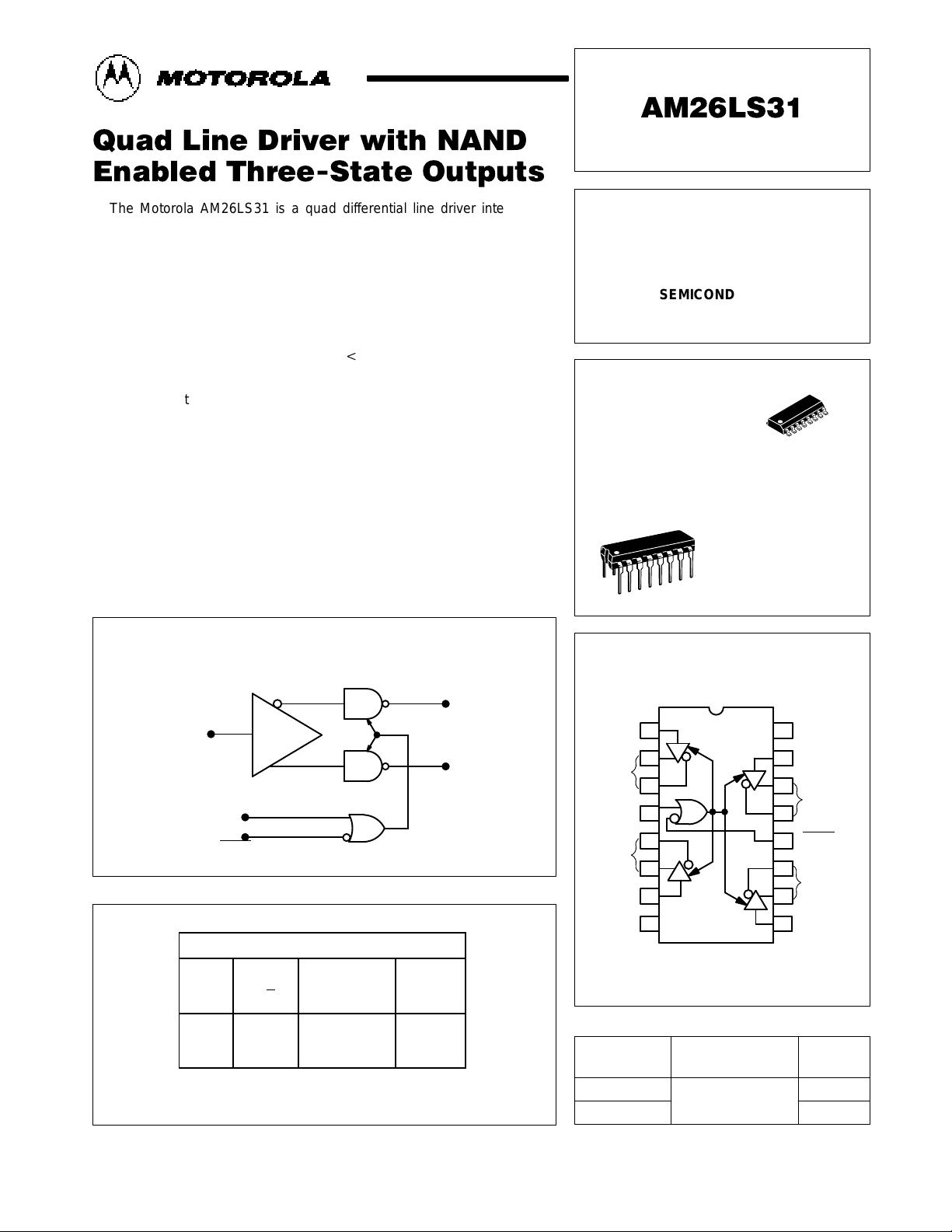
The Motorola AM26LS31 is a quad differential line driver intended for
digital data transmission over balanced lines. It meets all the requirements of
EIA–422 Standard and Federal Standard 1020.
The AM26LS31 provides an enable/disable function common to all four
drivers as opposed to the split enables on the MC3487 EIA–422 driver.
The high impedance output state is assured during power down.
• Full EIA–422 Standard Compliance
• Single +5.0 V Supply
• Meets Full V
O
= 6.0 V, VCC = 0 V, IO t 100 µA Requirement
• Output Short Circuit Protection
• Complementary Outputs for Balanced Line Operation
• High Output Drive Capability
• Advanced LS Processing
• PNP Inputs for MOS Compatibility
Representative Block Diagrams
Enable
Enable
Input
Non–Inverting
Outputs
Inverting
Output
Controls
TRUTH TABLE
Input
Control
lnputs
(E/E
)
Non–Inverting
Output
Inverting
Output
H
L
X
H/L
H/L
L/H
H
L
Z
L
H
Z
* Note that the surface mount MC26LS31D device uses the same die as in the plastic DIP
* AM26LS31DC device, but with an MC prefix to prevent confusion with the package suffix.
Motorola, Inc. 1995
X = Irrelevant
Z = Third–State (High Impedance)
L = Low Logic State
H = High Logic State

AM26LS31
2
MOTOROLA ANALOG IC DEVICE DATA
MAXIMUM RATINGS
Rating Symbol Value Unit
Power Supply Voltage V
CC
8.0 Vdc
Input Voltage V
I
5.5 Vdc
Operating Ambient Temperature Range T
A
0 to + 70 °C
Operating Junction Temperature Range T
J
150 °C
Storage Temperature Range T
stg
– 65 to + 150 °C
ELECTRICAL CHARACTERISTICS (Unless otherwise noted, specifications apply 4.75 V
p
VCC p 5.25 V and 0°C p TA p 70°C.
Typical values measured at VCC = 5.0 V, and TA = 25°C.)
Characteristic
Symbol Min Typ Max Unit
Input Voltage – Low Logic State V
IL
– – 0.8 Vdc
Input Voltage – High Logic State V
IH
2.0 – – Vdc
Input Current – Low Logic State
(VIL = 0.4 V)
I
IL
– – – 360 µA
Input Current – High Logic State
(VIH = 2.7 V)
(VIH = 7.0 V)
I
IH
–
–
–
–
+ 20
+ 100
µA
Input Clamp Voltage
(IIK = – 18 mA)
V
IK
– – – 1.5 V
Output Voltage – Low Logic State
(IOL = 20 mA)
V
OL
– – 0.5 V
Output Voltage – High Logic State
(IOH = –20 mA)
V
OH
2.5 – – V
Output Short Circuit Current
(VIH = 2.0 V) Note 1
I
OS
– 30 – – 150 mA
Output Leakage Current – Hi–Z State
(VOL = 0.5 V, V
IL(E)
= 0.8 V, V
IH(E
)
= 2.0 V)
(VOH = 2.5 V, V
IL(E)
= 0.8 V, V
IH(E
)
= 2.0 V)
I
O(Z)
–
–
–
–
– 20
+ 20
µA
Output Leakage Current – Power OFF
(VOH = 6.0 V, VCC = 0 V)
(VOL = – 0.25 V, VCC = 0 V)
I
O(off)
–
–
–
–
+ 100
– 100
µA
Output Offset Voltage Difference, Note 2 VOS – V
OS
– –
"
0.4 V
Output Differential Voltage, Note 2 V
OD
2.0 – – V
Output Differential Voltage Difference, Note 2 ∆VOD – – ± 0.4 V
Power Supply Current
(Output Disabled) Note 3
I
CCX
– 60 80 mA
NOTES: 1. Only one output may be shorted at a time.
2.See EIA Specification EIA–422 for exact test conditions.
3.Circuit in three–state condition.
SWITCHING CHARACTERISTICS (V
CC
= 5.0 V, TA = 25°C unless otherwise noted.)
Characteristic
Symbol Min Typ Max Unit
Propagation Delay Times
High to Low Output
Low to High Output
t
PHL
t
PLH
–
–
–
–
20
20
ns
Output Skew – – 6.0 ns
Propagation Delay – Control to Output
(CL = 10 pF, RL = 75 Ω to Gnd)
(CL = 10 pF, RL = 180 Ω to VCC)
(CL = 30 pF, RL = 75 Ω to Gnd)
(CL = 30 pF, RL = 180 Ω to VCC)
t
PHZ(E)
t
PLZ(E)
t
PZH(E)
t
PZL(E)
–
–
–
–
–
–
–
–
30
35
40
45
ns
 Loading...