Motorola 2SA1774 Datasheet

SEMICONDUCTOR TECHNICAL DATA
Order this document
by 2SA1774/D
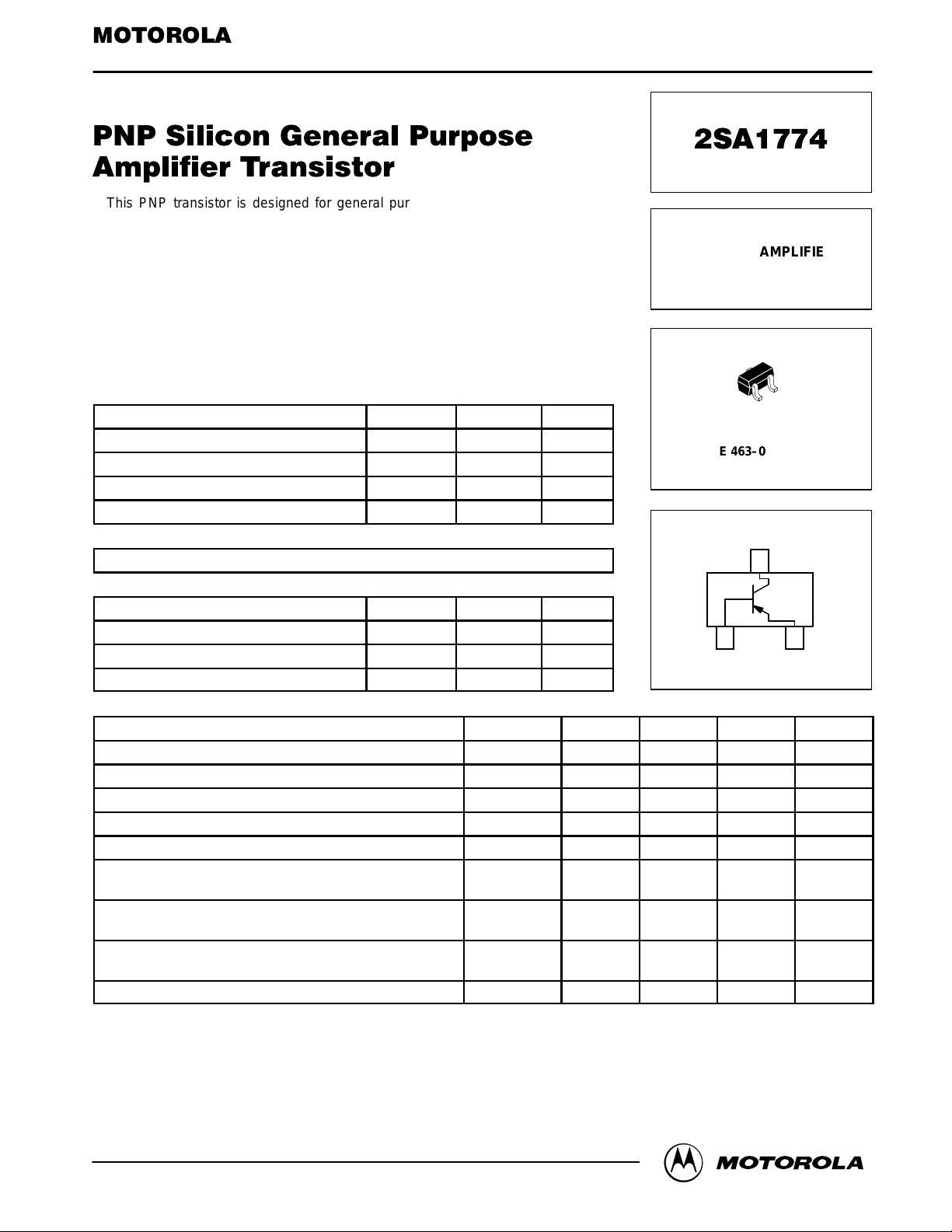
This PNP transistor is designed for general purpose amplifier applications. This
device is housed in the SOT–416/SC–90 package which is designed for low power
surface mount applications, where board space is at a premium.
• Reduces Board Space
• High hFE, 210–460 (typical)
• Low V
CE(sat)
• Available in 8 mm, 7–inch/3000 Unit Tape and Reel
MAXIMUM RATINGS
Collector–Base Voltage V
Collector–Emitter Voltage V
Emitter–Base Voltage V
Collector Current — Continuous I
DEVICE MARKING
2SA1774 = F9
THERMAL CHARACTERISTICS
Power Dissipation
Junction Temperature T
Storage Temperature Range T
ELECTRICAL CHARACTERISTICS (T
Collector–Base Breakdown Voltage (IC = –50 µAdc, IE = 0) V
Collector–Emitter Breakdown Voltage (IC = –1.0 mAdc, IB = 0) V
Emitter–Base Breakdown Voltage (IE = –50 µAdc, IE = 0) V
Collector–Base Cutoff Current (VCB = –30 Vdc, IE = 0) I
Emitter–Base Cutoff Current (VEB = –5.0 Vdc, IB = 0) I
Collector–Emitter Saturation Voltage
(IC = –50 mAdc, IB = –5.0 mAdc)
DC Current Gain
(VCE = –6.0 Vdc, IC = –1.0 mAdc)
Transition Frequency
(VCE = –12 Vdc, IC = –2.0 mAdc, f = 30 MHz)
Output Capacitance (VCB = –12 Vdc, IE = 0 Adc, f = 1 MHz) C
1. Device mounted on a FR–4 glass epoxy printed circuit board using the minimum recommended footprint.
2. Pulse Test: Pulse Width ≤ 300 µs, D.C. ≤ 2%.
, < 0.5 V
(TA = 25°C)
Rating Symbol Value Unit
(BR)CBO
(BR)CEO
(BR)EBO
C
Rating Symbol Max Unit
(1)
= 25°C)
A
Characteristic Symbol Min Typ Max Unit
(2)
(2)
P
D
J
stg
–60 Vdc
–50 Vdc
–6.0 Vdc
–100 mAdc
150 mW
150 °C
–55 ~ +150 °C
(BR)CBO
(BR)CEO
(BR)EBO
CBO
EBO
V
CE(sat)
h
FE
f
T
OB
–60 — — Vdc
–50 — — Vdc
–6.0 — — Vdc
— — –0.5 nA
— — –0.5 µA
— — –0.5
120 — 560
— 140 —
— 3.5 — pF
PNP GENERAL
PURPOSE AMPLIFIER
TRANSISTORS
SURFACE MOUNT
3
2
1
CASE 463–01, STYLE 1
SOT–416/SC–90
COLLECTOR
3
1
BASE2EMITTER
Vdc
MHz
—
Thermal Clad is a trademark of the Bergquist Company
REV 1
Motorola Small–Signal Transistors, FETs and Diodes Device Data
Motorola, Inc. 1996
1

2SA1774
TA = 25°C
120
TYPICAL ELECTRICAL CHARACTERISTICS
1000
TA = 75°C
VCE = 10 V
TA = 25°C
90
60
, COLLECTOR CURRENT (mA)
30
C
I
0
0
2
1.5
1
0.5
, COLLECTOR-EMITTER VOL TAGE (V)
CE
V
0
0.01
300 µA
250
200
150
100
IB = 50 µA
369 15
VCE, COLLECTOR VOL TAGE (V)
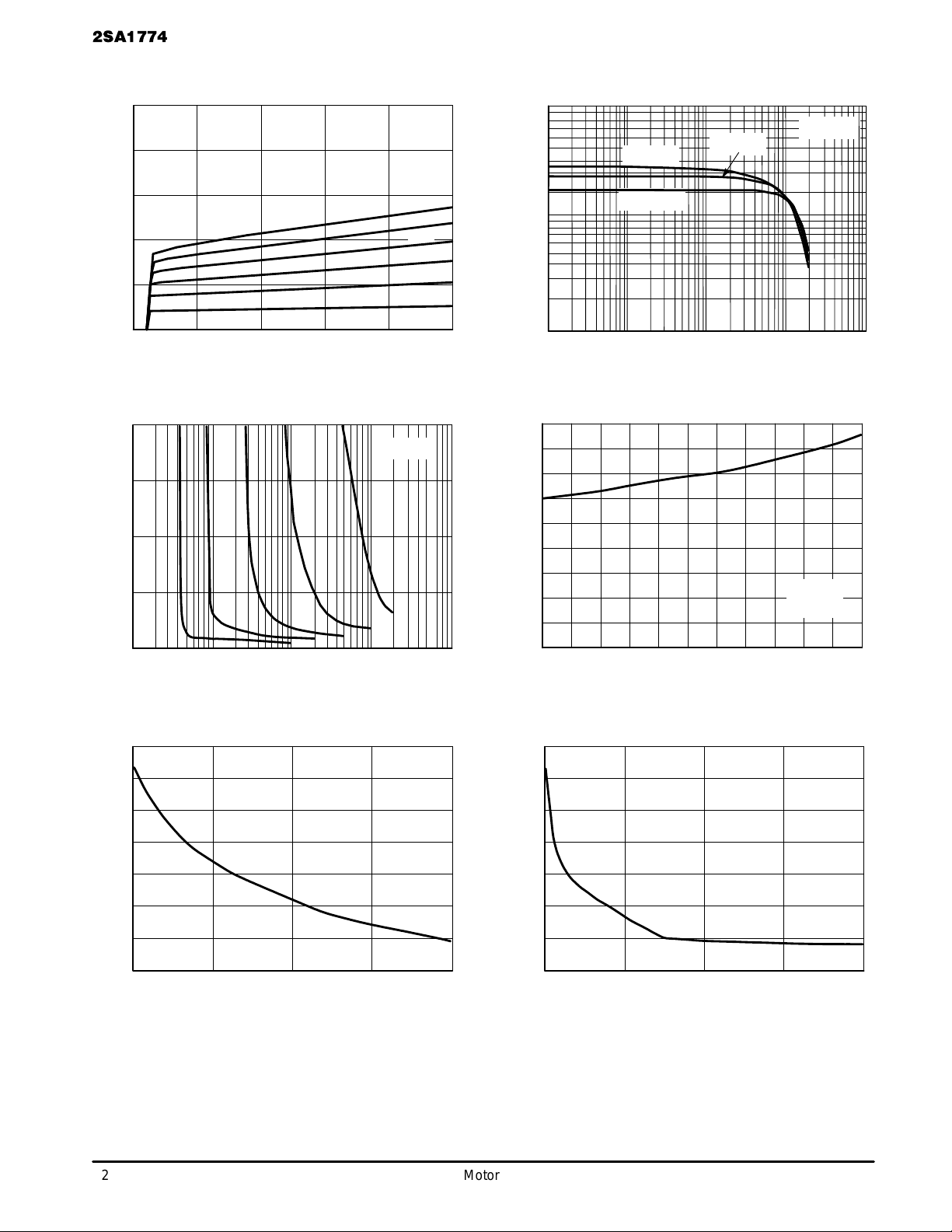
Figure 1. IC – V
0.1 1 10 100
IB, BASE CURRENT (mA)
CE
12
TA = 25°C
DC CURRENT GAIN
COLLECTOR VOLTAGE (mV)
TA = –25°C
100
10
0.1
1 10 100
IC, COLLECTOR CURRENT (mA)
Figure 2. DC Current Gain
900
800
700
600
500
400
300
200
100
0
0.5 1 5 10 20 40 60 80 100 150 200
0.2
IC, COLLECTOR CURRENT (mA)
TA = 25°C
VCE = 5 V
, INPUT CAP ACITANCE (pF)
ib
C
13
12
11
10
Figure 3. Collector Saturation Region
9
8
7
6
0
1234140
VEB (V)
Figure 5. Capacitance
12
10
, CAPACITANCE (pF)
ob
C
Figure 4. On Voltage
8
6
4
2
0
10 20 30 40
VCB (V)
Figure 6. Capacitance
2
Motorola Small–Signal Transistors, FETs and Diodes Device Data
 Loading...