

Motorola 2N7002LT1 Datasheet

SEMICONDUCTOR TECHNICAL DATA
Order this document
by 2N7002LT1/D
N–Channel Enhancement
1
GATE
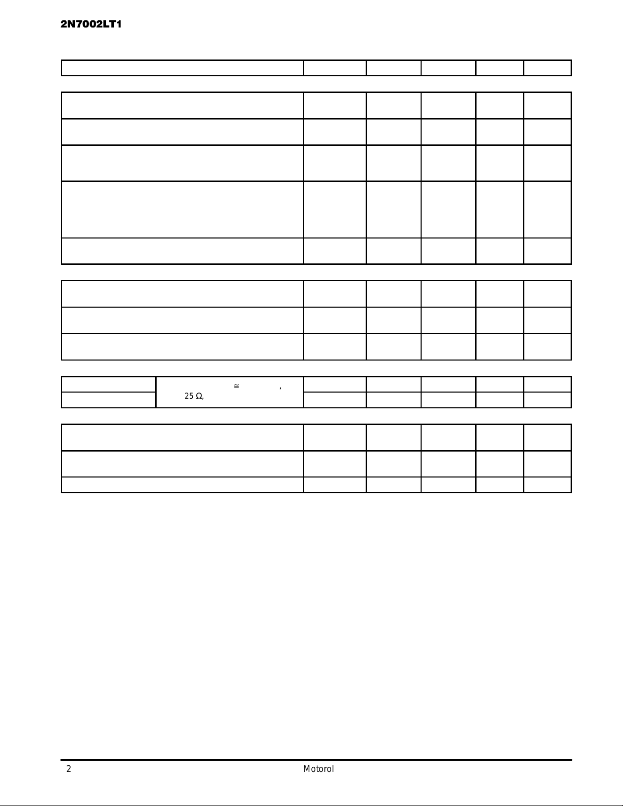
MAXIMUM RATINGS
Rating Symbol Value Unit
Drain–Source Voltage V
Drain–Gate Voltage (RGS = 1.0 MΩ) V
Drain Current — Continuous TC = 25°C
Drain Current — Continuous TC = 100°C
Drain Current — Pulsed
Gate–Source Voltage
— Continuous
— Non–repetitive (tp ≤ 50 µs)
(2)
(1)
(1)
I
V
V
DSS
DGR
I
D
I
D
DM
GS
GSM
THERMAL CHARACTERISTICS
Characteristic Symbol Max Unit
Total Device Dissipation FR–5 Board,
Derate above 25°C
Thermal Resistance, Junction to Ambient R
Total Device Dissipation
Alumina Substrate,
Derate above 25°C
Thermal Resistance, Junction to Ambient R
Junction and Storage Temperature TJ, T
(4)
TA = 25°C
(3)
TA = 25°C
DEVICE MARKING
2N7002L T1 = 702
60 Vdc
60 Vdc
±115
±75
±800
±20
±40
3 DRAIN
2 SOURCE
mAdc
Vdc
Vpk
P
D
θJA
P
D
θJA
stg
Motorola Preferred Device
3
1
2
CASE 318–08, STYLE 21
SOT–23 (TO–236AB)
225
1.8
556 °C/W
300
2.4
417 °C/W
–55 to +150 °C
mW
mW/°C
mW
mW/°C
ELECTRICAL CHARACTERISTICS (T
Characteristic
= 25°C unless otherwise noted)
A
Symbol Min Typ Max Unit
OFF CHARACTERISTICS
Drain–Source Breakdown Voltage
(VGS = 0, ID = 10 µAdc)
Zero Gate Voltage Drain Current TJ = 25°C
(VGS = 0, VDS = 60 Vdc) TJ = 125°C
Gate–Body Leakage Current, Forward
(VGS = 20 Vdc)
Gate–Body Leakage Current, Reverse
(VGS = –20 Vdc)
1. The Power Dissipation of the package may result in a lower continuous drain current.
2. Pulse Test: Pulse Width ≤ 300 µs, Duty Cycle ≤ 2.0%.
3. FR–5 = 1.0 x 0.75 x 0.062 in.
4. Alumina = 0.4 x 0.3 x 0.025 in 99.5% alumina.
Preferred devices are Motorola recommended choices for future use and best overall value.
REV 2
Motorola Small–Signal Transistors, FETs and Diodes Device Data
Motorola, Inc. 1997
V
(BR)DSS
I
DSS
I
GSSF
I
GSSR
60 — — Vdc
—
—
— — 100 nAdc
— — –100 nAdc
—
—
1.0
500
µAdc
1
2N7002LT1
(
DD
,
D
,
(T
ELECTRICAL CHARACTERISTICS
Characteristic
ON CHARACTERISTICS
Gate Threshold Voltage
(VDS = VGS, ID = 250 µAdc)
On–State Drain Current
(VDS ≥ 2.0 V
Static Drain–Source On–State Voltage
(VGS = 10 Vdc, ID = 500 mAdc)
(VGS = 5.0 Vdc, ID = 50 mAdc)
Static Drain–Source On–State Resistance
(VGS = 10 V, ID = 500 mAdc) TC = 25°C
(VGS = 5.0 Vdc, ID = 50 mAdc) TC = 25°C
Forward Transconductance
(VDS ≥ 2.0 V
DS(on)
DS(on)
(2)
, VGS = 10 Vdc)
, ID = 200 mAdc)
DYNAMIC CHARACTERISTICS
Input Capacitance
(VDS = 25 Vdc, VGS = 0, f = 1.0 MHz)
Output Capacitance
(VDS = 25 Vdc, VGS = 0, f = 1.0 MHz)
Reverse Transfer Capacitance
(VDS = 25 Vdc, VGS = 0, f = 1.0 MHz)
SWITCHING CHARACTERISTICS
Turn–On Delay Time
Turn–Off Delay Time
(VDD = 25 Vdc, ID ^ 500 mAdc,
RG = 25 Ω, RL = 50 Ω)
BODY–DRAIN DIODE RATINGS
Diode Forward On–Voltage
(IS = 11.5 mAdc, VGS = 0 V)
Source Current Continuous
(Body Diode)
Source Current Pulsed I
2. Pulse Test: Pulse Width ≤ 300 µs, Duty Cycle ≤ 2.0%.
= 25°C unless otherwise noted) (Continued)
A
TC = 125°C
TC = 125°C
(2)
Symbol Min Typ Max Unit
V
GS(th)
I
D(on)
V
DS(on)
r
DS(on)
g
C
C
C
t
d(on)
t
d(off)
V
I
SM
FS
iss
oss
rss
SD
S
1.0 — 2.5 Vdc
500 — — mA
—
—
—
—
—
—
80 — — mmhos
— — 50 pF
— — 25 pF
— — 5.0 pF
— — 30 ns
— — 40 ns
— — –1.5 Vdc
— — –115 mAdc
— — –800 mAdc
—
—
—
—
—
—
3.75
0.375
7.5
13.5
7.5
13.5
Vdc
Ohms
2
Motorola Small–Signal Transistors, FETs and Diodes Device Data
 Loading...