

3–12
Motorola Bipolar Power Transistor Device Data
. . . designed for medium–speed switching and amplifier applications. These devices
feature:
• Total Switching Time at 3 A typically 1.15 µs
• Gain Ranges Specified at 1 A and 3 A
• Low V
CE(sat)
: typically 0.5 V at IC = 5 A and IB = 0.5 A
• Excellent Safe Operating Areas
• Complement to 2N3791–92
MAXIMUM RATINGS
Rating
Symbol
2N3715
2N3716
ÎÎÎÎ
ÎÎÎÎ
ÎÎÎÎ
Unit
Collector–Emitter Voltage
V
CEO
60
80
ÎÎÎÎ
ÎÎÎÎ
ÎÎÎÎ
Volts
Collector–Base Voltage
V
CB
80
100
ÎÎÎÎ
ÎÎÎÎ
ÎÎÎÎ
Volts
Emitter–Base Voltage
V
EB
7.0
7.0
ÎÎÎÎ
ÎÎÎÎ
ÎÎÎÎ
Volts
Collector Current
I
C
10
10
ÎÎÎÎ
ÎÎÎÎ
ÎÎÎÎ
Amps
Base Current
I
B
4.0
4.0
ÎÎÎÎ
ÎÎÎÎ
ÎÎÎÎ
ÎÎÎÎ
Amps
Power Dissipation
P
D
150
150
ÎÎÎÎ
ÎÎÎÎ
ÎÎÎÎ
Watts
Thermal Resistance
θ
JC
1.17
1.17
ÎÎÎÎ
ÎÎÎÎ
ÎÎÎÎ
_
C/W
Operating Junction and Storage Temperature Range
TJ, T
stg
–65 to +200
ÎÎÎÎ
ÎÎÎÎ
ÎÎÎÎ
_
C
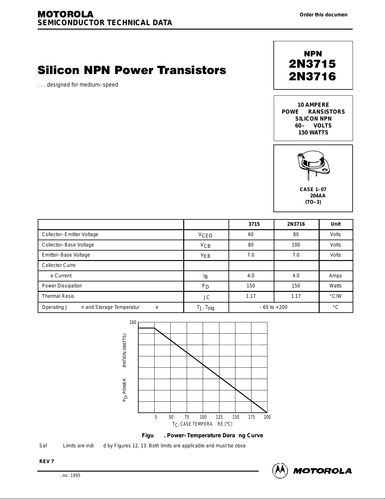
Safe Area Limits are indicated by Figures 12, 13. Both limits are applicable and must be observed.
140
120
100
80
60
40
0
20
0 25 50 75 100 125 150 175 200
Figure 1. Power–Temperature Derating Curve
TC, CASE TEMPERATURE (°C)
P
D
, POWER DISSIPATION (WATTS)
160
SEMICONDUCTOR TECHNICAL DATA
Order this document
by 2N3715/D
Motorola, Inc. 1995
10 AMPERE
POWER TRANSISTORS
SILICON NPN
60–80 VOLTS
150 WATTS
CASE 1–07
TO–204AA
(TO–3)
REV 7
3–13
Motorola Bipolar Power Transistor Device Data
ELECTRICAL CHARACTERISTICS (T
C
= 25_C unless otherwise noted)
Characteristic
ÎÎÎÎ
ÎÎÎÎ
ÎÎÎÎ
Symbol
Min
Max
ÎÎÎ
ÎÎÎ
ÎÎÎ
Unit
Emitter–Base Cutoff Current
(VEB = 7.0 Vdc) All Types
ÎÎÎÎ
ÎÎÎÎ
ÎÎÎÎ
ÎÎÎÎ
I
EBO
—
5.0
ÎÎÎ
ÎÎÎ
ÎÎÎ
ÎÎÎ
mAdc
Collector–Emitter Cutoff Current
(VCE = 80 Vdc, VBE = –1.5 Vdc) 2N3715
(VCE = 100 Vdc, VBE = –1.5 Vdc) 2N3716
(VCE = 60 Vdc, VBE = –1.5 Vdc, TC = 150_C) 2N3715
(VCE = 80 Vdc, VBE = –1.5 Vdc, TC = 150_C) 2N3716
ÎÎÎÎ
ÎÎÎÎ
ÎÎÎÎ
ÎÎÎÎ
ÎÎÎÎ
ÎÎÎÎ
I
CEX
—
—
—
—
1.0
1.0
10
10
ÎÎÎ
ÎÎÎ
ÎÎÎ
ÎÎÎ
ÎÎÎ
ÎÎÎ
mAdc
Collector–Emitter Sustaining Voltage (1)
(IC = 200 mAdc, IB = 0) 2N3715
2N3716
ÎÎÎÎ
ÎÎÎÎ
ÎÎÎÎ
ÎÎÎÎ
V
CEO(sus)
*
60
80
—
—
ÎÎÎ
ÎÎÎ
ÎÎÎ
ÎÎÎ
Vdc
DC Current Gain (1)
(IC = 1.0 Adc, VCE = 2.0 Vdc) 2N3715, 2N3716
(IC = 3.0 Adc, VCE = 2.0 Vdc) 2N3715, 2N3716
ÎÎÎÎ
ÎÎÎÎ
ÎÎÎÎ
ÎÎÎÎ
ÎÎÎÎ
hFE*
50
30
150
—
ÎÎÎ
ÎÎÎ
ÎÎÎ
ÎÎÎ
ÎÎÎ
—
Collector–Emitter Saturation Voltage (1)
(IC = 5.0 Adc, IB = 0.5 Adc) 2N3715, 2N3716
ÎÎÎÎ
ÎÎÎÎ
ÎÎÎÎ
V
CE(sat)
*
—
0.8
ÎÎÎ
ÎÎÎ
ÎÎÎ
Vdc
Base–Emitter Saturation Voltage (1)
(IC = 5.0 Adc, IB = 0.5 Adc) 2N3715, 2N3716
ÎÎÎÎ
ÎÎÎÎ
ÎÎÎÎ
ÎÎÎÎ
V
BE(sat)
*
—
1.5
ÎÎÎ
ÎÎÎ
ÎÎÎ
ÎÎÎ
Vdc
Base–Emitter Voltage (1)
(IC = 3.0 Adc, VCE = 2.0 Vdc) All Types
ÎÎÎÎ
ÎÎÎÎ
ÎÎÎÎ
ÎÎÎÎ
VBE*
—
1.5
ÎÎÎ
ÎÎÎ
ÎÎÎ
ÎÎÎ
Vdc
Small Signal Current Gain
(VCE = 10 Vdc, IC = 0.5 Adc, f = 1.0 MHz) All Types
ÎÎÎÎ
ÎÎÎÎ
ÎÎÎÎ
ÎÎÎÎ
h
fe
4.0
—
ÎÎÎ
ÎÎÎ
ÎÎÎ
ÎÎÎ
—
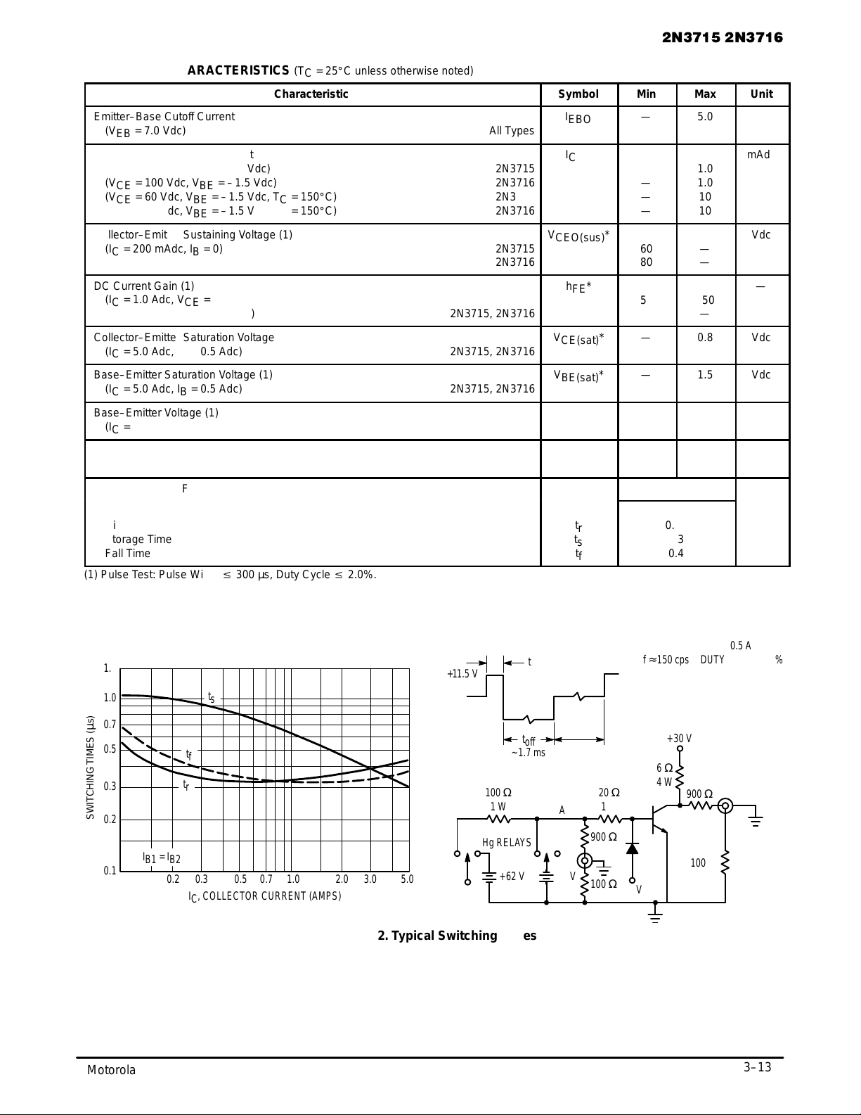
Switching Times (Figure 2)
ÎÎÎÎ
ÎÎÎÎ
ÎÎÎÎ
Typ
ÎÎÎ
ÎÎÎ
ÎÎÎ
µs
(IC = 5.0 A, IB1 = IB2 = 0.5 Adc)
Rise Time
Storage Time
Fall Time
ÎÎÎÎ
ÎÎÎÎ
ÎÎÎÎ
ÎÎÎÎ
ÎÎÎÎ
t
r
t
s
t
f
0.45
0.3
0.4
ÎÎÎ
ÎÎÎ
ÎÎÎ
ÎÎÎ
ÎÎÎ
(1) Pulse Test: Pulse Width v 300 µs, Duty Cycle v 2.0%.
1.5
0.1
Figure 2. Typical Switching Times
IC, COLLECTOR CURRENT (AMPS)
1.0
0.7
0.5
0.3
0.2
0.1
0.2 0.3 0.5 0.7 1.0 2.0 3.0 5.0
SWITCHING TIMES ( s)
µ
t
s
t
f
t
r
IB1 = I
B2
+11.5 V
ton ~ 30 µs
–9 V
TEST CIRCUIT
~4.8 ms
WAVE SHAPE
AT POINT A
IC = 5 A, IB1 = IB2 = 0.5 A
f
≈
150 cps DUTY CYCLE ≈ 2%
+30 V
6
Ω
4 W
900
Ω
100
Ω
–4 V
900
Ω
100
Ω
1 W
20
Ω
1 W
A
Hg RELAYS
+62 V –9 V
100
Ω
t
off
~1.7 ms

3–14
Motorola Bipolar Power Transistor Device Data
10
0.1
Figure 3. Collector Current versus Base Current
IB, BASE CURRENT (mA)
7.0
5.0
3.0
2.0
1.0
0.07
0.05
0.01
0.2 0.5 1.0 5.0 20 50 100 1000200
0.03
0.02
I
C
, COLLECTOR CURRENT (AMPS)
TJ = 175°C
2.0 10 500
–40°C
VCE = 2 V
SEE NOTES 1, 2
25°C
2N3715, 2N3716
1000
0
Figure 4. Base Current–Voltage Variations
VBE, BASE–EMITTER VOLTAGE (VOLTS)
700
1.0
0.4 0.8 1.6 2.0
I
B
, BASE CURRENT (mA)
TJ = 175°C
1.2
–40°C
VCE = 2 V
SEE NOTE 2
25°C
500
300
200
100
70
50
30
20
10
7.0
5.0
3.0
2.0
10
0.1
Figure 5. Collector Current–Voltage Variations
VBE, BASE–EMITTER VOLTAGE (VOLTS)
7
5
3
2
1
0.7
0.5
0.1
0.4 1.6 2.0
0.3
0.2
I
C
, COLLECTOR CURRENT (AMPS)
TJ = 175°C
0.8 1.2
–40°C
25°C
2N3715, 2N3716
VCE = 2 V
SEE NOTE 2
0.1
0.2
0.3
0.5
0.7
NOTE 1. Dotted line indicates metered base current plus the I
CBO
of the transistor at 175_C.
NOTE 2. Pulse test: pulse width ≈ 200 µsec, duty cycle ≈ 1.5%.

3–15
Motorola Bipolar Power Transistor Device Data
Figure 6. Collector–Emitter Saturation Voltage Variations
IB, BASE CURRENT (mA)
1.4
0.1
10
1.2
1.0
0.8
0.6
0.4
0.2
20 30 50 70 100 200 300 500 700 1000 2000
V
CE(sat)
, COLLECTOR–EMITTER SATURATION
VOLTAGE (VOLTS)
TJ =
25
°
C
–40
°
C
175
°
C
SEE NOTE 2
IC = 5 A
Figure 7. Base–Emitter Saturation Voltage Variations
IB, BASE CURRENT (mA)
1.4
0.1
10
1.2
1.0
0.8
0.6
0.4
0.2
20 30 50 70 100 200 300 500 700 1000 2000
V
BE(sat)
, BASE–EMITTER SATURATION
VOLTAGE (VOLTS)
10
Figure 8. Collector Current versus
Base–Emitter Voltage
VBE, BASE–EMITTER VOLTAGE (VOLTS)
, COLLECTOR CURRENT (mA)I
C
0.1
–0.6 –0.4 –0.2 0 0.2 0.4
TJ = 175°C
REVERSE
FORWARD
7.0
5.0
3.0
2.0
1.0
0.7
0.5
0.3
0.2
TJ = 100°C
VCE = V
CEO
– 20 V
SEE NOTE 2
100
Figure 9. Collector Current versus
Base–Emitter Resistance
RBE, EXTERNAL BASE–EMITTER RESISTANCE (OHMS)
, COLLECTOR CURRENT (mA)I
C
0.1
1 10 100 1000 10,000 100,000
50
30
20
10
5.0
3.0
2.0
1.0
0.5
0.3
0.2
IC = 3 A
IC = 1 A
IC = 5 A
IC = 3 A
IC = 1 A
TJ =
25
°
C
–40
°
C
175
°
C
SEE NOTE 2
VCE = V
CEO
– 20 V
SEE NOTE 2
TJ = 175°C
TJ = 100°C

3–16
Motorola Bipolar Power Transistor Device Data
Figure 10. Current Gain Variations
IC, COLLECTOR CURRENT (AMPS)
0
0.01
200
150
100
50
0.02 0.03 0.05 0.07 0.1 0.2 0.3 0.5 0.7 1.0 102.0 3.0 5.0 7.0
TJ = 175°C
–40°C
VCE = 2 V
25°C
h
FE
+
IC– I
CBO
I
B
)
I
CBO
Figure 11. Current Gain — Bandwidth Product versus Collector Current
IC, COLLECTOR CURRENT (AMPS)
0
0.1
8
6
4
2
0.2 0.3 0.5 0.7 1.0 2.0 3.0 5.0
VCE = 6 V
f , CURRENT GAIN — BANDWIDTH PRODUCT (mc)
τ
h
FE
, CURRENT GAIN
10
0
Figure 12. 2N3715
VCE, COLLECTOR–EMITTER VOLTAGE (VOLTS)
7
5
3
2
1
0.7
0.5
0.1
10 20 30 40 50 60 70
0.3
0.2
I
C
, COLLECTOR CURRENT (AMPS)
DC to 5 ms
500 µs
250 µs
10
0
Figure 13. 2N3716
VCE, COLLECTOR–EMITTER VOLTAGE (VOLTS)
7
5
3
2
1
0.7
0.5
0.1
10 20 30 40 50 60 70
0.3
0.2
I
C
, COLLECTOR CURRENT (AMPS)
500 µs
250 µs
≤
50 µs
SAFE OPERATING AREAS
80 90
DC to 5 ms
1 ms
≤
50 µs
1 ms
The Safe Operating Area Curves indicate IC – VCE limits
below which the device will not go into secondary breakdown. Collector load lines for specific circuits must fall within
the applicable Safe Area to avoid causing a collector–emitter
short. (Duty cycle of the excursions make no significant
change in these safe areas.) To insure operation below the
maximum TJ, the power–temperature derating curve must be
observed for both steady state and pulse power conditions.

3–17
Motorola Bipolar Power Transistor Device Data
PACKAGE DIMENSIONS
NOTES:
1. DIMENSIONING AND TOLERANCING PER ANSI
Y14.5M, 1982.
2. CONTROLLING DIMENSION: INCH.
3. ALL RULES AND NOTES ASSOCIATED WITH
REFERENCED TO–204AA OUTLINE SHALL APPLY.
STYLE 1:
PIN 1. BASE
2. EMITTER
CASE: COLLECTOR
DIM MIN MAX MIN MAX
MILLIMETERSINCHES
A 1.550 REF 39.37 REF
B ––– 1.050 ––– 26.67
C 0.250 0.335 6.35 8.51
D 0.038 0.043 0.97 1.09
E 0.055 0.070 1.40 1.77
G 0.430 BSC 10.92 BSC
H 0.215 BSC 5.46 BSC
K 0.440 0.480 11.18 12.19
L 0.665 BSC 16.89 BSC
N ––– 0.830 ––– 21.08
Q 0.151 0.165 3.84 4.19
U 1.187 BSC 30.15 BSC
V 0.131 0.188 3.33 4.77
A
N
E
C
K
–T–
SEATING
PLANE
2 PLD
M
Q
M
0.13 (0.005) Y
M
T
M
Y
M
0.13 (0.005) T
–Q–
–Y–
2
1
U
L
G
B
V
H
CASE 1–07
TO–204AA (TO–3)
ISSUE Z
How to reach us:
USA /EUROPE: Motorola Literature Distribution; JAPAN: Nippon Motorola Ltd.; Tatsumi–SPD–JLDC, Toshikatsu Otsuki,
P.O. Box 20912; Phoenix, Arizona 85036. 1–800–441–2447 6F Seibu–Butsuryu–Center, 3–14–2 Tatsumi Koto–Ku, Tokyo 135, Japan. 03–3521–8315
MFAX: RMFAX0@email.sps.mot.com – TOUCHTONE (602) 244–6609 HONG KONG: Motorola Semiconductors H.K. Ltd.; 8B Tai Ping Industrial Park,
INTERNET: http://Design–NET.com 51 Ting Kok Road, Tai Po, N.T., Hong Kong. 852–26629298
Motorola reserves the right to make changes without further notice to any products herein. Motorola makes no warranty , representation or guarantee regarding
the suitability of its products for any particular purpose, nor does Motorola assume any liability arising out of the application or use of any product or circuit,
and specifically disclaims any and all liability, including without limitation consequential or incidental damages. “T ypical” parameters can and do vary in different
applications. All operating parameters, including “T ypicals” must be validated for each customer application by customer’s technical experts. Motorola does
not convey any license under its patent rights nor the rights of others. Motorola products are not designed, intended, or authorized for use as components in
systems intended for surgical implant into the body, or other applications intended to support or sustain life, or for any other application in which the failure of
the Motorola product could create a situation where personal injury or death may occur. Should Buyer purchase or use Motorola products for any such
unintended or unauthorized application, Buyer shall indemnify and hold Motorola and its officers, employees, subsidiaries, affiliates, and distributors harmless
against all claims, costs, damages, and expenses, and reasonable attorney fees arising out of, directly or indirectly, any claim of personal injury or death
associated with such unintended or unauthorized use, even if such claim alleges that Motorola was negligent regarding the design or manufacture of the part.
Motorola and are registered trademarks of Motorola, Inc. Motorola, Inc. is an Equal Opportunity/Affirmative Action Employer.
2N3715/D
*2N3715/D*
◊
 Loading...