

Page 1
SR3 Type 1 Technical Manual TSP005.doc Issue 5.0 – Jan 2005
This document is the copyright of Money Controls Ltd and may not be reproduced in part or in total by any means,
electronic or otherwise, without the written permission of Money Controls Ltd. Money Controls Ltd does not accept
liability for any errors or omissions contained within this document. Money Controls Ltd shall not incur any
penalties arising out of the adherence to, interpretation of, or reliance on, this standard. Money Controls Ltd will
provide full support for this product when used as described within this document. Use in applications not covered
or outside the scope of this document may not be supported. Money Controls Ltd. reserves the right to amend,
improve or change the product referred to within this document or the document itself at any time.
Money Controls 2005. All rights reserved.
Page 2

SR3 Type 1 Technical Manual TSP005.doc Issue 5.0 – Jan 2005
Contents
1. Diary of Changes ........................................................................................................................................... 5
2. Introduction.................................................................................................................................................... 6
3. Mechanical Configuration............................................................................................................................. 7
4. Rear Cover Details....................................................................................................................................... 10
5. Parallel Interface.......................................................................................................................................... 11
5.1 Inhibit All ................................................................................................................................................ 11
5.2 Coin Accept Outputs.............................................................................................................................. 12
5.3 Reject .................................................................................................................................................... 12
6. Credit Codes ................................................................................................................................................ 13
6.1 Standard Parallel Credit Codes ............................................................................................................. 13
6.2 Standard Binary Credit Codes ............................................................................................................... 13
7. Debug Features ........................................................................................................................................... 14
8. DIL Switch Options...................................................................................................................................... 15
9. Accept and Inhibit Configuration............................................................................................................... 16
9.1 To Inhibit Specific Coins ........................................................................................................................ 16
9.2 To Enable Specific Coins....................................................................................................................... 16
10. Bank Select .............................................................................................................................................. 17
10.1 Both Banks ON...................................................................................................................................... 17
10.2 Bank 1 ON Bank 2 OFF......................................................................................................................... 17
10.3 Bank 1 OFF Bank 2 ON......................................................................................................................... 17
11. Teach and Run™ Option......................................................................................................................... 18
11.1 Programming Steps ............................................................................................................................... 18
11.2 BANK 1.................................................................................................................................................. 19
11.3 BANK 2.................................................................................................................................................. 19
12. Erase All Windows .................................................................................................................................. 20
13. Adjustable Coin Security ........................................................................................................................ 21
13.1 Decrease Security ................................................................................................................................. 22
13.2 Increase Security ................................................................................................................................... 22
13.3 Reset Security ....................................................................................................................................... 22
14. Alarms ...................................................................................................................................................... 23
14.1 Enable ................................................................................................................................................... 23
14.2 Disable................................................................................................................................................... 23
15. Diagnostics (power-up)........................................................................................................................... 24
16. Sorter Option ........................................................................................................................................... 24
16.1 Sorter Mode 1 (default).......................................................................................................................... 24
16.2 Sorter Mode 2........................................................................................................................................ 24
16.3 Sorter Mode 3........................................................................................................................................ 24
17. Sorter Drivers........................................................................................................................................... 25
17.1 Sorter Drive Circuit ................................................................................................................................ 25
17.11 Theory of operation........................................................................................................................ 25
17.2 Sorter Drive Examples........................................................................................................................... 26
17.3 Sort Outputs v Sorter Paths................................................................................................................... 26
18. Totaliser Mode ......................................................................................................................................... 27
18.1 19 way Parallel Interface Connector...................................................................................................... 27
18.2 CMETER ............................................................................................................................................... 28
18.3 Player 1 HI / Player 1 LO ....................................................................................................................... 29
18.4 Player 2 to 4 .......................................................................................................................................... 29
18.5 Dispense 1 to 4...................................................................................................................................... 30
19. Totalising Options ................................................................................................................................... 31
19.1 Set a Game Price .................................................................................................................................. 31
19.2 Set Bonus Level 1.................................................................................................................................. 32
19.3 Set Bonus Level 2.................................................................................................................................. 32
19.4 Set Bonus Award Level 1 ...................................................................................................................... 33
19.5 Set Bonus Award Level 2 ...................................................................................................................... 33
19.6 Test Credit Mode ................................................................................................................................... 34
19.7 Summary of Totalising Functions........................................................................................................... 35
20. Totalising Parameters ............................................................................................................................. 36
21. Coin Dimensions ..................................................................................................................................... 37
22. Label Details Explained........................................................................................................................... 38
Money Controls 2005. All rights reserved.
Page 2 of 50
Page 3

SR3 Type 1 Technical Manual TSP005.doc Issue 5.0 – Jan 2005
23. Protocols .................................................................................................................................................. 39
23.1 Serial Interface ...................................................................................................................................... 39
24. ccTalk Serial Messages.......................................................................................................................... 40
25. ccTalk Interface Circuits ......................................................................................................................... 42
25.1 Circuit 1 – ccTalk Standard Interface..................................................................................................... 42
25.2 Circuit 2 – ccTalk Low Cost Interface .................................................................................................... 43
25.3 Circuit 3 – ccTalk Direct Interface.......................................................................................................... 44
25.4 Circuit 4 – ccTalk PC Interface .............................................................................................................. 45
26. Fault Finding ............................................................................................................................................ 46
27. Service...................................................................................................................................................... 47
28. Electrical Interface Requirements.......................................................................................................... 47
29. Specified EMC Performance................................................................................................................... 48
29.1 Emissions .............................................................................................................................................. 48
29.2 Immunity ................................................................................................................................................ 48
29.3 Shock / Vibration Immunity .................................................................................................................... 48
30. Appendix A – Available Parallel Interface Looms................................................................................. 49
Tables
Table 1: SR3 Rear Cover Details. ......................................................................................................................... 10
Table 2: Parallel Interface...................................................................................................................................... 11
Table 3: Debug Features ....................................................................................................................................... 14
Table 4: DIL Switch Functions............................................................................................................................... 15
Table 5: SR3 DIL Switch Guide ............................................................................................................................. 15
Table 6: Teach and Run™ Programming - Bank 1............................................................................................... 19
Table 7: Teach and Run™ Programming - Bank 2............................................................................................... 19
Table 8: DIL Switches - Decrease Security ........................................................................................................... 22
Table 9: DIL Switches - Increase Security............................................................................................................. 22
Table 10: Sort Outputs v Sorter Paths................................................................................................................... 26
Table 11: 19 way Parallel Interface Connector ...................................................................................................... 27
Table 12: SR3 Totalising DIL Switch Guide........................................................................................................... 31
Table 13: Totalising Parameters............................................................................................................................ 36
Table 14: ccTalk Serial Commands ..................................................................................................................... 40
Table 15: Error Codes ........................................................................................................................................... 41
Table 16: Fault Codes ........................................................................................................................................... 41
Table 17: Status Codes ......................................................................................................................................... 41
Table 18: Power Supply ........................................................................................................................................ 47
Table 19: Current Consumption............................................................................................................................. 47
Table 20: Environmental Ranges .......................................................................................................................... 47
Table 21: Available Parallel Interface Looms......................................................................................................... 49
Money Controls 2005. All rights reserved.
Page 3 of 50
Page 4

SR3 Type 1 Technical Manual TSP005.doc Issue 5.0 – Jan 2005
Figures
Figure 1: Accept and Reject Paths .......................................................................................................................... 7
Figure 2: Front Plate Model Details ......................................................................................................................... 8
Figure 3: Front Plate Cut-out Details ....................................................................................................................... 8
Figure 4: Standard Model Details ............................................................................................................................ 9
Figure 5: Reverse Model Details ............................................................................................................................. 9
Figure 6: SR3 Connector Side............................................................................................................................... 10
Figure 7: SR3 Parallel Connector .......................................................................................................................... 11
Figure 8: Coin Accept Outputs............................................................................................................................... 12
Figure 9: Reject Operated Output.......................................................................................................................... 12
Figure 10: Sort Output Connector Details.............................................................................................................. 25
Figure 11: Sorter Drive Output Circuit ................................................................................................................... 25
Figure 12: Sorter Drive Examples.......................................................................................................................... 26
Figure 13: CMETER Output .................................................................................................................................. 28
Figure 14: Player 1 HI / Player 1 LO Output .......................................................................................................... 29
Figure 15: Player 2 to 4 Outputs............................................................................................................................ 29
Figure 16: Dispense 1 to 4 Inputs.......................................................................................................................... 30
Figure 17: SR3 Accepted Coin Dimensions Graph................................................................................................ 37
Figure 18: ccTalk Serial Connector....................................................................................................................... 39
Figure 19: Circuit 1, ccTalk Standard Interface..................................................................................................... 42
Figure 20: Circuit 2, ccTalk Low Cost Interface .................................................................................................... 43
Figure 21: Circuit 3, ccTalk Direct Interface.......................................................................................................... 44
Figure 22: Circuit 4, ccTalk PC Interface .............................................................................................................. 45
Money Controls 2005. All rights reserved.
Page 4 of 50
Page 5

SR3 Type 1 Technical Manual TSP005.doc Issue 5.0 – Jan 2005
1. Diary of Changes
Issue 2.0................................................................................................................September 2000
Issue 3.0................................................................................................................ 29
th
March 2002
¾ Title changed to SR3 Type 1
¾ Added credit code details
¾ Added label description
¾ Output diagrams added
¾ Totaliser option added
¾ Fault finding table added
¾ Sorter option added
¾ ccTalk headers and circuits added
¾ Power-up Diagnostics added
¾ Re-ordered headings
¾ Amended last page disclaimer
¾ Table references on page 14 corrected
¾ Table references on page 17 corrected
¾ Section references on page 17 corrected
¾ Table references on page 19 corrected
¾ Erase all windows MechTool
TM
option added
¾ Dimensional information added
¾ Applied TMWP V3.0
¾ Pictures changed to .jpg
¾ Added section on available interface looms
Issue 4.0................................................................................................................... 26
th
April 2002
¾ Added Figure 7: SR3 Parallel Connector
¾ Added switch drawings for visual indication
Issue 4.1..................................................................................................................... 6
¾ Modification to disclaimer.
Issue 4.2.................................................................................................................... 18
¾ Typing error in section 5.3 Pin 6 changed to Pin 5
¾ Applied TMWP V3.2
¾ Changed the ‘high’ voltage of Inhibit All.
Issue 4.3...................................................................................................................... 6
¾ Changed ccTalk
®
to ccTalk throughout the document.
Issue 4.4...................................................................................................................30
¾ Changed footer
Issue 5.0.....................................................................................................................13
¾ Improved section 17 “Sorter Drivers”.
¾ Changed links for Figure 1 to Figure 6
.
th
Sept 2002
th
Feb 2003
th
Aug 2003
th
June 2004
th
Jan 2005
Money Controls 2005. All rights reserved.
Page 5 of 50
Page 6

SR3 Type 1 Technical Manual TSP005.doc Issue 5.0 – Jan 2005
2. Introduction
The SR3 series of coin acceptors has been designed to be compatible with the standard 3.5”
mechanical and electronic acceptors currently used throughout the vending, amusement and
leisure industries.
Through the development of Series Resonance Technology, the SR3 incorporates the highest
levels of discrimination and functionality. Each acceptor within the series will accept up to 12
different coins from 15mm – 31mm in diameter.
The SR3 can be programmed on site without the use of coins using “ccProgrammer”, or using
a ccTeach programmer but for total flexibility, if a new coin/token is required, the Teach and
Run function can be used.
The SR3 Type1 has the option to attach an external totaliser PCB and has the capability to
drive an external sorter.
Money Controls 2005. All rights reserved.
Page 6 of 50
Page 7
SR3 Type 1 Technical Manual TSP005.doc Issue 5.0 – Jan 2005
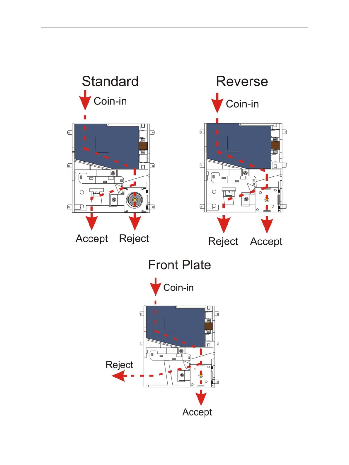
3. Mechanical Configuration
Figure 1: Accept and Reject Paths
Money Controls 2005. All rights reserved.
Page 7 of 50
Page 8
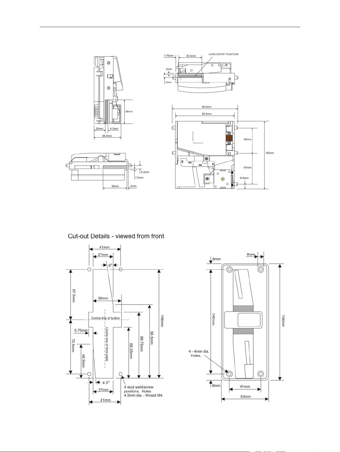
SR3 Type 1 Technical Manual TSP005.doc Issue 5.0 – Jan 2005
Figure 2: Front Plate Model Details
Figure 3: Front Plate Cut-out Details
Money Controls 2005. All rights reserved.
Page 8 of 50
Page 9
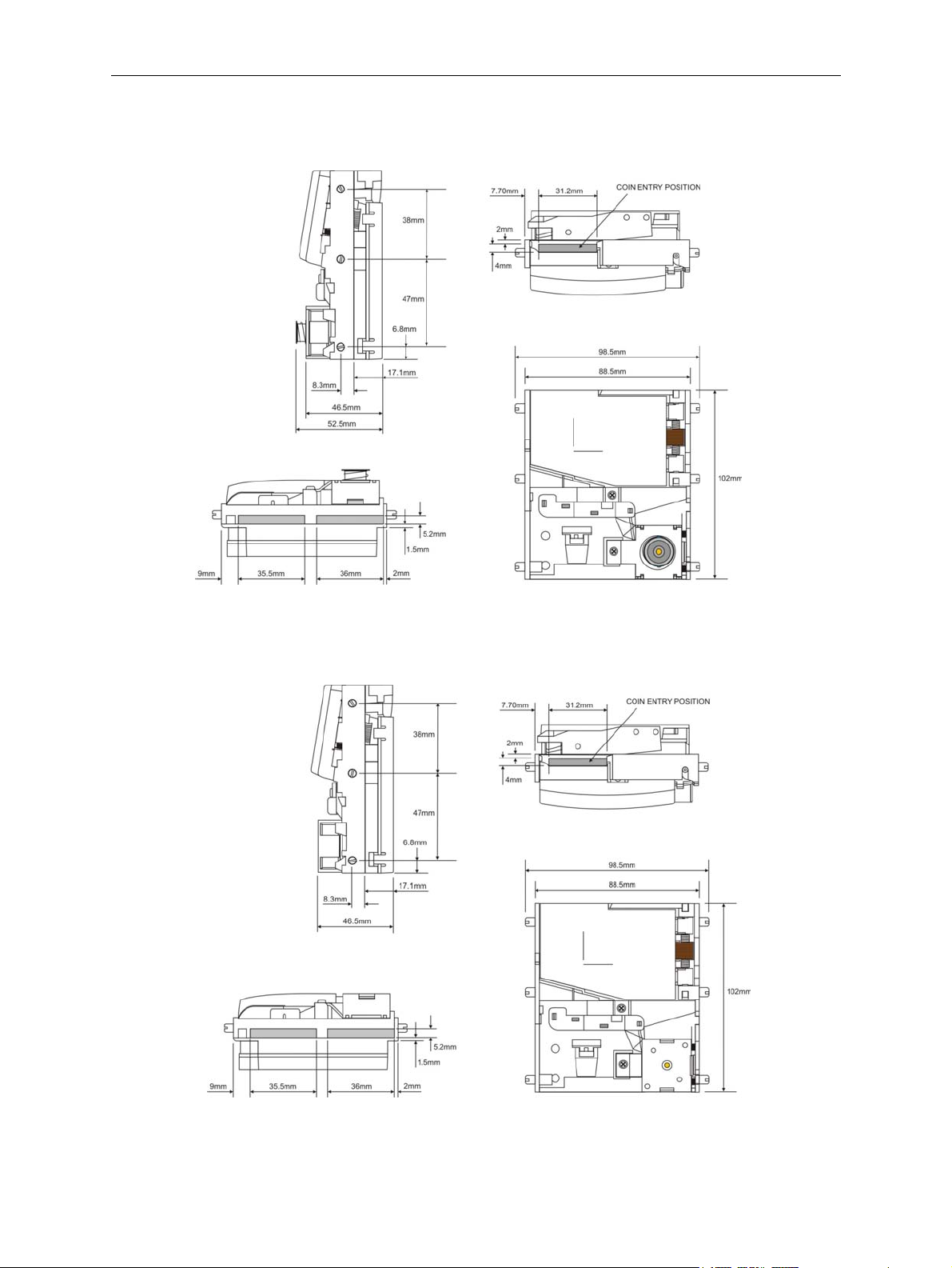
SR3 Type 1 Technical Manual TSP005.doc Issue 5.0 – Jan 2005
Figure 4: Standard Model Details
Figure 5: Reverse Model Details
Money Controls 2005. All rights reserved.
Page 9 of 50
Page 10
SR3 Type 1 Technical Manual TSP005.doc Issue 5.0 – Jan 2005
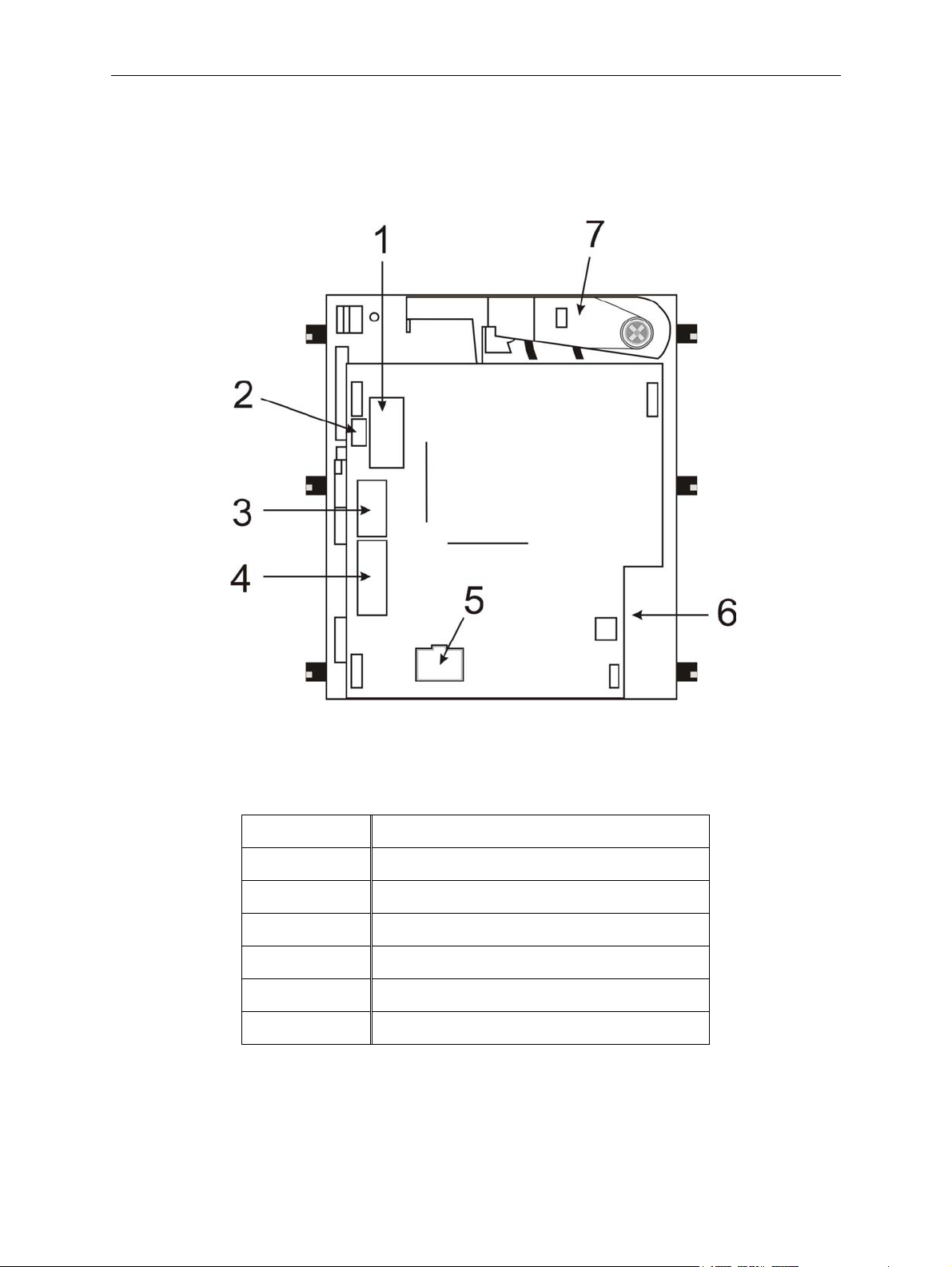
4. Rear Cover Details
Figure 6: SR3 Connector Side
Table 1: SR3 Rear Cover Details.
1 Option Switches
2LED
3 Serial Interface (ccTalk)
4 Sorter Connector
5 Totaliser Connector
6 Parallel Connector
7 Reject Lever
Money Controls 2005. All rights reserved.
Page 10 of 50
Page 11
SR3 Type 1 Technical Manual TSP005.doc Issue 5.0 – Jan 2005
5. Parallel Interface
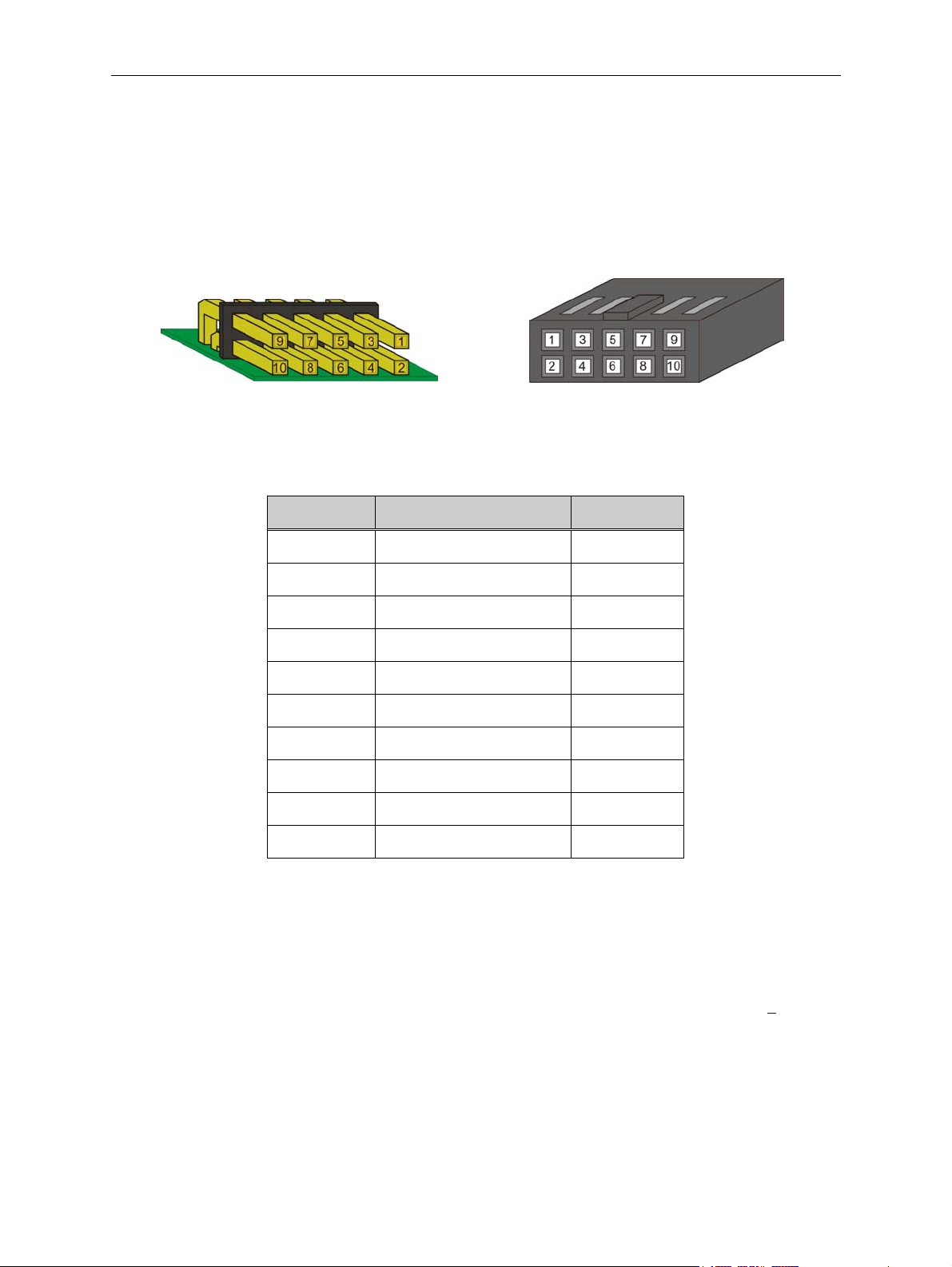
Figure 7: SR3 Parallel Connector
Industry standard interface.
Connector type: 10 pin DIL
Table 2: Parallel Interface
PIN FUNCTION ACTIVE
5.1 Inhibit All
When the input on pin 6 on the 10 way connector is high (>1.2 volts), all the coins will be
rejected.
The Inhibit All pin has to be low (<1.2 volts) or not connected, in order for those coins not
individually inhibited, determined by the programmed settings (See section 9), to be
accepted.
10 VOLTS
2 + SUPPLY
3 Accept 5 Low
4 Accept 6 Low
5 Reject operated Low
6 Inhibit All
7 Accept 1 Low
8 Accept 2 Low
9 Accept 3 Low
10 Accept 4 Low
(Default Accept)
High
If no coins are individually inhibited and both banks are enabled, then ALL coins will be
accepted.
Money Controls 2005. All rights reserved.
Page 11 of 50
Page 12
SR3 Type 1 Technical Manual TSP005.doc Issue 5.0 – Jan 2005
5.2 Coin Accept Outputs
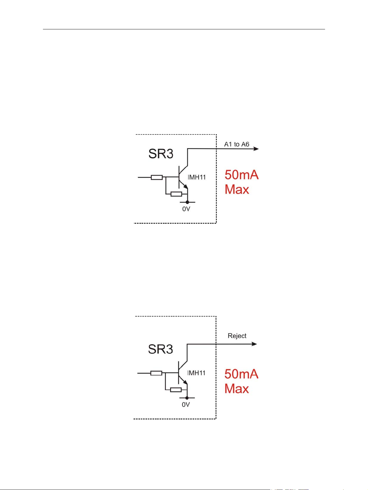
Each coin accept output consists of an open collector NPN transistor. On acceptance of a
true coin the transistor is turned on for a period of 100ms (+/- 20%) to less than 0.7 volts at a
Max. 50mA. The host machine must look for valid credit pulses NOT LESS THAN 50ms. It is
not sufficient to merely detect the edges of credit pulses. This ‘debounce’ will prevent credits
being registered by the host machine as a result of any noise or false credit pulses being
induced on the output lines.
Figure 8: Coin Accept Outputs
5.3 Reject
Each time the reject lever is pressed, a lug on the reject lever breaks an optical beam,
situated on the PCB. This is read by the processor and an output signal is sent to pin 5
(reject operated) on the parallel connector.
This output will remain active for as long as the reject lever is pressed, to less than 0.7 volts
at a Max. 50mA.
Figure 9: Reject Operated Output
Money Controls 2005. All rights reserved.
Page 12 of 50
Page 13
SR3 Type 1 Technical Manual TSP005.doc Issue 5.0 – Jan 2005
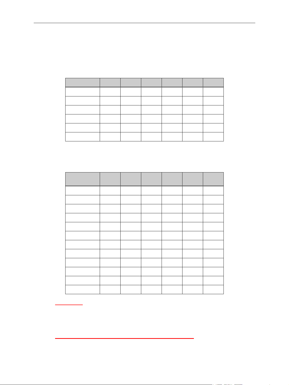
6. Credit Codes
6.1 Standard Parallel Credit Codes
This is the basic 6 coin pattern, one output is active per coin and the output corresponds to
the coin position. Coins 7 to 12 are the same codes as coins 1 to 6.
Coin No. A6 A5 A4 A3 A2 A1
Coin 1, 7000001
Coin 2, 8000010
Coin 3, 9000100
Coin 4, 10001000
Coin 5, 11010000
Coin 6, 12100000
6.2 Standard Binary Credit Codes
This pattern shows A4 as a strobe. This can be used as a check whereby the credit codes
are only looked at and valid when A4 is active.
Strobe
Coin No. A6 A5
Coin 1
Coin 2
Coin 3
Coin 4
Coin 5
Coin 6
Coin 7
Coin 8
Coin 9
Coin 10
Coin 11
Coin 12
Please Note: Either Parallel or Binary must be selected when ordering.
You CANNOT switch between Binary and Parallel on the SR3 without re-programming.
001000
001001
001010
001011
001100
001101
001110
001111
011000
011001
011010
011011
A4 A3 A2 A1
Also, these are the standard available codes.
You can select different combinations of credits to suit your application.
A1 to A6 ALL ON is NOT available – this is the ALARM code.
Money Controls 2005. All rights reserved.
Page 13 of 50
Page 14
SR3 Type 1 Technical Manual TSP005.doc Issue 5.0 – Jan 2005
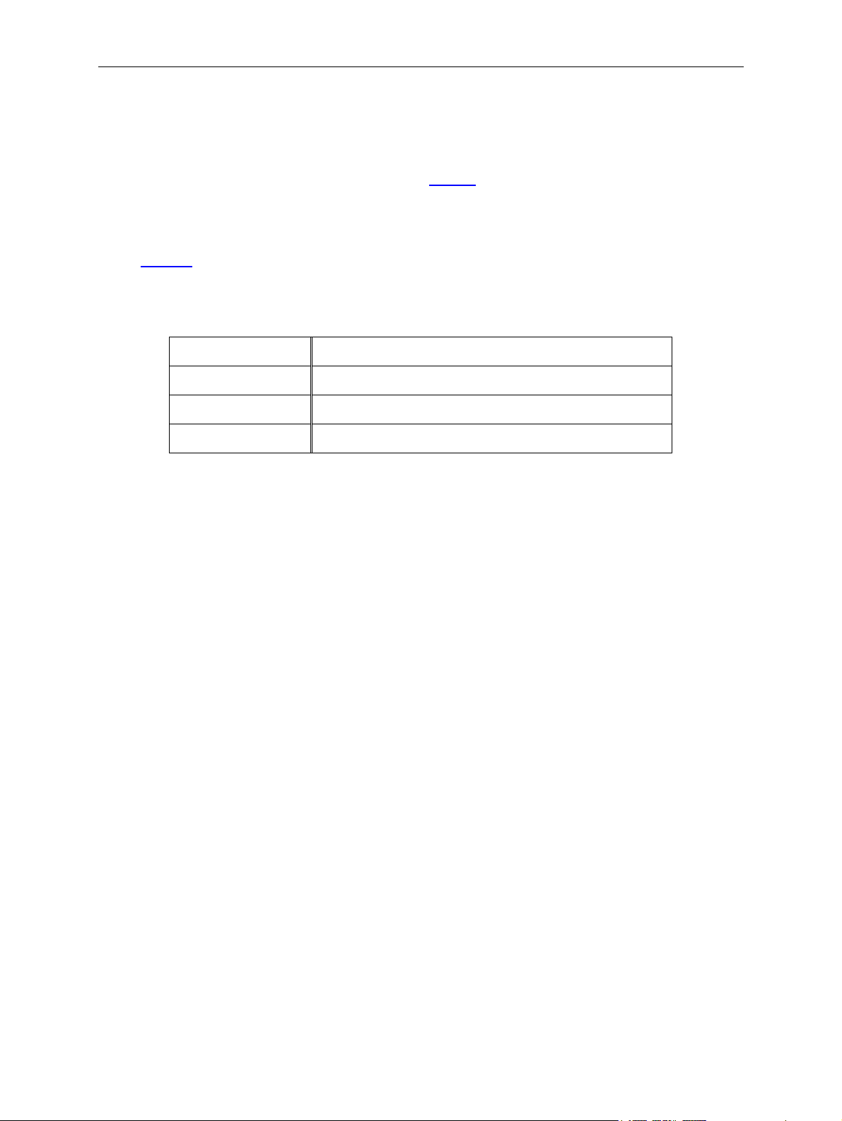
7. Debug Features
Debug features are used to determine reasons for coin reject, and are output on the coin
acceptor LED by a number of red pulses (see Table 3 below).
The coin acceptor LED under normal operation should be GREEN.
The LED is situated above the 6 way DIL switch on the connector side on the acceptor (See
Figure 6).
Table 3: Debug Features
1 RED pulse Coin accepted / reject lever pressed
2 RED pulses Coin outside programmed sensor windows
3 RED pulses Coin valid, but inhibited
4 RED pulses Master Inhibit from host machine
Debug features will not be buffered and assume a single coin insertion. The insertion of several
coins would cause an overflow and no useful information.
The debug features operate in normal acceptor operation.
The LED cannot be seen if the machine door is closed.
Money Controls 2005. All rights reserved.
Page 14 of 50
Page 15
SR3 Type 1 Technical Manual TSP005.doc Issue 5.0 – Jan 2005
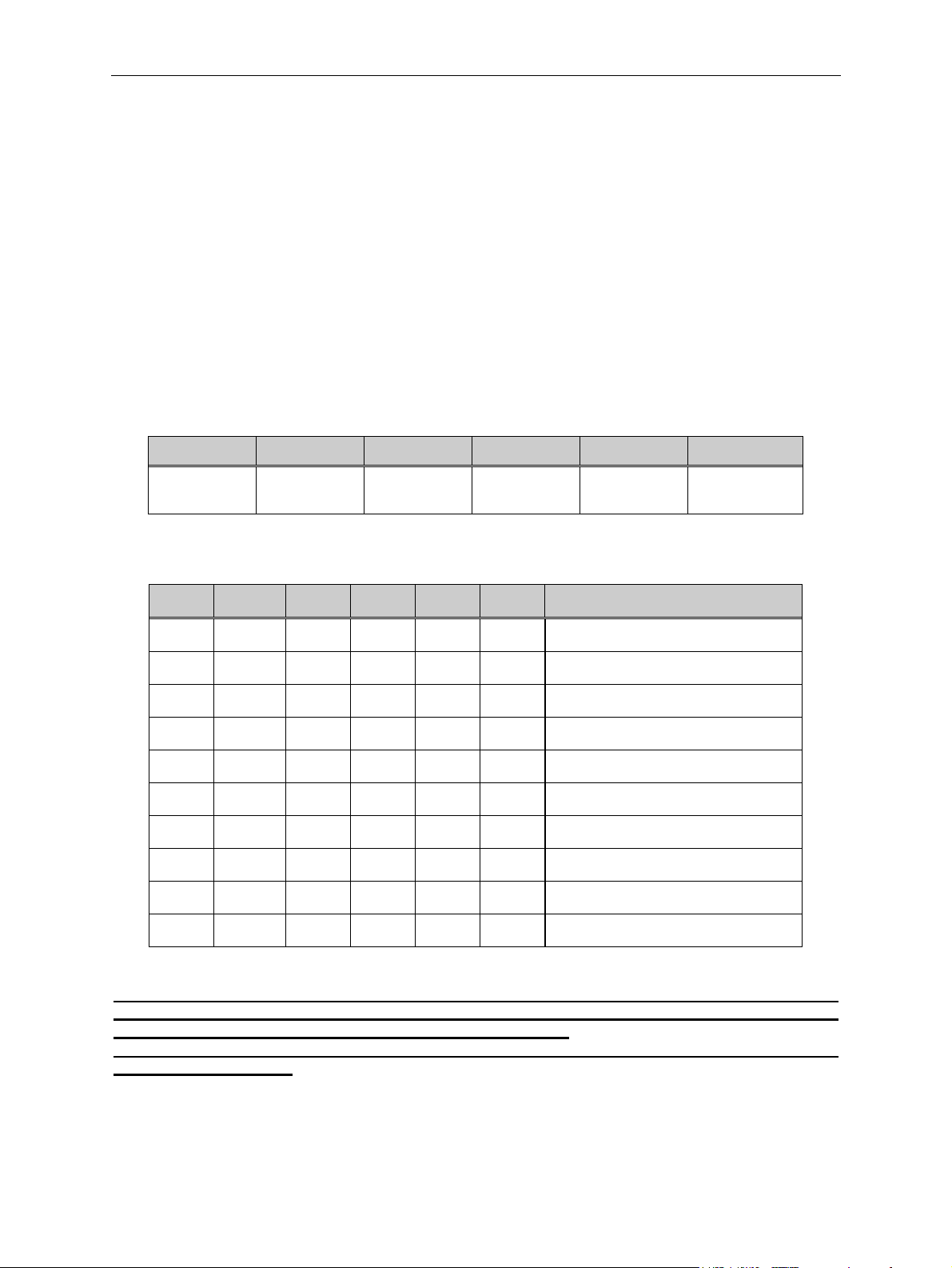
8. DIL Switch Options.
There are a number of options which can be selected via the 6 way DIL switch.
The 6 way DIL switch or Program Switch Bank can be used for field programming the following:
¾ Enable / disable a specific coin.
¾ Adjust coin security settings.
¾ Bank select.
¾ Enable / disable alarm.
¾ Teach and Run
¾ Erase all windows.
Table 4: DIL Switch Functions
1 2 3 4 5 6
TM
.
Program 1 Program 2 Program 3 Program 4 Teach on/off
Table 5: SR3 DIL Switch Guide
SW1 SW2 SW3 SW4 SW5 SW6 FUNCTION
off off off off off off *Test credit accumulator
off
ON ON
off off off
ON
off
ON
ON ON
off off
ON
ON
off off
ON
off off off off off Erase all windows ( Step 2 )
off
off off off off Enable bank 1 and bank 2
off off off off Enable a coin
ON
ON
off
off
ON ON
ON ON
ON
ON
off off Disable alarm
off off Enable alarm
off off Erase all windows ( Step 1 )
off off Inhibit a coin
off off Enable bank 1 only
off off Enable bank 2 only
Security
on/off
* NOTE:- If all the switches are OFF and the reject lever is pressed within 20 seconds of power
being applied, the SR3 will enter “Test credit accumulator” mode, even though one may not be
fitted. The LED will turn RED and no coins will be accepted.
To exit this mode either remove power and re-apply or wait a further 20 seconds and the SR3
will automatically reset.
Money Controls 2005. All rights reserved.
Page 15 of 50
Page 16
SR3 Type 1 Technical Manual TSP005.doc Issue 5.0 – Jan 2005
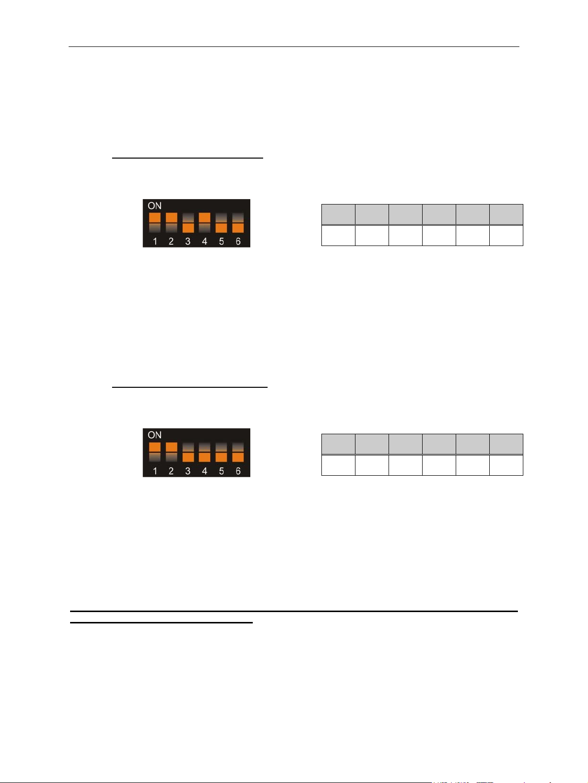
9. Accept and Inhibit Configuration
It is possible on the SR3 to inhibit a single coin or any combination of the 12 possible
programmed coins by following the procedure below.
9.1 To Inhibit Specific Coins
Example:- To Inhibit 50p and 20p.
Switch off the power to the SR3.
Set the Program DIL switches to:-
SW1 SW2 SW3 SW4 SW5 SW6
Switch on the power to the SR3.
Press the reject lever within 20 seconds.
The LED will turn RED.
Insert 50p and 20p and check that they are accepted.
Press the reject lever to return to normal operational mode.
The LED will turn GREEN.
Return ALL the DIL switches to the OFF position.
The inserted coin/s will now be rejected.
9.2 To Enable Specific Coins
Example:- To Enable 50p and 20p.
Switch off the power to the SR3.
Set the Program DIL switches to:-
Switch on the power to the SR3.
Press the reject lever within 20 seconds.
The LED will turn RED.
Insert 50p and 20p and check that they are accepted.
Press the reject lever to return to normal operational mode.
The LED will turn GREEN.
Return ALL the DIL switches to the OFF position.
The inserted coin/s will now be accepted.
ON ON
SW1 SW2 SW3 SW4 SW5 SW6
ON ON
OFF
OFF OFF OFF OFF
ON
OFF OFF
Note:- It is possible for a single coin to be enabled using the above procedure even though that particular bank has been disabled.
Money Controls 2005. All rights reserved.
Page 16 of 50
Page 17
SR3 Type 1 Technical Manual TSP005.doc Issue 5.0 – Jan 2005
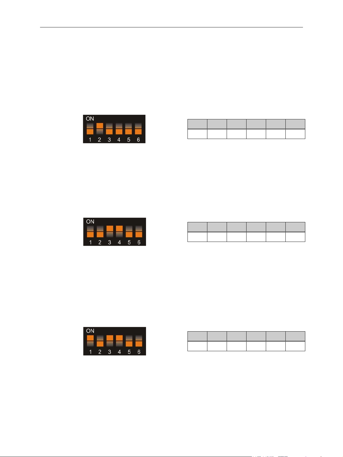
10. Bank Select
This function allows you to enable both or individually select banks of coins via the 6 way DIL
switch.
This enables the selection of 2 different currencies, one in each bank, or 12 coins/tokens in both
banks from the same country.
To enable/disable the banks follow the steps below.
10.1 Both Banks ON
Switch off the power to the SR3.
SW1 SW2 SW3 SW4 SW5 SW6
Switch on the power to the SR3.
Press the reject lever within 20 seconds.
The LED will flash GREEN.
Press the reject lever again.
The LED will be constant GREEN.
Set ALL the DIL switches to the OFF position.
Coins in Banks 1 and 2 will now be accepted.
10.2 Bank 1 ON Bank 2 OFF
Switch off the power to the SR3.
Switch on the power to the SR3.
Press the reject lever within 20 seconds.
The LED will flash GREEN.
Press the reject lever again.
The LED will be constant GREEN.
Set ALL the DIL switches to the OFF position.
Coins in bank 1 will now be accepted.
Coins in bank 2 will be rejected.
OFF
SW1 SW2 SW3 SW4 SW5 SW6
OFF OFF
ON
OFF OFF OFF OFF
ON ON
OFF OFF
10.3 Bank 1 OFF Bank 2 ON
Switch off the power to the SR3.
Switch on the power to the SR3.
Press the reject lever within 20 seconds.
The LED will flash GREEN.
Press the reject lever again.
LED will be constant GREEN.
Set ALL switches to the OFF position.
Coins in bank 1 will now be rejected.
Coins in bank 2 will be accepted.
Money Controls 2005. All rights reserved.
Page 17 of 50
SW1 SW2 SW3 SW4 SW5 SW6
ON
OFF
ON ON
OFF OFF
Page 18

SR3 Type 1 Technical Manual TSP005.doc Issue 5.0 – Jan 2005
11. Teach and Run™ Option
The SR3 can have the option to enable Teach & Run™ on all 12 coins.
This option is selected at the time of order. The specific coin channel to be programmed is
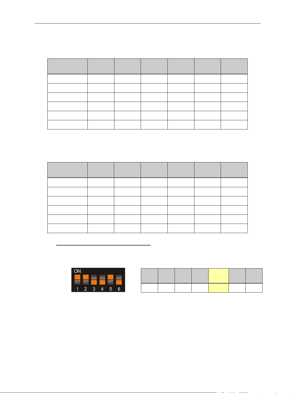
selected using switch 1 (MSB) to switch 4 (LSB) on the 6 way DIL switch.
11.1 Programming Steps
To programme a coin / token please follow these 6 Steps:
1. Switch off the power to the SR3.
2. Set the 6 way DIL switch to the relevant coin to be programmed. (See Table 6 and
Table 7 below)
3. Switch on the power to the SR3.
4. Press the reject lever.
The LED will turn RED.
5. Start entering the coins
typically after around 10 insertions
6. Press the reject lever and the LED will turn RED then GREEN.
1
or tokens1 you wish to teach until the LED flashes GREEN,
2
.
Notes:
The coin channel is now programmed
3
.
To programme further coin channels, repeat from step 1.
Once you have finished programming return all switches to the OFF position.
The first coin inserted after Teach & Run™ may reject. Subsequent coins should accept.
1
If a large sample of coins/tokens are used, then the coin channel sensor windows will
be more accurate and a higher acceptance of true coins/tokens should be seen. If only
a single coin/token is used, coin channel sensor windows will be programmed which
may not truly reflect the coin/token population.
2
If significantly more than 10 coins have been inserted and the LED is still not changing
to GREEN, this could be caused by three possible reasons.
a) The coins/tokens being used are actually 2 different types although they look
the same e.g. 1p old and 1p new.
b) The coins/tokens being used are poorly manufactured/minted to such an extent
that the Teach & Run™ is unable to correlate the readings taken.
c) The SR3 has a fault.
3
Even though a coin/token has been programmed make sure that the coin channel or
bank has actually been enabled (see sections 9 and 10
).
Teach & Run™ does NOT automatically enable the taught coin/token.
Money Controls 2005. All rights reserved.
Page 18 of 50
Page 19
SR3 Type 1 Technical Manual TSP005.doc Issue 5.0 – Jan 2005
11.2 BANK 1
Table 6: Teach and Run™ Programming - Bank 1
Coin Number Switch 1 Switch 2 Switch 3 Switch 4 Switch 5 Switch 6
1
2
3
4
5
6
Off Off Off
Off Off
Off Off
Off
Off
Off
ON
ON
ON ON
ON
ON ON ON
Off Off
Off
ON ON
Off
ON ON
Off
ON
ON
ON
11.3 BANK 2
Table 7: Teach and Run™ Programming - Bank 2
Coin Number Switch 1 Switch 2 Switch 3 Switch 4 Switch 5 Switch 6
7
8 ON
9 ON
10 ON
11 ON
Off
ON ON ON ON
Off Off Off
Off Off
Off
Off
ON
ON ON ON
ON ON
Off
ON
ON
Off
Off
Off
Off
Off
Off
Off
Off
Off
Off
Off
12 ON ON
Example:- To teach coin channel 12 for £1
Switch off the power to the SR3.
Set DIL switches to:-
Switch on the power to the SR3.
Press the reject lever within 20 seconds.
The LED will turn RED.
Start entering £1 coins into the acceptor until the LED flashes GREEN, typically after 8 to 10
insertions.
Press the reject lever and the LED will turn RED then GREEN.
The coin channel has been programmed.
Set ALL switches to the OFF position.
Money Controls 2005. All rights reserved.
Page 19 of 50
Off Off
MSB
SW1
ON ON
SW2 SW3
LSB
SW4
OFF OFF
ON
Total SW5 SW6
12 ON
Off
OFF
Page 20
SR3 Type 1 Technical Manual TSP005.doc Issue 5.0 – Jan 2005
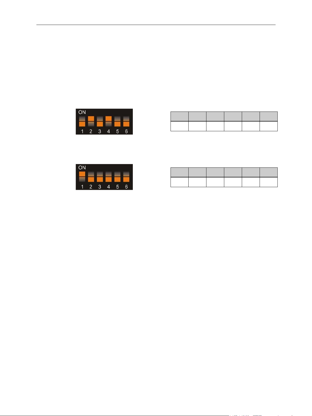
12. Erase All Windows
This function allows you to erase all the windows previously programmed, whether they were
programmed by Teach and Run
TM
, programmed using a programming device or programmed
by Money Controls Ltd.
Because of the severity of this procedure, two steps are required, which reduces the risk of this
being done accidentally.
Switch off the power to the SR3.
Set the Program DIL switches to:-
SW1 SW2 SW3 SW4 SW5 SW6
OFF
ON
OFF
ON
OFF OFF
Switch on the power to the SR3.
Press the reject lever within 20 seconds.
The LED will flash RED / GREEN.
Set the Program DIL switches to:-
SW1 SW2 SW3 SW4 SW5 SW6
ON
OFF OFF OFF OFF OFF
Press the reject lever again.
The LED will flash GREEN.
Set ALL the DIL switches to the OFF position.
Press the reject lever to return to operational mode.
LED will change to constant GREEN.
Money Controls 2005. All rights reserved.
Page 20 of 50
Page 21
SR3 Type 1 Technical Manual TSP005.doc Issue 5.0 – Jan 2005
13. Adjustable Coin Security
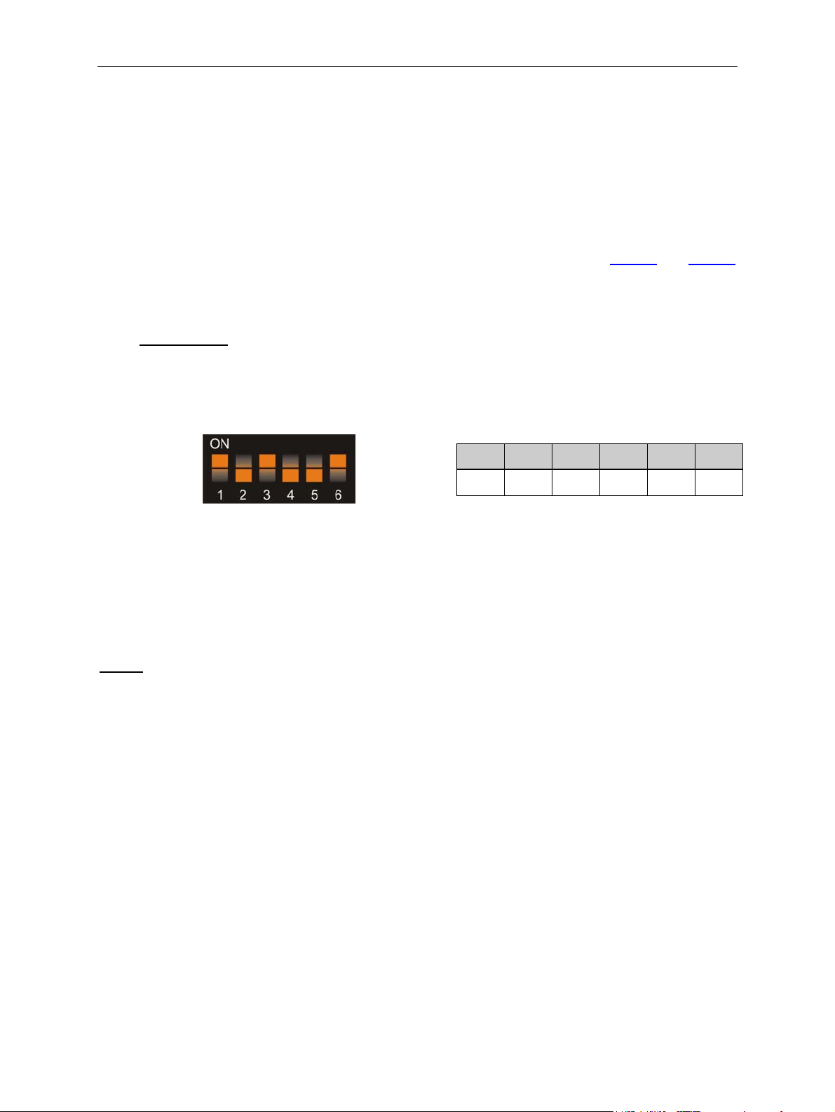
The security of an individual coin/token can be adjusted using the 6 way DIL switches.
Switch 1 Allows sensor windows to be increased or decreased. (ON = increase
windows / decrease security, OFF = decrease windows / increase
security)
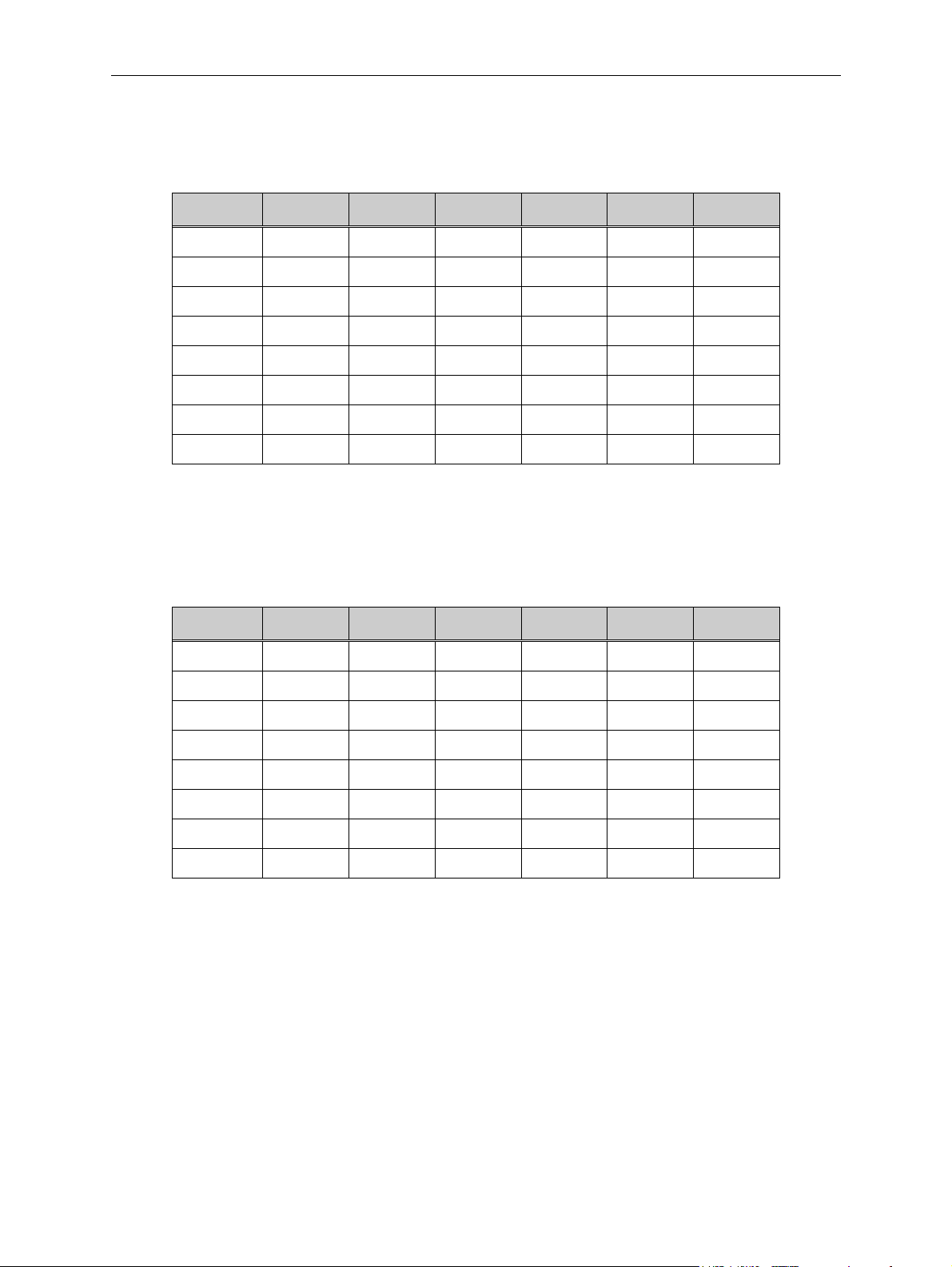
Switches 2, 3, 4 Determines the number of counts to be added or removed from the
sensor windows (SW2 = MSB, SW4 = LSB). See Table 8 and Table 9
below.
Switch 5 Not used for adjusting coin security settings = OFF.
Switch 6 Enables coin security mode = ON.
For Example:
To increase the sensor windows / decrease the security on a £1 coin4 by 2 counts
following procedure should be followed:
Switch off the power to the SR3.
Set the 6 way DIL switches to:- (widen, 2 counts, security)
SW1 SW2 SW3 SW4 SW5 SW6
ON
OFF
ON
Switch on the power to the SR3.
Press the reject lever within 20 seconds and check the LED turns RED.
Insert a £1 coin.
The LED now flashes GREEN.
Press the reject lever again.
The LED will now turn RED then GREEN.
The security has now been changed.
Set ALL the switches to the OFF position.
Notes:
4
The coin channel must be ENABLED for changes to be programmed.
5
+n counts will add n counts to the upper limits of the sensor windows and subtract n
counts from the lower limits of the sensor windows for the coin channel selected. i.e.
+2 counts will actually make the sensor windows a total of 4 counts wider on the coin
channel selected.
-n counts will subtract n counts from the upper limits of the sensor windows and add
n counts to the bottom limits of the sensor windows for the coin channel selected.
i.e. +3 counts will actually make the sensor windows a total of 6 counts narrower on
the coin channel selected.
6
If 2 counts were not enough and 3 counts were actually required, the procedure has
to be repeated for +3 counts (NOT an extra +1 count).
OFF OFF
5,6
the
ON
Money Controls 2005. All rights reserved.
Page 21 of 50
Page 22
SR3 Type 1 Technical Manual TSP005.doc Issue 5.0 – Jan 2005
13.1 Decrease Security
Table 8: DIL Switches - Decrease Security
Value SW1 SW2 SW3 SW4 SW5 SW6
0 ON
+1 ON
+2 ON
+3 ON
+4 ON ON
+5 ON ON
+6 ON ON ON
+7 ON ON ON ON
13.2 Increase Security
Table 9: DIL Switches - Increase Security
Value SW1 SW2 SW3 SW4 SW5 SW6
0
-1
Off Off Off Off Off
Off Off Off
Off Off Off Off
Off Off
Off
Off
ON
ON ON
Off Off Off
Off
ON
Off Off
ON
Off Off
ON
Off
Off
Off
Off
Off
ON
ON
ON
ON
ON
ON
ON
ON
ON
ON
-2
-3
-4
-5
-6
-7
Off Off
Off Off
Off
Off
Off
Off
13.3 Reset Security
Set the DIL switches to either Increase Security 0 or Decrease Security 0. This will set the
sensor windows tweak value to 0 for the coin channel selected, i.e. the original programmed
sensor windows.
ON
ON ON
ON
ON
ON ON
ON ON ON
Off Off Off
Off
Off Off
ON
Off Off
Off
Off
Off
ON
ON
ON
ON
ON
ON
Money Controls 2005. All rights reserved.
Page 22 of 50
Page 23
SR3 Type 1 Technical Manual TSP005.doc Issue 5.0 – Jan 2005
14. Alarms
When enabled, an alarm condition will activate all the outputs (A1 to A6) for 100ms, except for
condition iii.
Conditions which will indicate an alarm condition include:
i. An event which occurs out of sequence.
ii. A sequence of events occur which indicate a ‘Coin-on-string’ fraud is being attempted.
There are a number of events that might lead to this condition.
iii. If the credit / reject sensor is blocked for more than 1.5 seconds, the alarm signal will
remain active, for the duration of the blockage.
iv. During power-up diagnostics – if enabled.
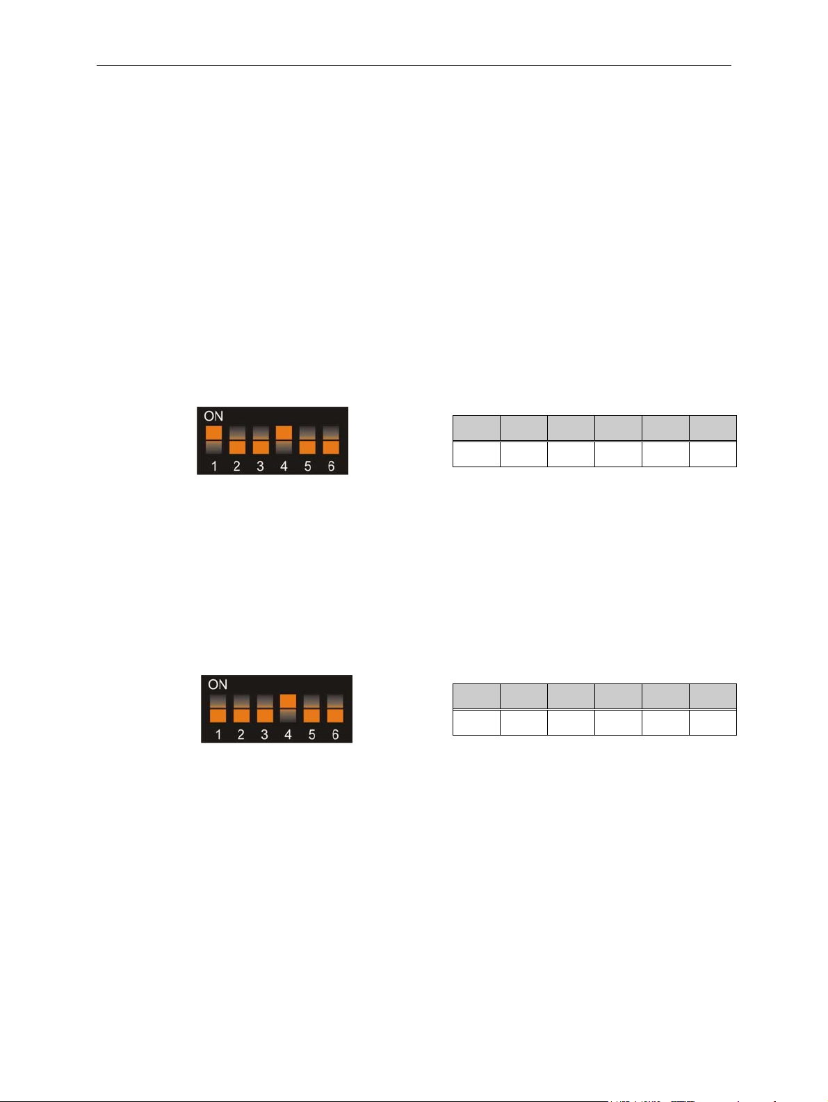
14.1 Enable
To enable an alarm the following steps should be followed:
Switch off the power to the SR3.
SW1 SW2 SW3 SW4 SW5 SW6
Switch on the power to the SR3.
Press the reject lever within 20 seconds.
The LED will flash GREEN.
Switch off the power to the SR3.
Set all switches OFF.
Switch on the power to the SR3.
The alarm is now ON.
14.2 Disable
To disable an alarm the following steps should be followed:
Switch off the power to the SR3.
Switch on the power to the SR3.
Press the reject lever within 20 seconds.
The LED will flash GREEN.
Switch off the power to the SR3.
Set all switches OFF.
Switch on the power to the SR3.
The alarm is now OFF.
ON
SW1 SW2 SW3 SW4 SW5 SW6
OFF OFF OFF
OFF OFF
ON
ON
OFF OFF
OFF OFF
Money Controls 2005. All rights reserved.
Page 23 of 50
Page 24

SR3 Type 1 Technical Manual TSP005.doc Issue 5.0 – Jan 2005
15. Diagnostics (power-up)
The SR3 performs a self-test at power-up. If a fault condition is detected and diagnostics is
enabled, an Alarm is activated and the SR3 is inhibited. If the fault condition clears, say a coin
blockage of the credit sensor, the inhibit will be lifted and the SR3 is then ready for normal
operation. A diagnostics test failure is indicated in parallel mode in exactly the same way as an
alarm.
The faults which are detected at power up are:-
¾ Credit sensor blocked.
¾ EEPROM checksum error.
¾ Blockage in the discrimination area.
¾ Sensor faulty.
16. Sorter Option
The SR3 can drive an external 5/6-way sorter. The SR3 and sorter attach to a new style
frontplate. The coin exit positions from the sorter are identical to an industry standard OEM
product. There are two operating modes for use with sorters. One mode is selected during the
setup process.
16.1 Sorter Mode 1 (default)
The SR3 provides a logic signal to enable the sorter solenoids to be driven. The signal is
active for 500ms and generated at the same time as the accept gate is activated There is no
feedback from the sorter.
16.2 Sorter Mode 2
As soon as a coin is discriminated as true, its corresponding credit code is output for 1ms,
after which the accept gate and sorter solenoids are activated. [provided Inhibit All is
inactive].
If the Inhibit All is active (i.e. all coins inhibited), then the credit code is output for 10ms. No
accept gate solenoid activity occurs and the coin is rejected. If during the first 9ms of the
10ms credit pulse, the Inhibit All changes to inactive (i.e. accept), then the coin will be
accepted. The accept gate then operates and the coin accepts. A 100ms credit is issued as
the coin passes the credit sensor.
The host machine drives the sorter solenoids in this application.
16.3 Sorter Mode 3
The issue of the ‘early’ 1ms credit is delayed by a fixed time from completion of coin
discrimination (TBD). Provided the Inhibit All line is inactive when the coin completes
discrimination, the coin accepts. The early credit pulse is issued after the fixed delay,
followed by the standard credit pulse of 100ms duration as the coin passes the credit sensor.
Note: Sorter modes 1, 2 & 3 are mutually exclusive. One must be selected when ordering.
Money Controls 2005. All rights reserved.
Page 24 of 50
Page 25
SR3 Type 1 Technical Manual TSP005.doc Issue 5.0 – Jan 2005
17. Sorter Drivers
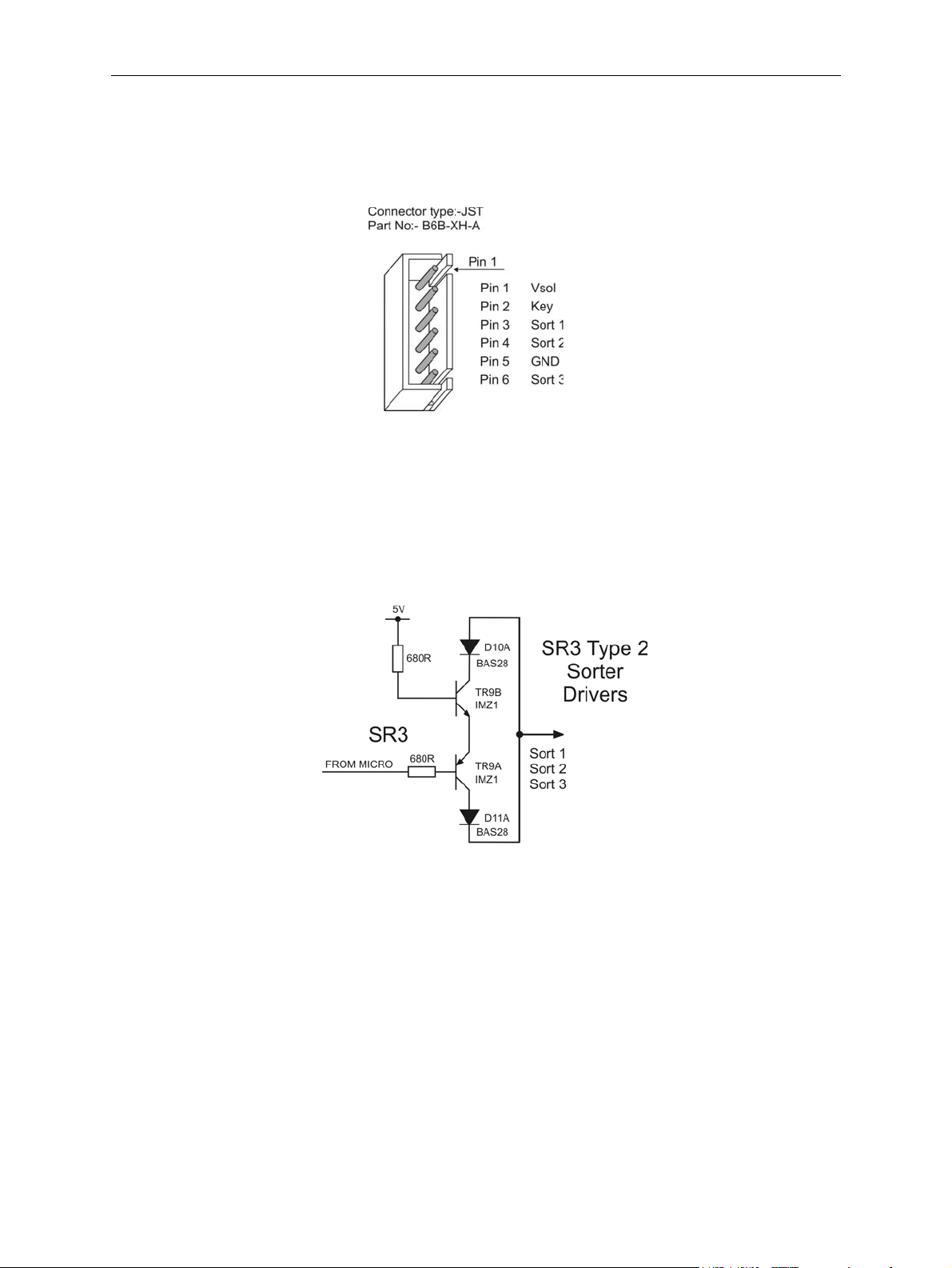
Figure 10: Sort Output Connector Details
17.1 Sorter Drive Circuit
The sorter output on SR3 is just a low current drive and will not drive a solenoid directly. It
was designed to source or sink a limited current and so it can be connected directly to the
base of the transistor being used to drive the solenoid.
Figure 11: Sorter Drive Output Circuit
17.11 THEORY OF OPERATION
If SORT 1 / 2 / 3 is connected to +5V or above, D11A is reverse biased and D10A
forward biased. To turn on the drive, the micro takes it's output to 0V, enabling TR9B to
sink current which flows through R83 until the voltage on the base of TR9A reaches
about 3.8V. At this point the voltage on the base of TR9B will be approaching 5V so it will
start to turn off. The current sink is therefore limited to about 5mA (as the micro output is
at around 0.4V, the current through R83 is (3.8-0.4)/680). If SORT 1 / 2 / 3 is connected
to 0V or below, D10A is reverse biased and D11A forward biased. The circuit works in a
similar way and TR9B sources current until the voltage across R82 has dropped to nearly
1.2V, so again the output current source is limited to 5mA.
Money Controls 2005. All rights reserved.
Page 25 of 50
Page 26
SR3 Type 1 Technical Manual TSP005.doc Issue 5.0 – Jan 2005
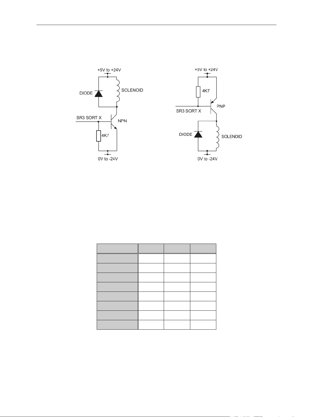
17.2 Sorter Drive Examples
Figure 12: Sorter Drive Examples
These two circuits show how you could use the SR3 output to drive a solenoid. The
transistors used depend on how much current your solenoid requires. The above voltages
show the maximum range you can apply to the SR3 output and you will need to set the
actual voltage to match your solenoid.
17.3 Sort Outputs v Sorter Paths
Table 10: Sort Outputs v Sorter Paths
Sorter Path Sort 1 Sort 2 Sort 3
1
2
3
4
5
6
7
8
100
010
000
110
101
011
001
111
1 = Active
Money Controls 2005. All rights reserved.
Page 26 of 50
Page 27

SR3 Type 1 Technical Manual TSP005.doc Issue 5.0 – Jan 2005
18. Totaliser Mode
By connecting an additional ‘piggy back’ PCB to the SR3, (Figure 1 Connector 5), totalising
functions are available. It is advisable to have the SR3 set-up in this mode if it is at all possible
that the totaliser function may be used.
If a totaliser PCB is not connected, the SR3 will function normally.
NOTE: If the totaliser is fitted, credits can be obtained from the totaliser output AND the standard SR3 10 way interface simultaneously.
The totaliser board provides the following physical interface to the machine.
18.1 19 way Parallel Interface Connector
Table 11: 19 way Parallel Interface Connector
Pin No. Function I/P - O/P
1
2
3
4
5
6
7
8
9
10
11
12
13
14
15
16
No Function
No Function
No Function
No Function
CMETER (Coin Meter) O/P
No Function
No Function
V Supply 12V
Player 1 HI O/P
Player 1 LOW O/P
No Pin
GND
Dispense 1 I/P
Player 2 O/P
Dispense 2 I/P
Player 3 O/P
17
18
19
This connector provides all the control pins for totalising for up to 4 players including supply
voltages.
Dispense 3 I/P
Player 4 O/P
Dispense 4 I/P
Money Controls 2005. All rights reserved.
Page 27 of 50
Page 28
SR3 Type 1 Technical Manual TSP005.doc Issue 5.0 – Jan 2005
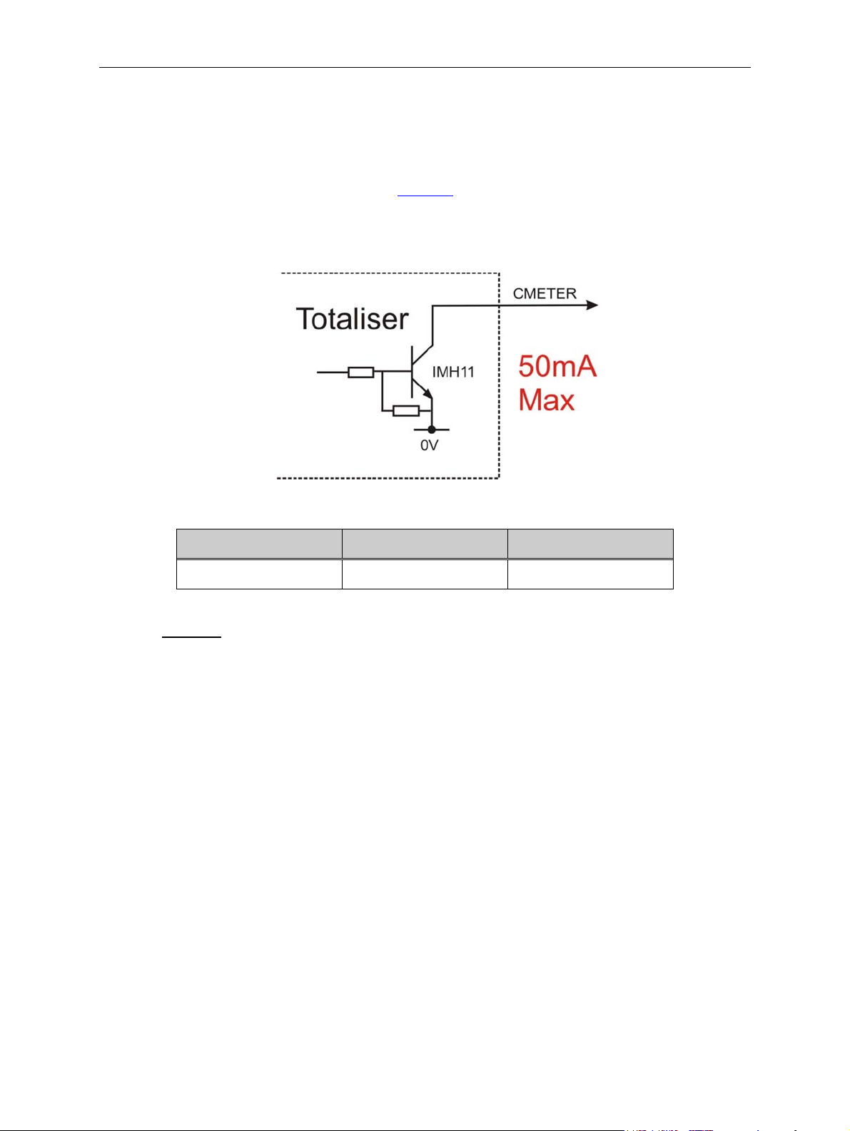
18.2 CMETER
CMETER (coin meter) sends out a number of active low pulses every time a coin is
discriminated and accepted, the number of pulses and their time width is pre-programmed at
MCL, or using a ccProgrammer. See Table 13
Figure 13: CMETER Output
OFF State Voltage ON State Voltage Sink Current
+30V DC Max +0.5 V DC Max 50mA Max
Example:
If a coin is accepted by the SR3, which has a credit value of 80 and the Coin Meter Scalar
value is 20 then 4 pulses are output by the CMETER pin.
Money Controls 2005. All rights reserved.
Page 28 of 50
Page 29
SR3 Type 1 Technical Manual TSP005.doc Issue 5.0 – Jan 2005
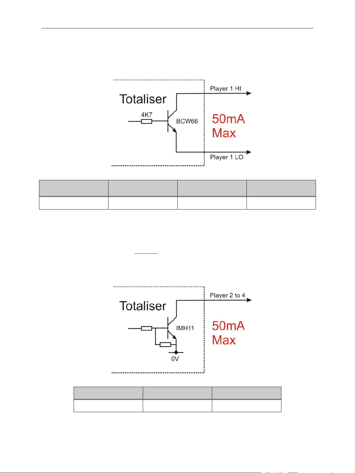
18.3 Player 1 HI / Player 1 LO
Figure 14: Player 1 HI / Player 1 LO Output
OFF State Voltage
(Player 1 HI)
+30V DC Max +0.5 V DC Max 0V Min 50mA Max
ON State Voltage
(Player 1 HI)
ON State Voltage
(Player 1 LO)
Sink Current
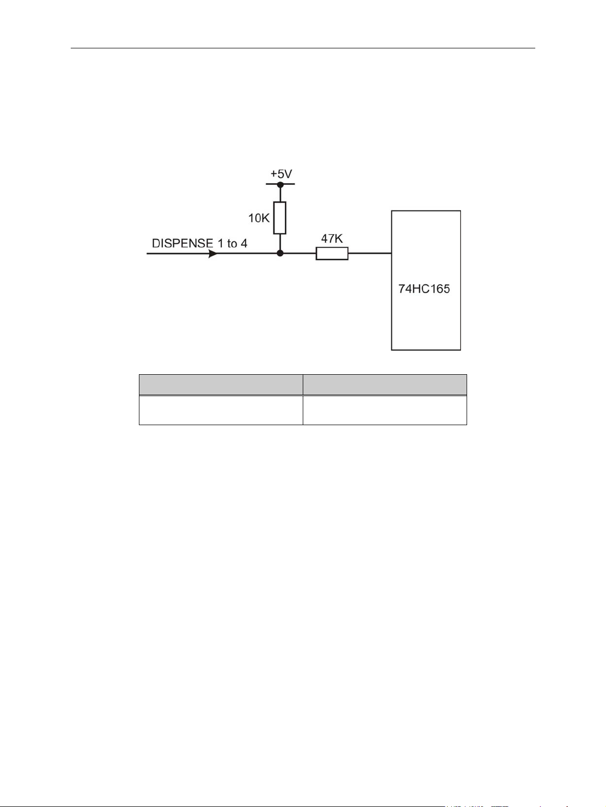
18.4 Player 2 to 4
Indicates a game output to the relevant player. Game pulse width is defined by
the parameters shown in Table 13.
Figure 15: Player 2 to 4 Outputs
OFF State Voltage ON State Voltage Sink Current
+30V DC Max +0.5 V DC Max 50mA Max
Money Controls 2005. All rights reserved.
Page 29 of 50
Page 30
SR3 Type 1 Technical Manual TSP005.doc Issue 5.0 – Jan 2005
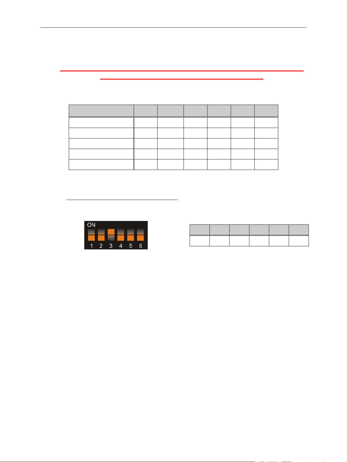
18.5 Dispense 1 to 4
Indication from the host machine that it is ready for a Game pulse from the corresponding
PLAYER 1 to 4 output.
Figure 16: Dispense 1 to 4 Inputs
Inactive Vin Active Vin
> +4V DC (+30V DC Max) Between 0V and +1V DC
Money Controls 2005. All rights reserved.
Page 30 of 50
Page 31
SR3 Type 1 Technical Manual TSP005.doc Issue 5.0 – Jan 2005
19. Totalising Options
The following information ONLY applies to a SR3 type 1 (piggy back style
totaliser) and NOT a SR3 type 2 (totaliser in-built)
Table 12: SR3 Totalising DIL Switch Guide
FUNCTION
Set Game Price off off
Set Bonus Level 1 off
Set Bonus Level 2 off
Set Bonus Award 1
Set Bonus Award 2
19.1 Set a Game Price
Example:- To set the price of 1 game at £1
Switch off the power to the SR3.
Set the Program DIL switches to:-
Switch on the power to the SR3.
Press the reject lever within 20 seconds.
The LED will turn RED.
Insert any combination of programmed coins that total £1 and check that they are accepted,
i.e. 1 x £1, 2 x 50p, 5 x 10p + 1 x 50p etc.
Press the reject lever to return to normal operational mode.
The LED will turn GREEN.
Return ALL the DIL switches to the OFF position.
SW1 SW2 SW3 SW4 SW5 SW6
ON
ON ON
ON ON ON
ON ON ON
ON ON ON ON
SW1 SW2 SW3 SW4 SW5 SW6
OFF OFF
off off off
off off off
off off
off off off
off off
ON
OFF OFF OFF
Money Controls 2005. All rights reserved.
Page 31 of 50
Page 32
SR3 Type 1 Technical Manual TSP005.doc Issue 5.0 – Jan 2005
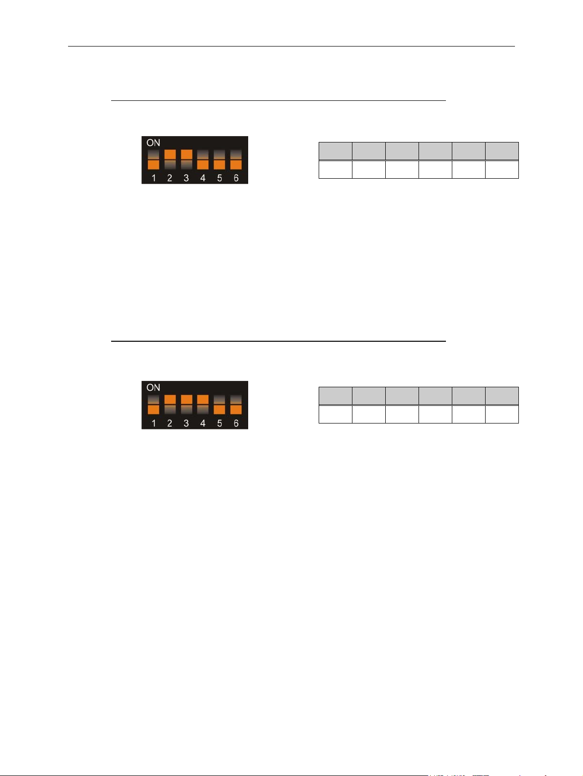
19.2 Set Bonus Level 1
Example:- When the game price is £1 and a bonus level is required at £2.50.
Switch off the power to the SR3.
Set the Program DIL switches to:-
SW1 SW2 SW3 SW4 SW5 SW6
Switch on the power to the SR3.
Press the reject lever within 20 seconds.
The LED will turn RED.
Insert any combination of programmed coins that total £2.50 and check that they are
accepted, i.e. 2 x £1 + 1 x 50p, 5 x 50p etc.
Press the reject lever to return to normal operational mode.
The LED will turn GREEN.
Return ALL the DIL switches to the OFF position.
19.3 Set Bonus Level 2
Example:- When the game price is £1 and bonus level 2 is required at £5.00.
Switch off the power to the SR3.
Set the Program DIL switches to:-
Switch on the power to the SR3.
Press the reject lever within 20 seconds.
The LED will turn RED.
Insert any combination of programmed coins that total £5.00 and check that they are
accepted, i.e. 5 x £1, 10 x 50p etc.
Press the reject lever to return to normal operational mode.
The LED will turn GREEN.
Return ALL the DIL switches to the OFF position.
OFF
SW1 SW2 SW3 SW4 SW5 SW6
OFF
ON ON
ON ON ON
OFF OFF OFF
OFF OFF
Money Controls 2005. All rights reserved.
Page 32 of 50
Page 33
SR3 Type 1 Technical Manual TSP005.doc Issue 5.0 – Jan 2005
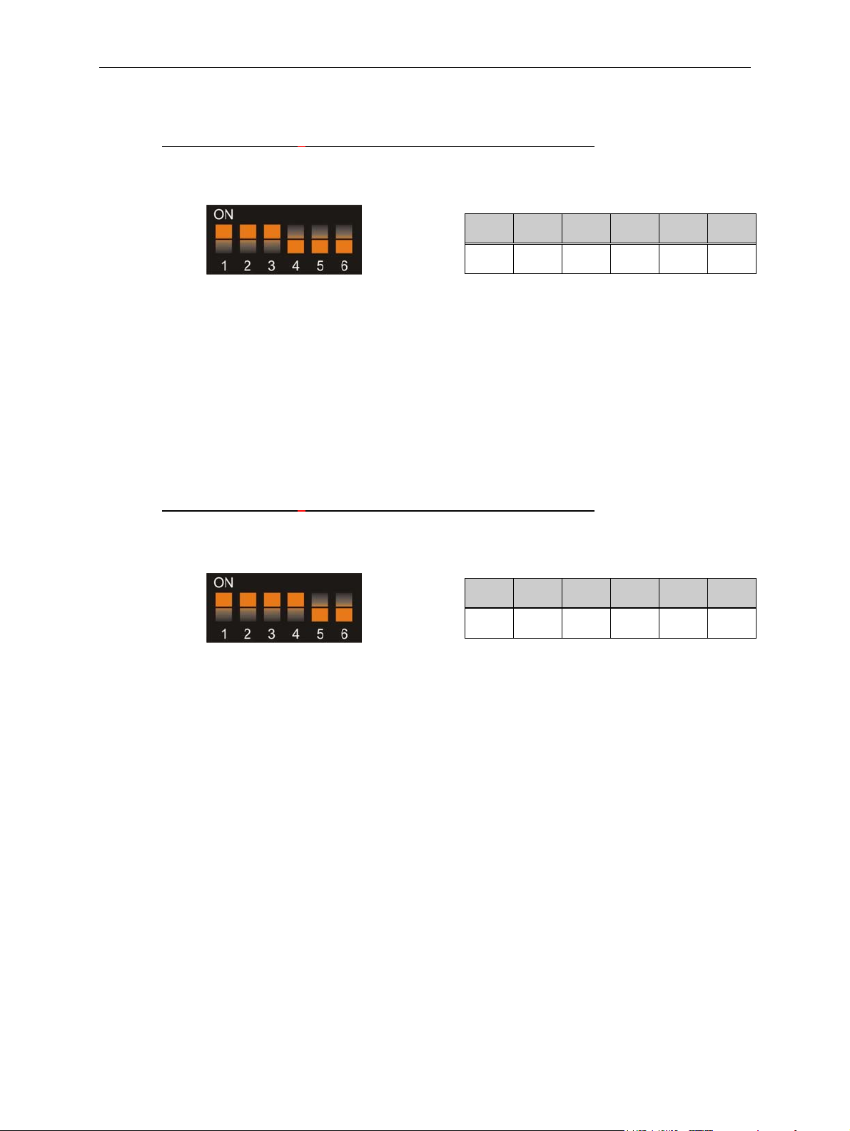
19.4 Set Bonus Award Level 1
Example:- To award 3 extra games when Bonus Level 1 is reached.
Switch off the power to the SR3.
Set the Program DIL switches to:-
SW1 SW2 SW3 SW4 SW5 SW6
Switch on the power to the SR3.
Press the reject lever within 20 seconds.
The LED will turn RED.
Insert THREE of the programmed coins and check that they are accepted, i.e. 3 x £1, 1 x
50p + 1 x 10p + 1 x 20p etc.
Press the reject lever to return to normal operational mode.
The LED will turn GREEN.
Return ALL the DIL switches to the OFF position.
19.5 Set Bonus Award Level 2
Example:- To award 7 extra games when Bonus Level 2 is reached.
Switch off the power to the SR3.
Set the Program DIL switches to:-
Switch on the power to the SR3.
Press the reject lever within 20 seconds.
The LED will turn RED.
Insert SEVEN of the programmed coins and check that they are accepted, i.e. 7 x £1, 3 x
50p + 4 x 20p etc.
Press the reject lever to return to normal operational mode.
The LED will turn GREEN.
Return ALL the DIL switches to the OFF position.
ON ON ON
SW1 SW2 SW3 SW4 SW5 SW6
ON ON ON ON
OFF OFF OFF
OFF OFF
Money Controls 2005. All rights reserved.
Page 33 of 50
Page 34
SR3 Type 1 Technical Manual TSP005.doc Issue 5.0 – Jan 2005
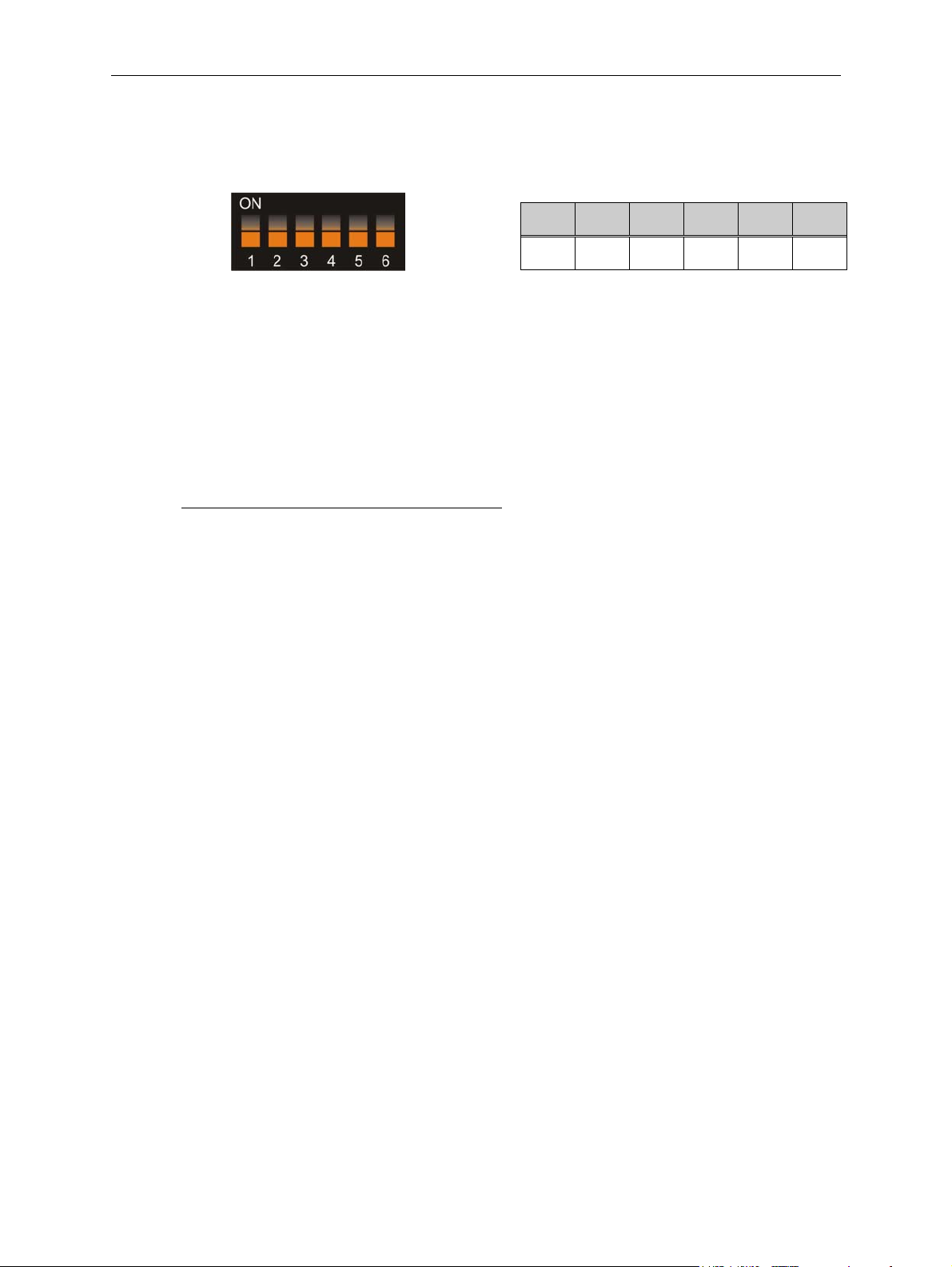
19.6 Test Credit Mode
Switch off the power to the SR3.
Set the Program DIL switches to:-
SW1 SW2 SW3 SW4 SW5 SW6
OFF OFF OFF OFF OFF OFF
Switch on the power to the SR3.
Press the reject lever within 20 seconds.
The LED will turn RED.
If manual
1
credit dispense mode is enabled then the SR3 will accumulate the test credits
each time the reject lever is pressed. If a Dispense input then goes low – BEFORE timeout
occurs – then these credits will be output on the corresponding Player output. If timeout
occurs before a Dispense input changes, the credits will be lost.
If in automatic
2
credit dispense mode then the test credits will be issued to the host machine
each time the reject lever is pressed.
Example: In Automatic credit dispense mode.
Press the reject lever 5 times, 5 game pulses will be output on the PLAYER 1 pin.
Wait 20 seconds for the SR3 to return to normal operational mode.
The LED will turn GREEN.
1
Manual credit dispense mode is available in either ‘single player mode’ or ‘multi-player
mode’ and is programmed by MCL or using a ccProgrammer.
2
Automatic credit dispense mode is only available in ‘single-player mode’ and is
programmed by MCL or using a ccProgrammer.
Money Controls 2005. All rights reserved.
Page 34 of 50
Page 35

SR3 Type 1 Technical Manual TSP005.doc Issue 5.0 – Jan 2005
19.7 Summary of Totalising Functions
With every coin that is accepted by the SR3, the accumulated credit value is incremented by
the value of that coin.
The SR3 can be used for either single (PLAYER1) or multi-player (PLAYER1-4) operation.
The SR3 can be configured at MCL or using a ccProgrammer, for either automatic or manual
credit dispense.
If the Mech. is used for single player operation then either automatic or manual credit
dispense can be pre-programmed.
If the Mech. is used for multi-player operation then manual credit dispense mode MUST be
pre-programmed at MCL or using a ccProgrammer.
In manual credit dispense mode
Game pulses are sent to a PLAYER output when the corresponding DISPENSE input
goes low and the accumulated credit exceeds the game price. After each game pulse the
accumulated credit value decrements by the value of the game price, and any remaining
credit is stored for later use.
For Example:
When DISPENSE 3 input pin goes low, (request from the host machine), and the
accumulated credit exceeds the game price, then the PLAYER3 output transistor (active
low) will switch on for the required pulse time as defined in Table 13.
In automatic credit dispense mode (Single player only)
Game pulses are output on the PLAYER 1 pin every time the accumulated credit exceeds
the game price.
A maximum number of games is pre-programmed at MCL or using a ccProgrammer, when
reached, prevents further coin acceptance.
Two bonus credit level settings can be defined and at each level a pre-specified number of
bonus games are given. The additional games are given provided the bonus credit level is
reached within a programmable time period. Refer to Bonus Levels modes 1 and 2, (Pages 32
and 33), and Bonus Awards modes 1 and 2, (Page 33) and Table 13.
Money Controls 2005. All rights reserved.
Page 35 of 50
Page 36

SR3 Type 1 Technical Manual TSP005.doc Issue 5.0 – Jan 2005
20. Totalising Parameters
The following list of parameters are pre-programmed at MCL or using a ccProgrammer.
Further explanation of parameters:
Bonus Time Width:
Time out period after last coin entered while bonus is still valid.
Example: A bonus game is awarded at £1.00, and 80p has been entered. You must enter
another 20p or more before the Bonus Time Width period elapses in order to be awarded the
extra game.
Credit:
Credit attributed to coin 1 = Value of Coin 1 * Payment Scalar Factor
Table 13: Totalising Parameters
Parameter Range Meaning
Price 0-65,535 Required credit for game output
Value of coin 1 - 12 0- 65,565 Real coin value divided by payment scaling factor
Bonus level 1 0-65,565 Credit trigger level 1
Bonus award 1 0-127 No. Games awarded at trigger level 1
Bonus level 2 0-65,565 Credit trigger level 2
Bonus award 2 0-127 No. Games awarded at trigger level 2
Maximum game limit 0-127 Maximum no. of games limit
Coin meter value scalar 0-255 No. of pulses = credit/coin meter scalar
Bonus credit mode 0-1 0= disable 1=enable
Coin meter output enable 0-1 0= disable 1=enable
Manual credit mode 0-1 0= disable (Automatic) 1=enable (Manual)
0= 75ms ON 75 ms OFF
1= 75ms ON 200ms OFF
Game pulse width 0-5
Coin meter pulse width 0-3
2= 100ms ON 200ms OFF
3= 100ms ON 330ms OFF
4= 150ms ON 330ms OFF
5= 330ms ON 330ms OFF
0= 50ms ON 50 ms OFF
1= 100ms ON 100ms OFF
2= 150ms ON 150ms OFF
3= 200ms ON 200ms OFF
Bonus time width 0-15 Time in steps of 2.5secs
Totaliser mode 0 - 1 0 = disable 1 = enable
Default values = 0 (factory set if totaliser option not selected)
Money Controls 2005. All rights reserved.
Page 36 of 50
Page 37
SR3 Type 1 Technical Manual TSP005.doc Issue 5.0 – Jan 2005
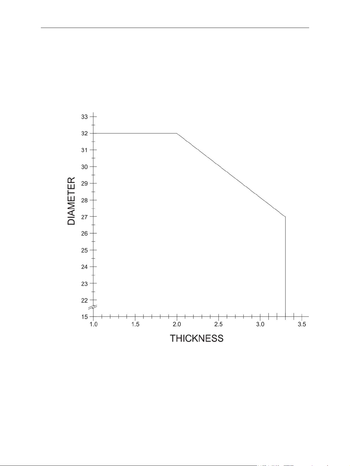
21. Coin Dimensions
The accepted range of coin sizes are shown below:
This Graph is only intended as a guide. If a coin is required that is close to the limits shown,
please check with Money Controls Technical Services department first.
Figure 17: SR3 Accepted Coin Dimensions Graph
Money Controls 2005. All rights reserved.
Page 37 of 50
Page 38
SR3 Type 1 Technical Manual TSP005.doc Issue 5.0 – Jan 2005
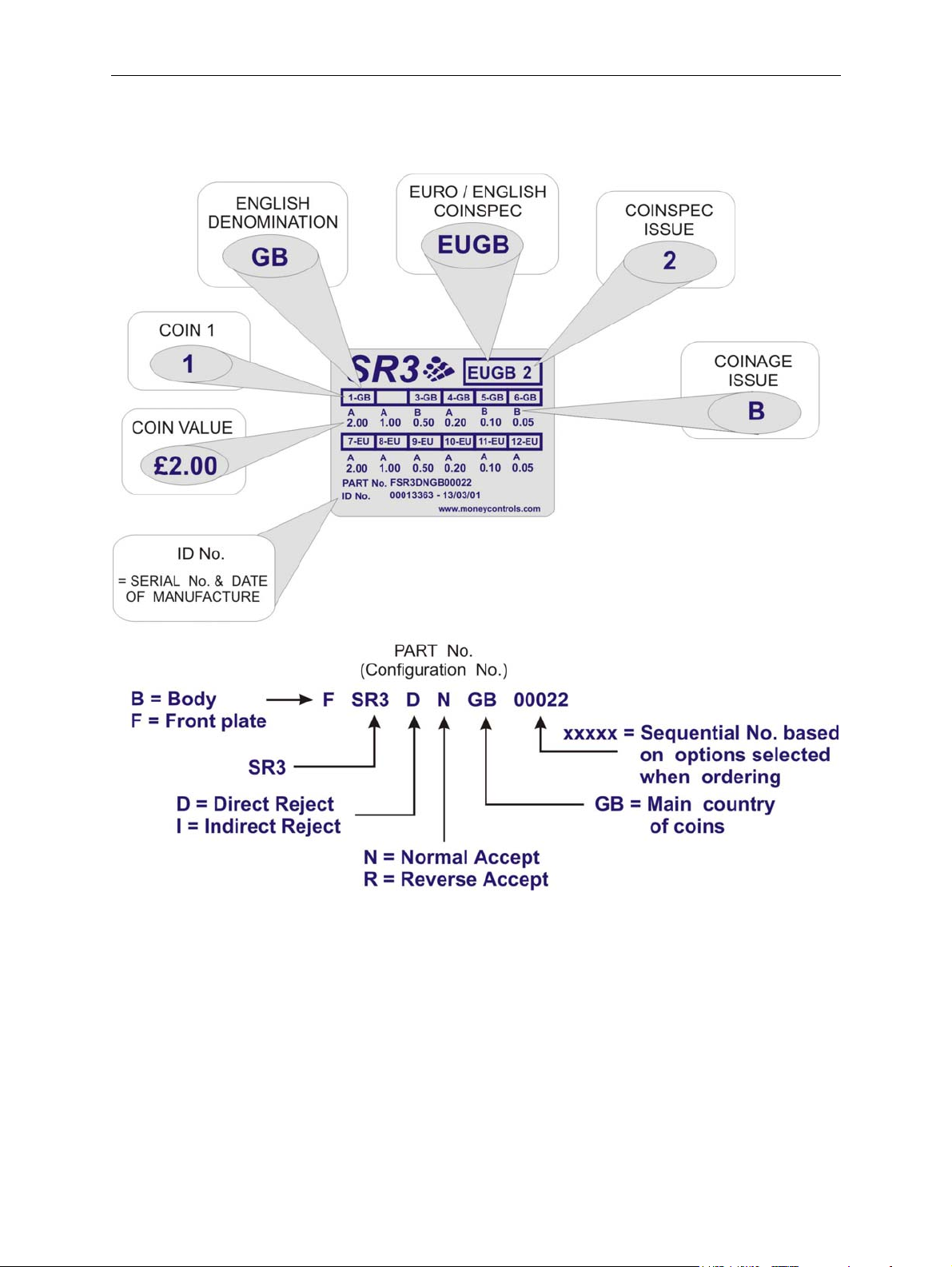
22. Label Details Explained
Money Controls 2005. All rights reserved.
Page 38 of 50
Page 39
SR3 Type 1 Technical Manual TSP005.doc Issue 5.0 – Jan 2005
23. Protocols
23.1 Serial Interface
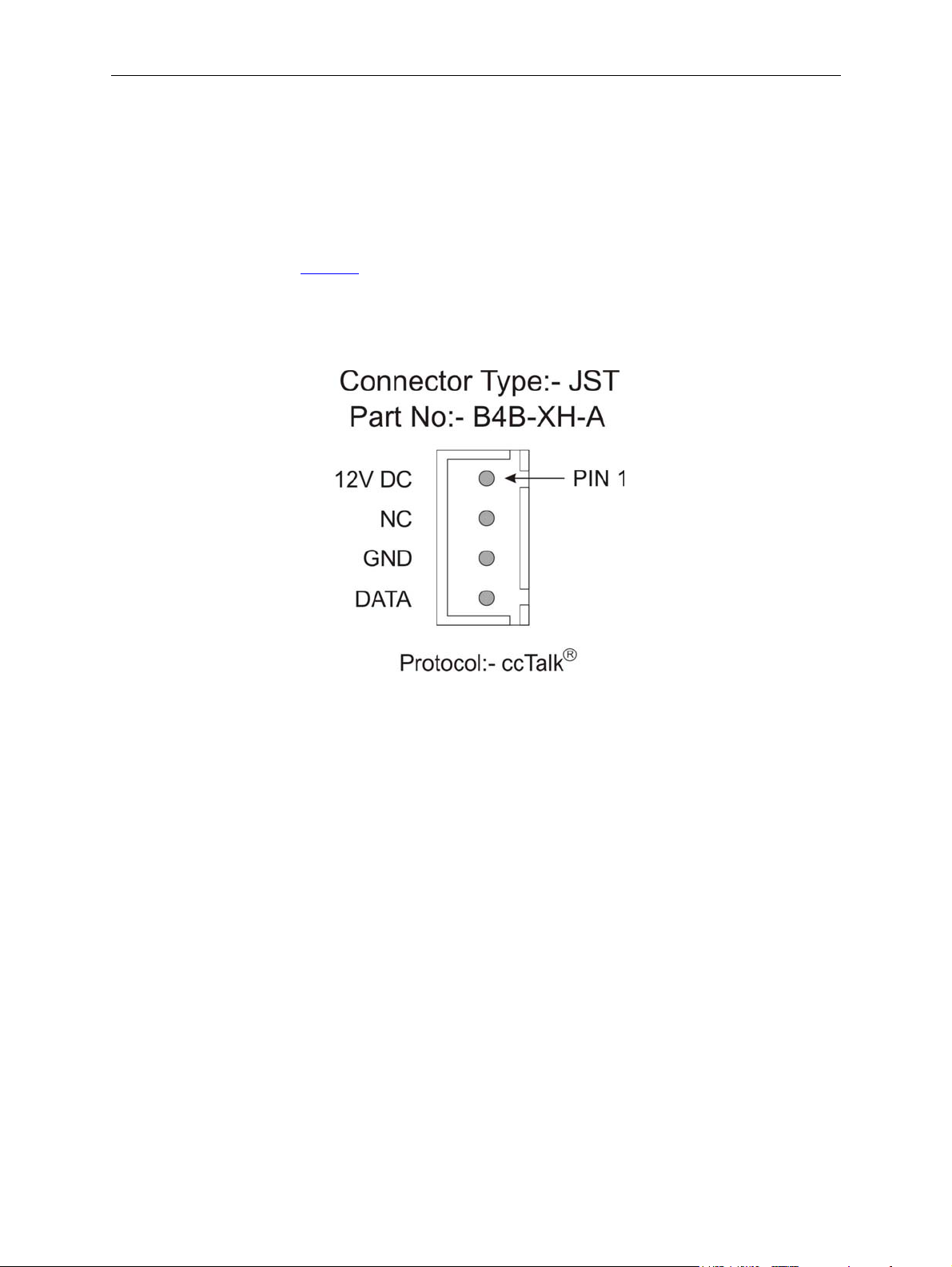
Protocol: ccTalk compliant implementation. For further details on this section please refer to
the current ccTalk generic standard.
(Connector 3 on Figure 1).
Figure 18: ccTalk Serial Connector
Money Controls 2005. All rights reserved.
Page 39 of 50
Page 40

SR3 Type 1 Technical Manual TSP005.doc Issue 5.0 – Jan 2005
24. ccTalk Serial Messages
Table 14: ccTalk Serial Commands
Header Function Header Function
254
253
252
251
250
249
248
247
246
245
244
243
242
241
240
238
Simple poll
Address poll
Address clash
Address change
Address random
Request polling priority
Request status
Request variable set
Request manufacturer id
Request equipment category id
Request product code
Request database version
Request serial number
Request software revision
Test solenoids
Test output lines
222
221
220
213
212
210
209
202
201
197
196
195
194
193
192
185
Modify sorter override status
Request sorter override status
One-shot credit
Request option flags
Request coin position
Modify sorter paths
Request sorter paths
Teach mode control
Request teach status
Calculate ROM checksum
Request creation date
Request last modification date
Request reject counter
Request fraud counter
Request build code
Modify coin id
237
236
233
232
231
230
229
227
226
225
For further details on this section please refer to the current ccTalk generic standard or contact
Money Controls Technical Services Department.
Read input lines
Read opto states
Latch output lines
Perform self-test
Modify inhibit status
Request inhibit status
Read buffered credit or error codes
Request master inhibit status
Request insertion counter
Request accept counter
Money Controls 2005. All rights reserved.
Page 40 of 50
184
183
182
173
170
169
4
3
2
1
Request coin id
Upload window data
Download calibration information
Request thermistor reading
Request base year
Request address mode
Request comms revision
Clear comms status variables
Request comms status variables
Reset device
Page 41
SR3 Type 1 Technical Manual TSP005.doc Issue 5.0 – Jan 2005
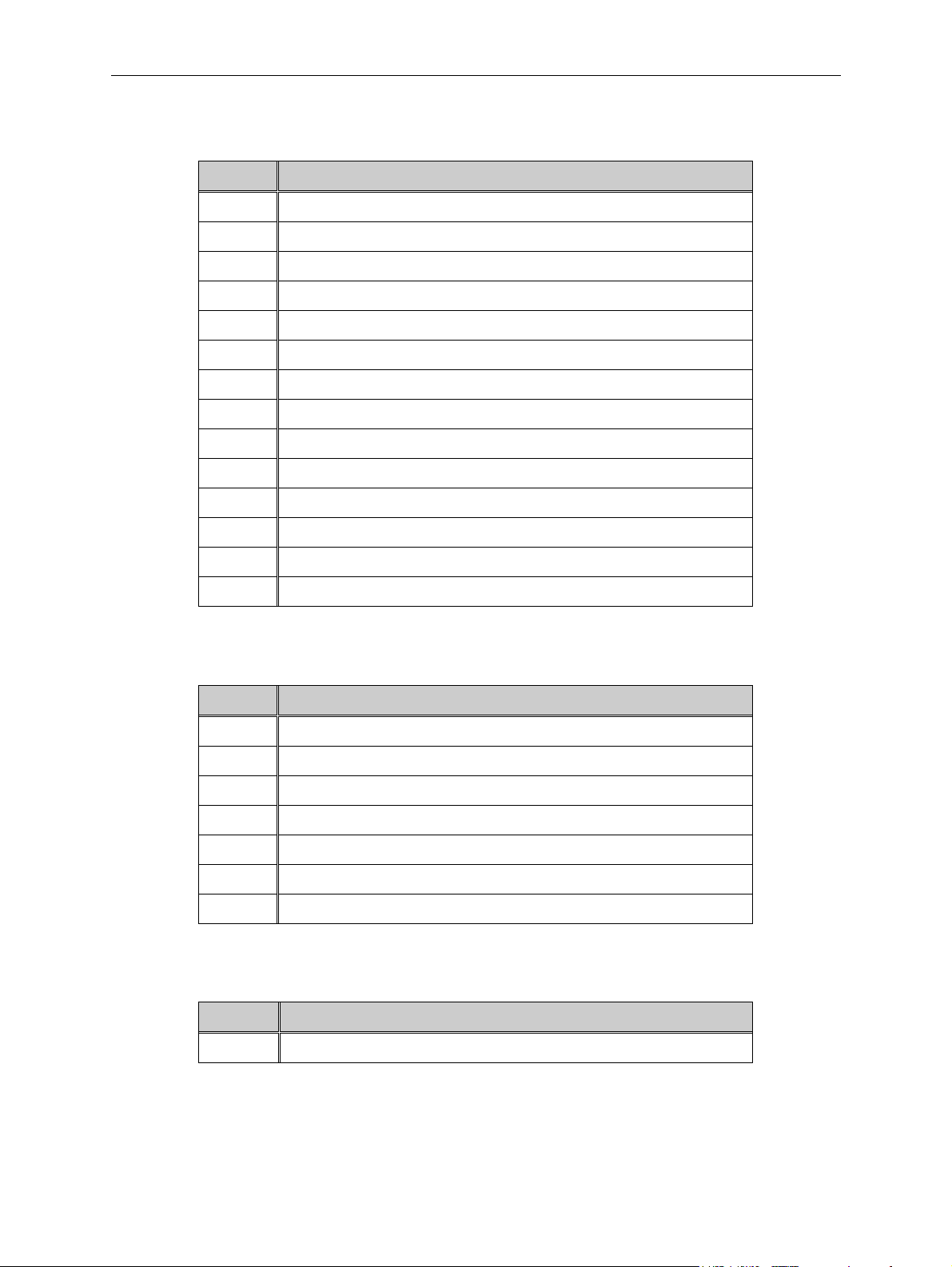
The following error codes are supported.
Table 15: Error Codes
Code Error
1
2
3
6
8
14
15
17
23
24
25
27
28
254
The following fault codes will be supported.
Reject coin
Inhibited coin
Multiple window ( ambiguous coin type )
Accept sensor timeout
2nd close coin error ( coin insertion rate too high )
Accept sensor blocked
Sorter opto blocked
Coin going backwards
Credit sensor reached too early
Reject coin ( repeated sequential trip )
Reject slug
Games overloaded
Number of coin meter pulses overloaded
Coin return mechanism activated ( flight deck open )
Table 16: Fault Codes
Code Fault
1
2
3
4
8
22
34
The following status codes will be supported.
EEPROM checksum corrupted
Fault on inductive coils
Fault on credit sensor
Fault on piezo sensor
Fault on sorter exit sensors
Fault on thermistor
Temperature outside operating limits
Table 17: Status Codes
Code Status
1
Coin return mechanism activated ( flight deck open )
Money Controls 2005. All rights reserved.
Page 41 of 50
Page 42
SR3 Type 1 Technical Manual TSP005.doc Issue 5.0 – Jan 2005
25. ccTalk Interface Circuits
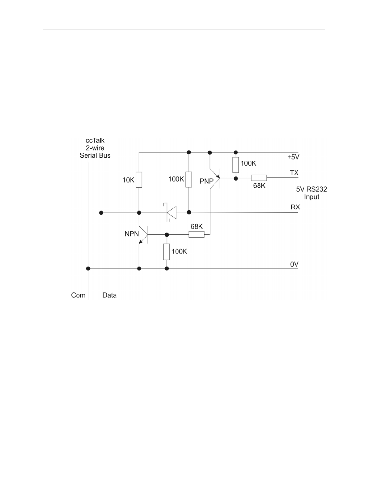
25.1 Circuit 1 – ccTalk Standard Interface
This circuit uses an open-collector transistor to drive the data line and a diode protected
straight-through receiver.
Figure 19: Circuit 1, ccTalk Standard Interface
Typical Components
Diode BAT54 Schottky Diode, low forward voltage drop
NPN BC846B High gain, medium signal, NPN transistor
PNP BCW68 High gain, medium signal, PNP transistor
Money Controls 2005. All rights reserved.
Page 42 of 50
Page 43
SR3 Type 1 Technical Manual TSP005.doc Issue 5.0 – Jan 2005
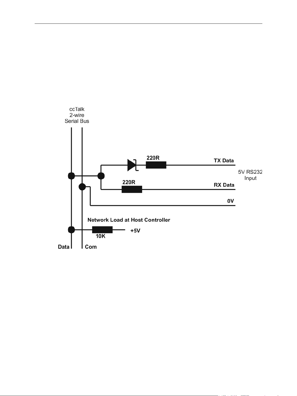
25.2 Circuit 2 – ccTalk Low Cost Interface
Assuming that the transmitting device is capable of sinking a reasonable amount of current,
a direct diode interface can be used rather than a full transistor interface. Although cheaper
to implement, this circuit does not have the drive capability or the robustness of other
designs.
Figure 20: Circuit 2, ccTalk Low Cost Interface
Money Controls 2005. All rights reserved.
Page 43 of 50
Page 44
SR3 Type 1 Technical Manual TSP005.doc Issue 5.0 – Jan 2005
25.3 Circuit 3 – ccTalk Direct Interface
A very low cost solution is to interface a single pin on a microcontroller directly onto the
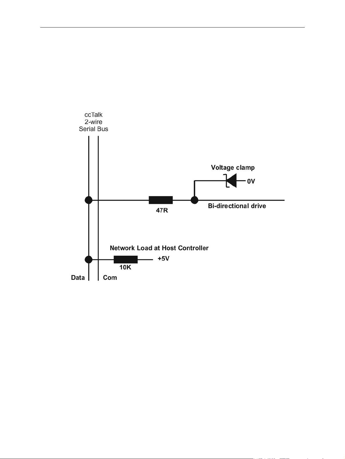
ccTalk data line. The pin can be switched between active-low for transmitting and highimpedance tri-state for receiving.
Figure 21: Circuit 3, ccTalk Direct Interface
Money Controls 2005. All rights reserved.
Page 44 of 50
Page 45
SR3 Type 1 Technical Manual TSP005.doc Issue 5.0 – Jan 2005
25.4 Circuit 4 – ccTalk PC Interface
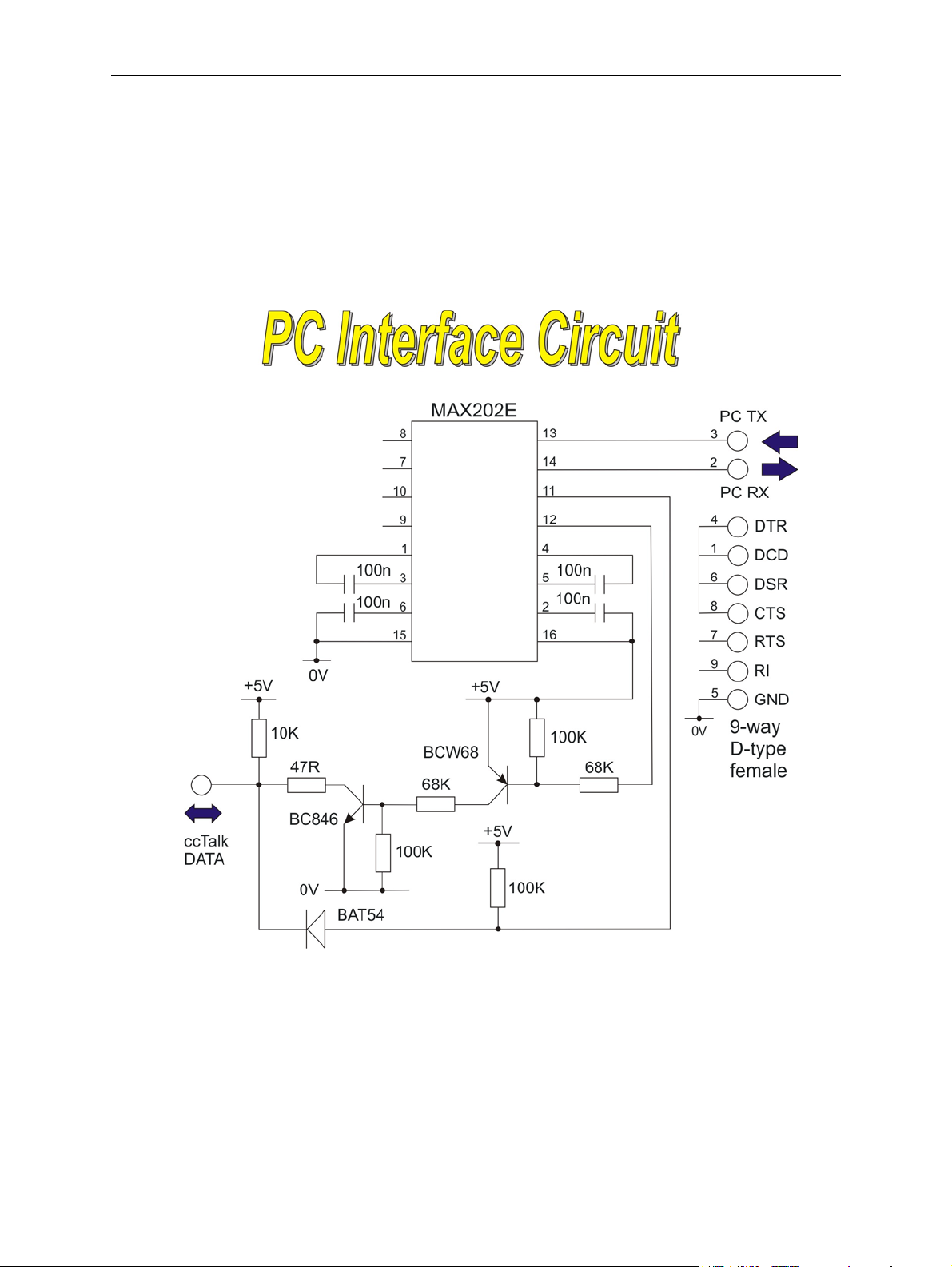
The circuit below shows how to connect the 9-pin serial port of a PC to the ccTalk data bus.
The only integrated circuit required is a Maxim level-shifter which operates off a single +5V
supply. Any small-signal diodes and transistors can be used.
Figure 22: Circuit 4, ccTalk PC Interface
Money Controls 2005. All rights reserved.
Page 45 of 50
Page 46
SR3 Type 1 Technical Manual TSP005.doc Issue 5.0 – Jan 2005
26. Fault Finding
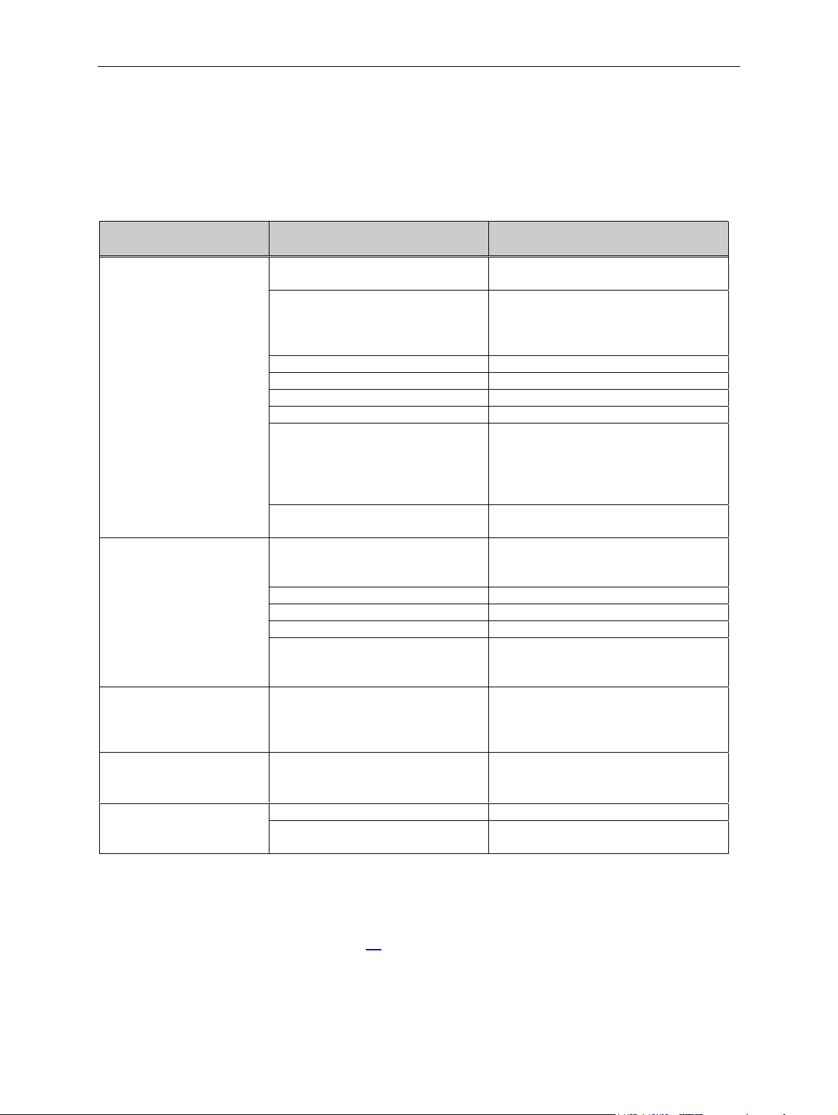
The following information is presented for customers’ guidance in rectifying a fault but
does not cover all possible causes.
All acceptors with electronic faults should be returned to Money Controls Ltd. or to an
approved service centre for repair.
Symptom Investigate Possible Cause
Acceptor does not
work
(all coins reject).
Poor acceptance of
true coins.
Coins stick or jam in
acceptor.
Connector.
Poor contact.
Loose wire.
Not switched on.
Power supply.
Incorrect voltage.
Inadequate current.
Rise time too slow.
Inhibit inputs. Acceptor inhibited.
Accept gate. Gate not free or dislocated.
Accept channel. Obstructed.
Reject gate. Not fully closed.
EEPROM checksum error
SR Sensor faulty
LED on rear cover is RED.
Credit opto’s faulty
Credit sensor blocked
Reject lever pressed
LED on rear cover is
YELLOW.
Remove the power and re-apply.
LED should be green.
7,8
.
7,8
6
.
7
.
9
Voltage less than 10V.
Power supply
(NB voltage drops when solenoid
is activated).
Accept gate. Gate not free or dislocated.
Connector. Loose.
Coin rundown. Dirty.
Both banks are enabled and
Bank select.
programmed with the same
10
coins
.
Rundown.
Accept channel.
Accept gate.
Dirty or mechanical damage.
Reject gate.
.
One of the true coin
types always rejects.
Label. Coin not programmed.
Connector. Loose or broken wire.
No accept signal.
6
This condition requires the SR3 to be reprogrammed.
7
These faults will only be seen if ‘Power-up Diagnostics’ is ON.
8
These faults require to SR3 to be returned for repair.
9
The SR3 will time out after 20 sec’s. Alternatively, switch the power off then on.
10
Refer to the MechTool section – page 15.
Accept channel.
Money Controls 2005. All rights reserved.
Page 46 of 50
Dirty or obstructed.
(acceptor time-out)
Page 47
SR3 Type 1 Technical Manual TSP005.doc Issue 5.0 – Jan 2005
27. Service
The coin rundown area should be cleaned regularly to ensure accurate discrimination of coins
and tokens. Only a damp cloth should be used.
Under NO circumstances should any solvent or foam type cleaner be used.
Access to the rundown is gained by opening the reject gate.
28. Electrical Interface Requirements
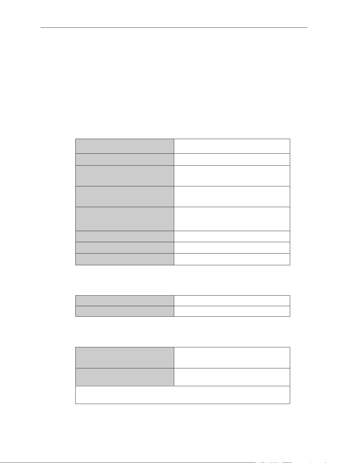
Table 18: Power Supply
Voltage:
Absolute:
Min / Max rise time:
Min / Max fall time:
Acceptor Power up time:
Ripple voltage [ < 120Hz ]:
Ripple voltage [ > 120Hz ]:
Ripple voltage [ > 1KHz ]:
Table 19: Current Consumption
Typically:
Maximum:
12V – 24V dc +/- 10%
Min 10V Max 28V
5ms / 500ms
(From 0V to within supply range)
5ms / 500ms
(From within supply range to 0V)
200 ms from the application of a valid
voltage supply. A valid supply must be
between the limits specified above.
< 1 Volt
< 100mV
< 20mV
70mA
450mA
Table 20: Environmental Ranges
Operating temperature range:
Storage temperature range:
(Recovery time by the acceptor after a temperature step change is 1 hour per
20°C. Maximum operating rate of change 20°C per hour.)
Money Controls 2005. All rights reserved.
Page 47 of 50
0°C to 60°C 10% to 75% RH
non-condensing
-30°C to 70°C 5% to 95% RH noncondensing
Page 48

SR3 Type 1 Technical Manual TSP005.doc Issue 5.0 – Jan 2005
29. Specified EMC Performance
29.1 Emissions
This product is compliant with EMC test specification EN55014-1; 1993
29.2 Immunity
This product is compliant with EMC test specification EN55014-2; 1997
29.3 Shock / Vibration Immunity
This product is compliant with BS 2011 part 2.1.[ IEC 68-2-27 ]
Money Controls 2005. All rights reserved.
Page 48 of 50
Page 49

SR3 Type 1 Technical Manual TSP005.doc Issue 5.0 – Jan 2005
30. Appendix A – Available Parallel Interface Looms
Table 21: Available Parallel Interface Looms
Loom Length Spares Part Number
SR3 loom assembly 220mm PSP12005
SR3 loom assembly 250mm PSP12003
SR3 loom assembly 400mm PSP12002
SR3 loom assembly 500mm PSP12004
SR3 loom assembly 520mm PSP12006
SR3 loom assembly 550mm PSP12022
SR3 loom assembly 650mm PSP12023
SR3 loom assembly 850mm PSP12007
SR3 loom assembly 3000mm PSP12061
Money Controls 2005. All rights reserved.
Page 49 of 50
Page 50

SR3 Type 1 Technical Manual TSP005.doc Issue 5.0 – Jan 2005
This manual is intended only to assist the reader in the use of this product and
therefore Money Controls shall not be liable for any loss or damage whatsoever
arising form the use of any information or particulars in, or any incorrect use of the
product. Money Controls reserve the right to change product specifications on any
item without prior notice
Money Controls 2005. All rights reserved.
Page 50 of 50
 Loading...