

Page 1

EPT-1409NF
EPT-2109NF
EPT-2119PF
SERVICE MANUAL
1
Page 2

Contents
1. Safety Instructions ( 2 )
2. Signal Block Diagram ( 4 )
3. Adjustment Test ( 6 )
4. Trouble Shooting ( 9 )
5. Spare Part list ( 14 )
6. Circuit Diagram ( 15 )
1. Safety Instructions
1.1 X-ray Radiation Precaution
Excessive high voltage can produce potentially hazardous X-ray radiation.
To avoid such hazards, the high voltage must not be above 31.0KV(14")
or 35.0KV(21") under any conditions. The normal value of the high
voltage of this television is 22.5KV(14") or 26.5KV(21") at max beam
current (maximum brightness) under a 90-260V, 50/60H
source.
1.2 Safety Precaution
WARNING:
Service should not be attempted by anyone unfamiliar with the necessary
precautions on this television. The followings are the necessary
precautions to be observed before servicing.
AC power
Z
1). Since the chassis of this television is directly connected to the
AC-power line (HOT chassis), an isolation transformer should be used
2
Page 3

during any dynamic service to avoid possible shock hazard.
2). Always discharged the picture tube anode to the CRT conductive
coating before handing the picture tube. The tube is highly evacuated and,
if broken, glass fragments will be violently expelled. Use shatterproof
goggles and keep picture tube away from the body while handing.
3). When replacing a chassis in the cabinet, it always is certain that all the
protective devices are put back in place, such as non-metallic control
knobs, insulating covers, shields isolation resistor-capacitor network, etc.
4). Before returning the set to the customer, always perform an AC
leakage current check on the exposed metallic parts of the cabinet such as
terminals, screws, metal overlays control shafts, etc., to insure that the set
is safe to operate without danger of electrical shock.
1.3 Product Safety Notice
Many electrical parts in this chassis have special safety-related
characteristics. These characteristics are often passed unnoticed by a
visual inspection and the protection afforded by them cannot necessarily
be obtained by using replacement, rated for higher voltage, wattage, etc.
Replacement parts with special safety characteristics must be identified in
this manual and its parts list. Before replacing any of these components,
read the parts list in this manual carefully. The use of substitute
replacement parts that do not have the same safety characteristics as
specified in the parts list may create shock, fire, X-ray radiation of other
hazards.
1.4 Automatic Degaussing
A degaussing coil is mounted around the picture tube, so that external
degaussing after mobbing the TV should be unnecessary. But the receiver
must be properly degaussed upon installation. The degaussing coil
operates for about 1 second after the power is switched ON. If the set is
moved or turned in a different direction, the power should be OFF for at
least 15 minutes. If the chassis or parts of the cabinet become magnetized,
poor color purity will result. If this happens, use an external degaussing
coil. Slowly move the degaussing coil around the faceplate of the picture
3
Page 4

tube, the sides and the front of it, slowly withdraw the coil to a distance
of about 6 feet before turning power OFF.
4
Page 5
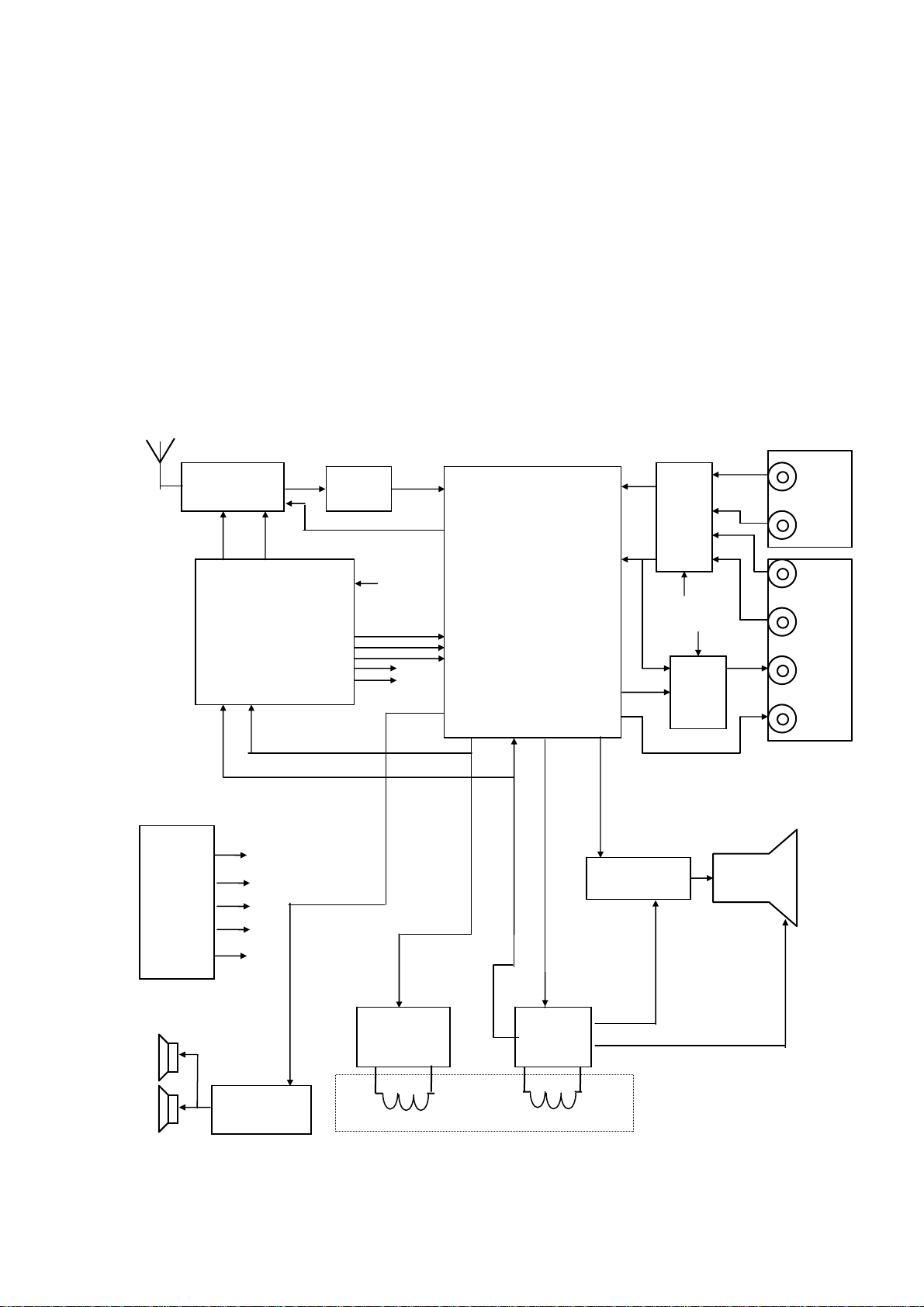
2. Signal Block Diagram
V
ter
This chassis is consisted of main chip LA76812 controlled by Sanyo
2
C bus and CPU LC863232A.
I
LA76812 is a performance and quality IC including PIF, SIF, AFC,
V/C/D, etc circuits.
TDA7056B used in BTSC sound system is a power amplifier.
CXA2104S is a BTSC decode function IC.
LA4225A used in MONO sound system is another power amplifier
LA78040 is used for vertical power amplifier.
The block diagram with MONO sound system is shown as follows:
FS
TUNER
SAW
Fil
SDA1 SCL1
Video
N101 CPU
LA863232A
R/G/B OUT
H V
SDA0
SCL0
AV1/AV 2
TV./AV
Select video
IF IN Ext VIDEO IN
RF AGC
Ext AUDIO IN
N201
LA76812
R/G/B IN
SDA
SCL
TV audio
AUDIO OUT Select Video
V OUT FBP H OUT R/G/B
N801
4053
AV1/AV 2
N305
4053
TV/AV
POWER
UNIT
110V
27V
17V
12V
8V
CRT PCB
SCREEN/
FOCUS
CRT
HV
V IN N401
LA78040
H IN
H OUT
N601
LA4225A
DY
Video1
Audio1
Video2
Audio2
A-out
-out
5
Page 6
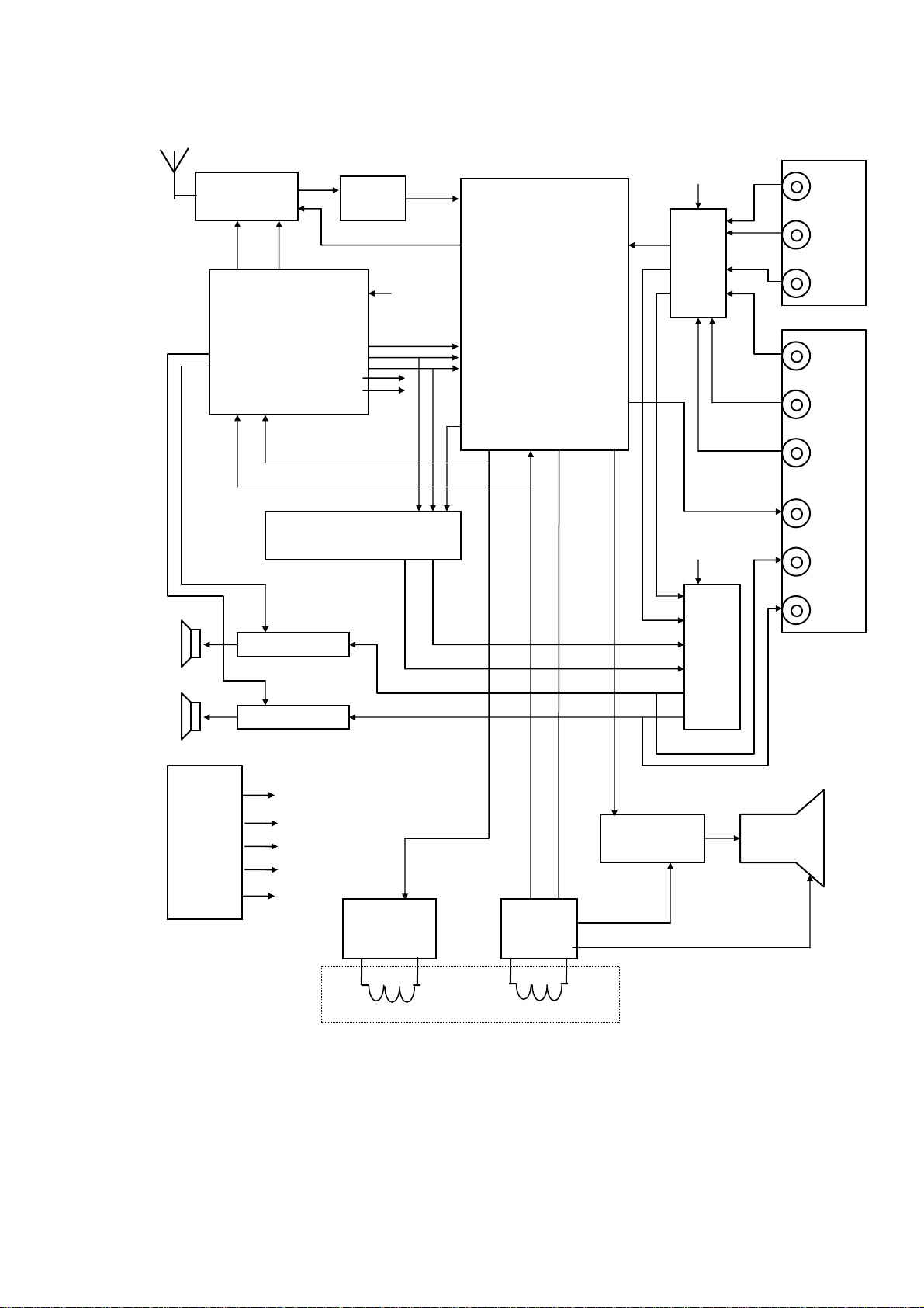
The block diagram with BTSC function is shown as follows:
ter
R
V
R
N
N
R
FS
TUNER
SDA1 SCL1
Video
N101 CPU
LA863232A
R/G/B OUT
Volume-R SDA0
Volume-L SCL0
H V
AV1/AV 2
SAW
TV./AV
Fil
Select video
IF IN
RF AGC Ext VIDEO IN
N201
LA76812
R/G/B IN
SDA
SCL
Select V ideo
TV Audio
V OUT FBP H OUT R/G/B
N307 CXA2104S ---------
TV-L TV-R
L
304 TDA7056B
304 TDA7056B
POWER
UNIT
110V
27V
15V
12V
8V
V IN N401
LA78040
H IN
H OUT
DY
CRT PCB
SCREEN/
FOCUS
AV1/AV 2
N801
4053
A-L
A-R
TV/AV
N305
4053
A-L
A-R
Video1
A1-L
A1-R
Video2
A2-L
A2-
-out
L-out
-out
CRT
HV
6
Page 7
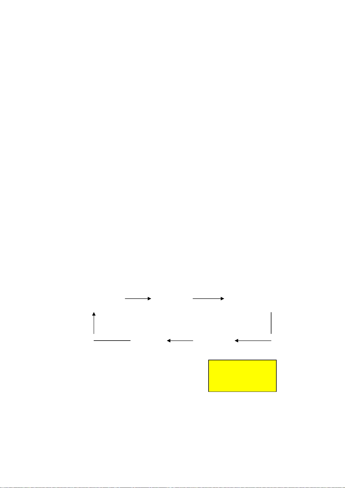
Nota: si no puede entrar con recall intentelo con disply o mute.
3. MENU TECNICO
3.1 PRUEBA DE AJUSTE
3.1.1 METODO DE ACCESO AL MODO DE SERVICIO
Usando el control remoto realize los siguientes pasos:
1. presione la tecla RECALL del control remoto y la tecla volumen
menos(V-) en el TV al mismo tiempo”.Aparecera en la pantalla del
TV la palabra FACTORY, indicando que se encuentra en modo
de servicio.
2. Para ingresar al modo de B/W (blanco balance)vuela a presionar
RECALL en el control remoto y volumen menos en el TV al
mismo tiempo
3. Para los ajustes de color, vertical, vuelva a presionar RECALL en
el control remoto y volumen menos en el TV al mismo tiempo
4. Para volver a la posición original de TV presione la TECLA
RETURT en el control remoto y apague el TV.”.
SETUP ADJUST
NORMAL TV FACTORY B/W Balance
3.1.2 MODO DE AJUSTE DEL BLANCO BALANCE B/W.
B/W Balance
a. Line Mode
Después de estar en el modo de servicio ,UD puede RGB bias, presionado
"0" para decrecer "S-BRI"; presionando "1" para incrementar " S-BRI ".
Presionando "2" para decrecer "R-BIA"; presionando "3" para
incrementar "R-BIA". Presionando "4" para decrecer "G-BIA";
presionando "5" para incrementar "G-BIA". Presionando "6" para
7
Page 8
decrecer "B-BIA"; press "7" para incrementar "B-BIA".
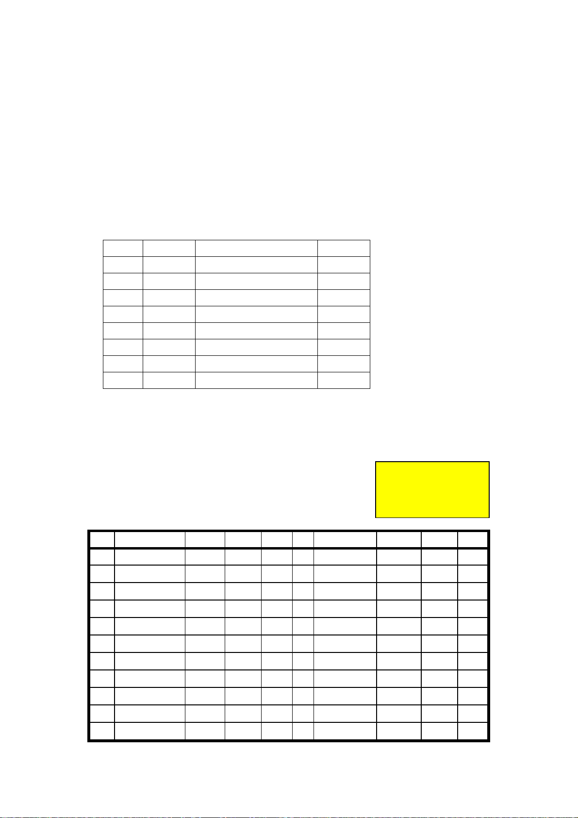
b. B/W Balance Adjusts
Después de ajustar RGB bias a, presione "Mute" para retornar al modo
" B/W BALANCE ", entonces presione CH+ or CH- para seleccionar
los item de la tabla de " B/W BALANCE ", presione VOL+ or VOL- para
seleccionar los item.
B/W ADJUST
1 S-BRI Sub-Brightness 0~127 2 C-B/W C-B/W 0~3 3 B-DRV B-Driver 0~127 4 G-DRV G-Driver 0~15 5 R-DRV R-Driver 0~127 6 B-BIA B-Bias 0~254 7 G-BIA G-Bias 0~254 8 R-BIA R-Bias 0~254
2). ADJUST Mode (Preset related to tube used)
En el modo "ADJUST", ud puede ajustar size, picture position, sub
picture status, OSD position, AGC status etc. , press CH+ or CH- to select
items in the " ADJUST " Table, press VOL+ or VOL- to adjust selected
item.
ITEM .00
H.PASE 8
ADJUST
ADJUST
Item Range Preset Note
Item Range Preset Note
00 H.PHASE
01 NT.H.PHASE
02 H.BLK.LEFT
03 H.BLK.RIGHT
04 V.SIVE
05 V.LINE
06 V.POSI
07 V.SC
08 NT.V.SIVE
08 NT.V.LINE
10 NT.V.POSI
8
0~31
0~31
0~7
0~7
0~127
0~31
0~63
0~31
-31~31
-31~31
0~63
11 11 NT.V.SC
2 12 RF.AGC
7 13 VOL.OUT
7 14 OSD H.POSI
73 15 OSD V.POSI
12 16 INPUT LEVEL
22 17 SPECTRAL
6 18 WIDEBAND
-02 19 STEREOVCO
-02 20 SAP.VCO
26
0~31
0~63
0~127
0~63
0~63
0~15
0~63
0~63
0~63
0~63
-02
20
100
25
13
08
26
25
1
51
Page 9
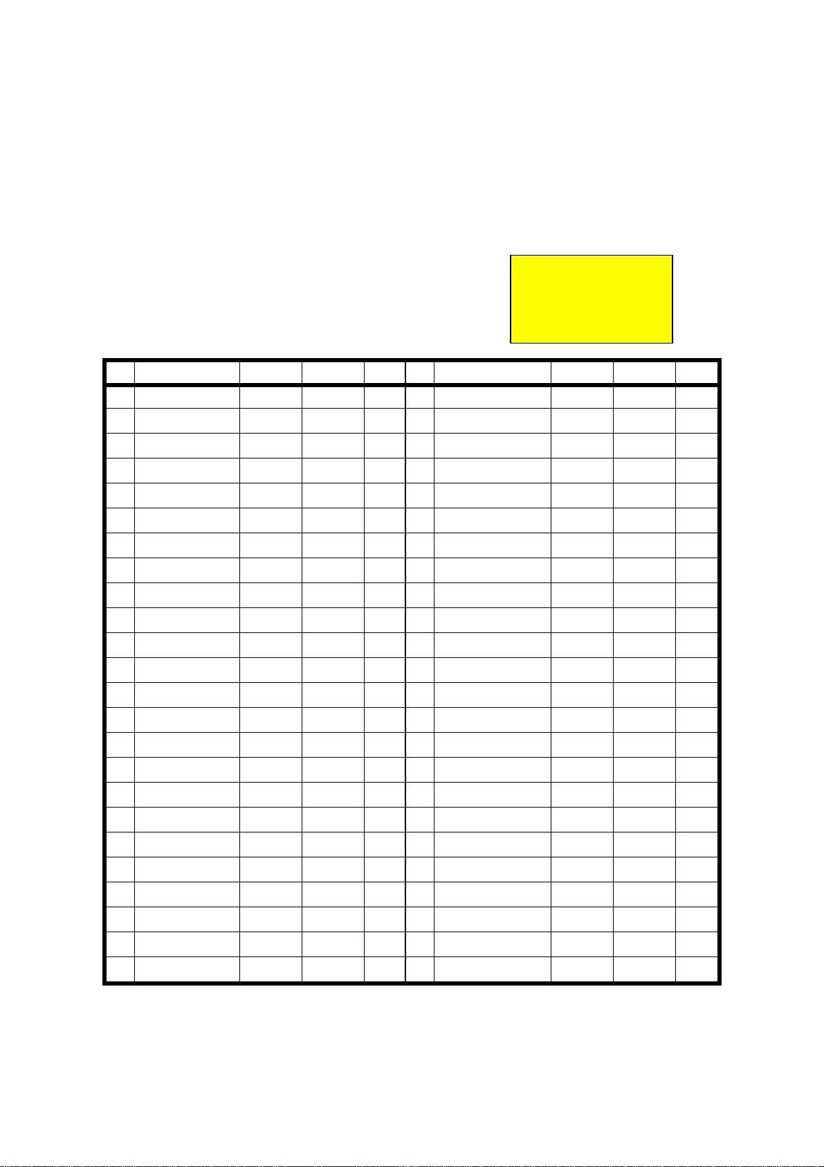
R
4). SETUP Mode
En el modo "SETUP", you Ud puede seleccionar las opciones, AV/TV
opcion, OSD opcion, power ON/OFF opcion etc. , presione CH+ o CHpara selecionar los item de la Tabla del " SETUP " ,presionando VOL+ o
VOL- para seleccionar los ajustes .
ITEM .06
BLK.STR.DEF 0
SETUP
SETUP
ITEM RANGE PERSET NOTE ITEM RANGE PERSET NOTE
LA76814/LA76812
00
01 SAP IC SELECT
02 SUB CONT
03 SUB CORLOR
04 SUB SHARP
05
06
07
08 V. SETUP
09 CD.MODE
10 DIGITAL OSD
11 OSD CONT
12 GRAY MOD
13
14
15 FBDBLK.SW
16 BRIGHT.ABL.TH
17 EMG.ABL.DEF
18 BRIGHT.ABL.DEF
19 MID.STP.DEF
20 R-Y/B-Y G.BL
21
22 C.KILL.OFF
23 SND.TRAP
SUB TINT
BLK.STR.OEF
AFC GAIN
B.GAM.SEL
RG.GAM.DEF
-Y/B-Y. ANG
0~1
0~1
0~31
0~63
0~63
0~63
0~3
0~1
0~1
0~7
0~1
0~127
0~15
0~15
0~15
0~15
0~1
0~15
0~15
0~3
0~15
0~15
0~1
0~1
1 24 VOL.FIL.OFF
1 25 VIF.SYS.SW
31 26 VIDEO.LEVEL
25 27 FM.LEVEL
31 28 POWER OPTION
31 29 POWER FLAG
0 30 SEARCH CHECK
1 31
1 32 AV.OPTION
0 33 POSION L/R
0 34 BLUE.BACK
55 35 BLACK.BACK
1 36 STEREO OPTION
3 37 WOOF/H.PHONE
1 38 WOOF VOL.OPT
1 39 SENSITIVITY
6 40 V.MUTE P.OFF
1 41 CCD OPTION
1 42 V-CHIP OPTION
1 43 PASS WORD.DPT
15 44 COMB.OPTION
15 45 TUNER OPTION
0 46 GAME OPTION
0 47 SCREEN OPTION
SEARCH SPEED
0~1
0~3
0~15
0~31
0~3
0~1
0~1
0~1
0~3
0~1
0~1
0~1
0~1
0~1
0~1
0~1
0~1
0~1
0~1
0~1
0~1
0~1
0~1
0~1
0
1
7
25
0
0
0
1
2
1
1
1
1
0
1
0
0
1
1
1
0
1
1
1
9
Page 10
r
pply
N
4. Trouble shooting
Rectifying and Powe
Detection
Rectifying and
Detection
Rectifying and
Detection
Rectifying and
Detection
T601
14
9
12
13
10
12
9
18/15V
Amplifying
N603 7812
N605 7805
15V
N602 78L05
CPU
Power Su
110V
27V
H Drive
Power Supply
Power Supply
H.OUT
V.OUT
Power supply
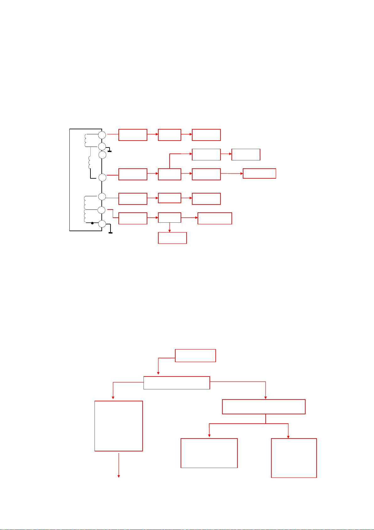
Complete set power supply outline
4.1 No grating, no picture, no sound
General, these failures are produced by power sources, because of which
refer to a wider area, so that can be divided them two conditions to
explain: no +B 110 V and existing +B 110V.
(1) No +B (110V) voltage (voltage of network AC 90~260V )
These failures may be caused by power supply switch.
Check fuse F601 or 602
Y
Check C607,
C603~C606,
V613 at
condition of
short-circuit?
Check voltage +B
=0V
Check voltage on D pole of V613
(switching MOSFT)
Check 90~260V AC input
and R602 VD603~VD606
rectifying, V613.
Y N
=200~310V
Y
Check if any
diodes of VD621~
VD624 is
10
Page 11

Replace the parts of
failure
11
Page 12
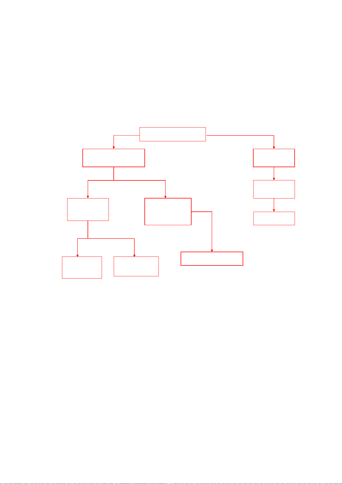
(2) Existing +B 110 V
N
These failures may be caused by abnormal operation of horizontal
scan, to confirm which can observe the filament of tube whether bright on.
If determined horizontal scan in abnormal operation, look for the failure
start from the horizontal drive stage. Search upward to LA76812 with
method of checking DC voltage and waveform according to sequence:
PIN27/H.OUT port→ PIN25 power supply→VD622 output.
Check if the out waveform of
Pin27 is correct?
Y
Check V501, T501
and connected
components.
Y
Check if the voltage at pin25 of
N201 is 5V?
Check if the BUS is
connected correctly?
Then check N201.
N
Y
Check horizontal
output stage and
deflection circuit
Check filament
circuit of FBT~CRT
N
Check the CPU operating.
Check the resistor
R503.
Check if connected
Components is
short-cut to GND?
N
Check VD622
12
Page 13
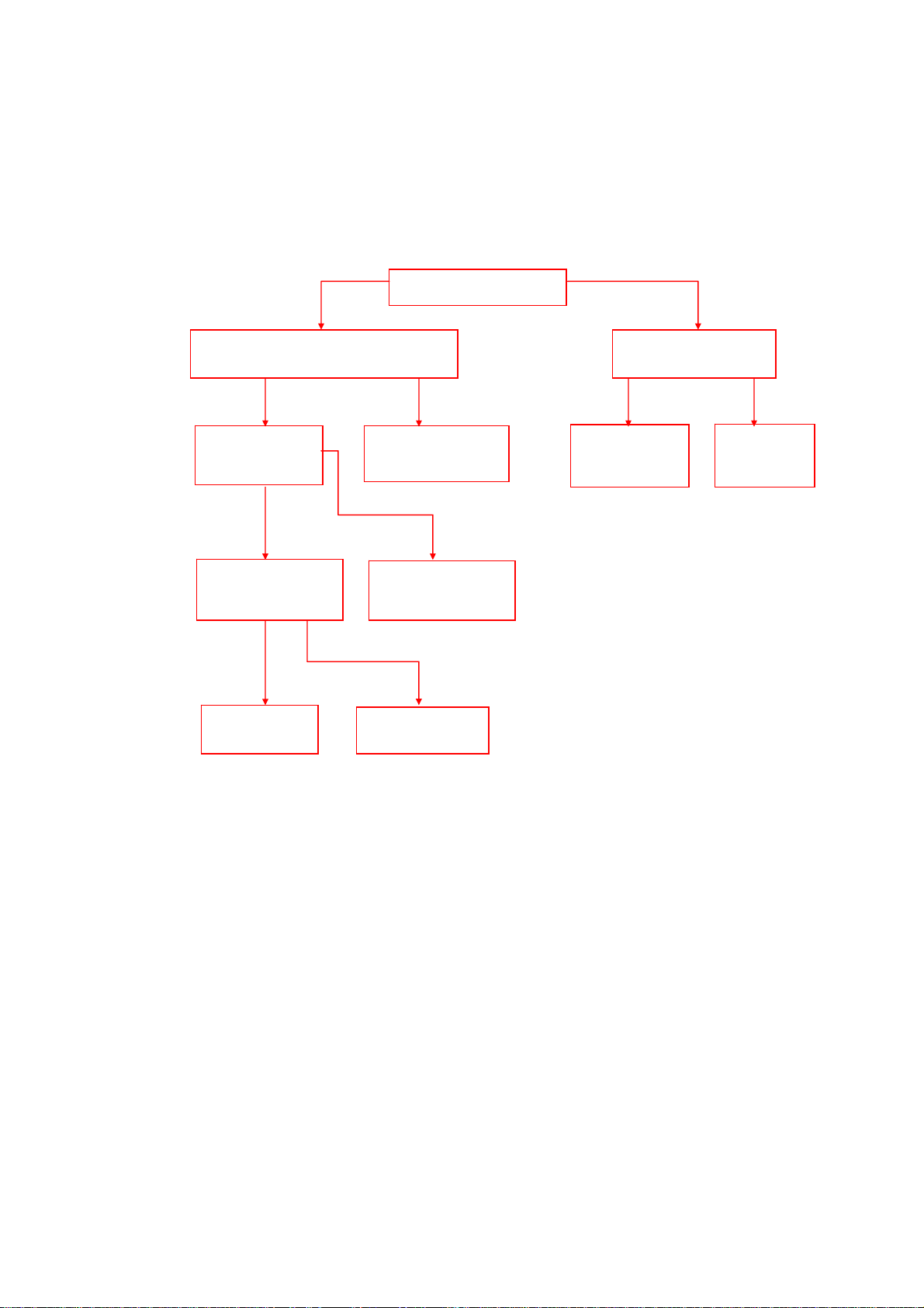
4.2 Existing grating and no picture
Because of the picture video signals and OSD characters display are input
from PIN44, PIN15, PIN16, PIN17 of LA76812(N201), so to observe
characters on screen of faulted TV can determine the approximate area of
fault.
Display OSD characters on screen
When searching automatically channels, check
CVBS waveform existed at N201/PIN44
N Y
Check 180 V power supply on
CRT boar d
Y N
N Y
Check CVBS waveform
existed at N201/PIN44
Check operating status of
TUNER and connections
Check bus between
N101, N102, N201*
Check 180 V
power supply of
relative plug-in
Y
N
Check CVBS waveform
at N201/PIN19/PIN20/
PIN21
Check circuit between
PIN44~PIN46 of N201
Y
N
Check CRT board
If the ABL circuit is OK,
then check N201
*:Whenever open or interconnect on
2
the BUS from CPU to E
PROM and
4.3 Existing grating, no picture and sound
Processing according “4.2 Existing grating and no picture” at first, let the
picture display normally, then check sound. About the repair method, see
“4.4 Existing grating and picture, no sound”.
13
Page 14
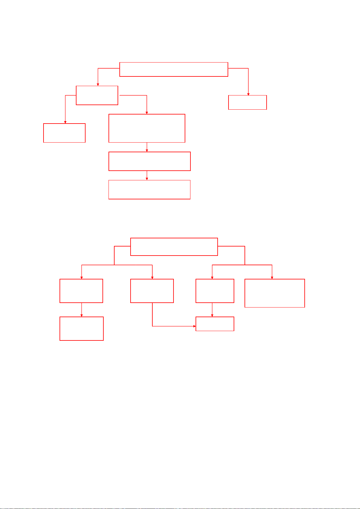
4.4 Existing grating and picture, no sound (with BTSC function)
N
k
Check two pins of loudspeaker whether normal
Y
Check the
loudspeaker and its
connection
Y
Check waveform
output from N303
and N304
Check external element connected to
N303 N304, specially supply power,
volume control from CPU and input
signal from N305 (TV/AV selecting)
Check the sound signal input pin2,
pin12, output pin14, pin15 of N305
Check N307 signal input pin11,
BUS, power supply and connections.
4.5 Cannot save channels
Y
N
When searching automatically channels,
observe whether can display picture
N
Check
loudspeaker
ote: Mono sound circuit is
much easy for repairing
referencing the bloc
diagram.
N
N
Y
Check AFT voltage
variation at
N101/PIN14
Y
Check BUS
connected to N102
and N102
Check voltage
variation at
N201/PIN46
N
Check the signal
from IF to N201
pin5 and pin6
Check N201
Check TUNER power supply
5V, 33V, RF AGC to N201
and BUS connection.
14
Page 15
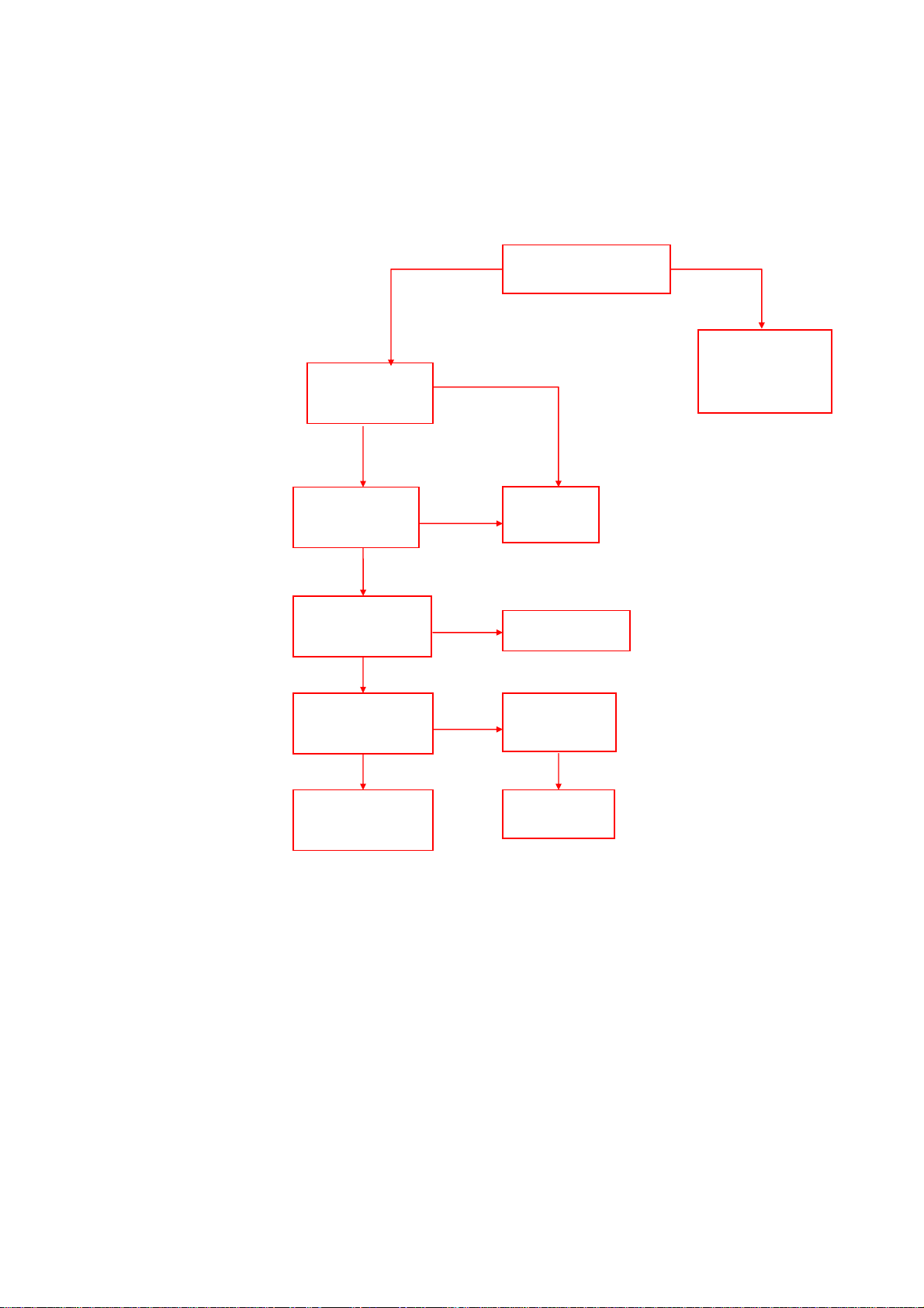
4.6 CPU non-operating
Check voltage at
N101/PIN17
(RESET)=5V
Y
Manual RESET than
OK?
N
Check oscillating
waveform at
N101/PIN10/PIN11
Y
Check the voltage at
N701/PIN13 is fixed
except 0V
Y
Check voltage at
N101/PIN12=5V
N
N
Check 15V~CPU 5V
Supply mainly R625 and
connected components.
Check V102 and
Y
N
N
Y
VD103 RESET
circuit
Check transistor
oscillating outer
elements
Check the BUS
connection
Check whether any
functional keys of the TV
always be pressed
Check N101
15
Page 16

5.The component that will be shattered listing
V501 2SC2383-O
V502 2SD1555/2SD1556/2SD2539
V613 2SC4236/2SC4237/ KA5Q1265RF
N201 LA76812/LA76814
N101 LC863232A-5V57
N102 AT24C04
N1101 HS0038A
N306 LA4225A / N303 N304 TDA7056AQ
N401 LA78040/LA7841/LA7845
N604 PC817
VD110 CW574CS
U101 STUF770(FS)/TEDH9-237A
T502 BSC24-33553-6P/ BSC25-3355-8/BSC29-3802-13R
T601 BCK-70-01C/BCK-180-408X
N602 N603 N605 KA7805/KA7812
T501 TX0040 /BCT-16
Speaker 5W-8Ω/5W-16Ω/10W-8Ω
16
Page 17
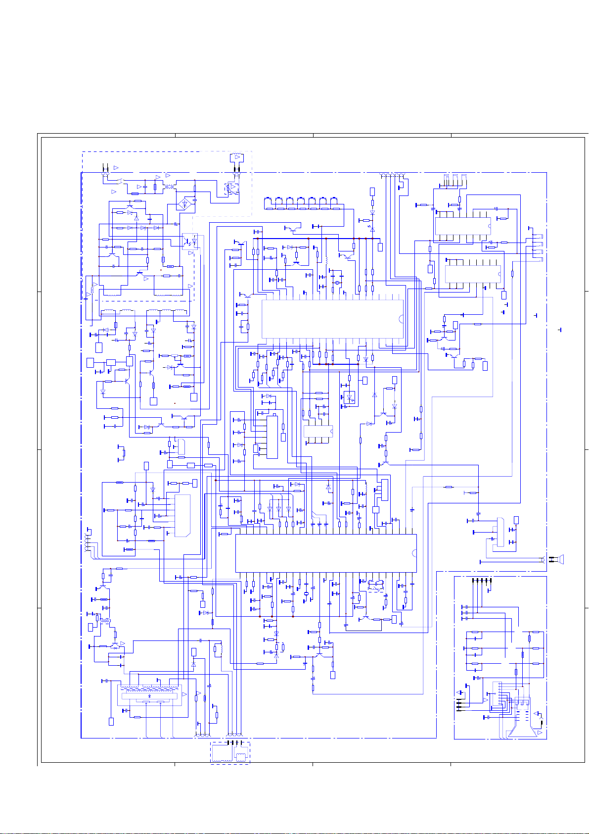
.
6
Circuit Diagram
!
XS601
1
2
SW601
KA04
!
F601
3.15A 250V
R615
5.6K¦¸
VD611
R608
17V
B2
C125
470uF
BGR
V501
2SC2383(D,R)
2
160V
V601
2SB892
1.8K
HZ7C1
VD609
R607
1K¦¸
IN4148
R610
22K¦¸
C612
R613
R614
2.7K¦¸
0.012
22
V602
2SC3807
C614
0.015
V613
2
VD621
RGP 15D
500V
R504
1K¦¸
R506
1K¦¸
T501
R507
270
TX-0004
FB502
LF-05
2SC4236/7
1
14
13
R624
3W1
C621
C623
C624
470
470
25V
1000¦ÌF
2
R625
1
N602
15V
B5
78L05
R642
10k¦¸
V646
R671
1.2K¦¸
2SB892
VD634
IN4148
R672
330K
R649
560K
C635
0.47
POWER GND
FB503
HOR.GND
LF-05
R432
1.2K¦¸
R402
3.3K¦¸
C403
1000
R404
R403
2
10K¦¸
2.2
R411
18K¦¸
C408
R405
560
3.3¦ÌF
R412
35V
22K¦¸
C414
1000¦ÌF
R431
1.2K
R504A
680
100V
C509
0.056
H.PRE-DRIVE
C508
1000
FB501
LF-05
!
V502
C511
H.OUT
D1555
1.6KV 2KV
7200
C512
2700
C508
T502
10 8
2
10¦ÌF
C519
63V
0.1
R514
+110V
1K¦¸
D
!
R619
12M
!
C615
2200P
AC400V
C622
25V
1000uF
+5V-1
C
B
A
XS701
12345
500V
C506
3900
500V
35V
C507
47¦ÌF
+27V
!
VD622
RGP 10D
35V
VD610
RGP 10D
!
!
AC275V
L601
R601
C601
220K¦¸
0.22
LF-003
VD603-VD606
TVR4J
+
_
VD608
C611
IN4148
0.1
C618
500V
R639
R673
3.9K¦¸
VD645
HZ5C1
C404
1000¦ÌF
1
C607
4700
VD612
400V
150¦ÌF
IN4148
R609
15k¦¸
5
R603
22
!
7
12
C625
470
C626
330
2
12K
R634
10K¦¸
V647
2SB892
R618
1W0.47
B4
27V
R670
2.2K
+27V
C409
0.022
C407
R406
100V
1
0.1
R407
330
VD623
RGP 10D
35V
V642
2SC1815
VD401
35V
RGP10D
C405
100¦ÌF
C406
1¦ÌF
R618
120k¦¸
R617
120k¦¸
R604
5
22
9
R644
5.6K¦¸
VD633
W6V2B2
C632
16V
470¦ÌF
N401
LA7840
N604
PC817D
C608
2KV
1000
1
10
1KV
R646
VR601
22K
2k¦¸
R621
100K¦¸
V643
2SC1815
R650
150k¦¸
R640
R645
47K¦¸
22K¦¸
V640
2SA1015
R643
R641
22K
10K
N603
12 3
2
R630
56
R761
KA7812
1
+12V
0.47
R410
R409
4.7K¦¸
4.7K¦¸
7654321
PNMP
VCC1
INV IN
NON-INV IN
VCC2
V OUT
GND
C433
1uF50V
76534
!
!
T601
11
C629
470
160V
C628
220¦ÌF
2
N605
7805
V.DEF.OUT
R518
56K
R452
3.9K
!
SC
FO
HV
HV
FO
SC
C316
25V470¦ÌF
4
C806
10¦ÌF
R810
82
VIDIO2
R819
1234567
A-R
R811
75
A-in A-out
VIDEOOUT
D
+5V-1
C
LA4225
+17V
123 45
C317
1000¦ÌF
C318
0.01
12345
GND
CRT
HVFOSC
XS306
2
XP306
1
R901
2
15K¦¸
R902
1.8K¦¸
R921
2
15K¦¸
R922
1.8K¦¸
R911
2
15K¦¸
R912
1.8K¦¸
CRT
!
B
A
321
L611
!
LM-01
XS602
XP602XP601
1
2
5
R602
3.9
1000V
C603~C606
1000
VD624
BYT 56M
+110V
B1
+5V
VD501
MTZJ8.2C
250V
C514
0.47
+187V
VD504
RGP10J
!
2
R520
3.6
HEATER
4
XS501
!
P10X180M
t
PS601
V103
R163
INVERTOR
2SC1815
33K¦¸
R119
10K¦¸
C113
0.01
V114
2SC1815
R118
27K¦¸
C138
100
R165
C139
100K¦¸
15
C218
3.3¦ÌF
R226
C219
8.2K¦¸
47¦ÌF
VD114
1
R503
390
MTZJ5.1B
2
R229
56
+5V
R453
3.9K
12V
R511
2.2
C773
470¦ÌF
C502
25V
63V
100¦ÌF
C504
C501
C505
1¦ÌF
R502
0.015
63V
63V
5.6K¦¸
0.01
C401
L502
LF-05
0.47
N201
R501
2728
LA76812
H APC FIL
H.OUT FBP IN
2K¦¸
VCD IREF
29303132333435363738394041424344454647484950515253
R757
R509
10K¦¸
R508
10K¦¸
1
R510
1K¦¸
160V
C515A
4.7¦ÌF
1
123
CN-DY
4.7K¦¸
C759
4.7¦ÌF
H.LIN.COIL
L501
037*
R524A
220K¦¸
432
1
XS502
C114
100
+33V
VCC(H/D)
CLOCK OUT
C758
0.01
C103
100
R116
4.7K¦¸
R121
1K¦¸
C402
0.22
R755
22K¦¸
R760
3.9K¦¸
C226
0.01
R117
10K¦¸
R120
1K¦¸
C719
100
RAMP ALC FIL
HDL VCC
N101
C115
LC8632325V57
100
R123
1K¦¸
C221A
0.01
R704
10K¦¸
16V
SW101P+SW103
R157
22K¦¸
R114
1M¦¸
C112
2.2¦ÌF
C111
0.033
H.SYN
V.SYN
R.OUT
G.OUT
C116
100
R122
1K¦¸
R125
1K¦¸
VD110
C126
UPC574J
10¦ÌF
A101
AGC SCL SDA BP BT GND IF
ST5UF770
16V
C774
1000¦ÌF
B
VD702
1N4148
AKB IN
V OUT
GND(CCD/H)
CCD FIL
C757
10¦ÌF
R748
1.2K¦¸
R749
1K¦¸
R756
C756
10K¦¸
1¦ÌF
R746
4.7K¦¸
C762
10¦ÌF
R156
9.1K¦¸
R115
100
R747
8.2K¦¸
CVBS-IN
B.OUT
R124
1K¦¸
B OUT
X-RAY
MTZJ12A1
VD757
VD756
RGP10D
SW102
SW104
SW106AVSW107
V604
NPN-1
R113
390K¦¸
FILT
OSD BLANK
R104
8.2K¦¸
R702
100
G OUT
XIAL
VOL+
R155
4.7K¦¸
V102
2SA1015
RESETNCKEY2
NC
R126
1K¦¸
VD721
MTZJ7.5C
VD704
1N4148
R UOT
DDS
C750
0.047
SW105
VOL-
R154
3.3K¦¸
R111
1.5K¦¸
R112
RESET
8.2K¦¸
SDA0
SCL0
C128
C129
220
220
C137
R128
220
220
R140
100
N102
AT24C04
R705
220
R
16V
C707
47¦ÌF
C706
R703
0.01
100
BL IN
VCC(RGB)
ACC FILTER
XIAL
R754
1K¦¸
C754
0.47
R759
12K¦¸
R708
100¦¸
C720
1¦ÌF
POWER
MENU
R153
R152
R151
2.2K¦¸
1.2K¦¸
820¦¸
C118
1000
V191
R109
10K¦¸
L101
2SC1815
39¦ÌH
10V
C108
C106
C10415C105
X101
0.1
15
470¦ÌF
C107
32KHz
R108
0.01
390K¦¸
GND
XTAL1
XTAL2
AFT IN
VDD
KEY1
ENABLE
S-VHS
SDA1
R188
22K¦¸
R129
220
R138
4.7K¦¸
R139
100
678
4 5
C704
1¦ÌF
B IN
CHROMA APC
C753
C752
16
2.2¦ÌF
X701
3.58MHz
R762
6.8K¦¸
C707
V701
100
2SC1815
R710
C809
330uF10V
R811
IR-IN
SCL1
NC
R186
R134
R185
22K¦¸
22K¦¸
22K¦¸
C100A
1000
R137
4.7K¦¸
C120
C100
C119
47¦ÌF
10¦ÌF 16V
0.01
123
VD706
1N4148
C705
R204
63V
100K¦¸
1¦ÌF
C207
0.1
R205
R206
C702
C703
100
100
1¦ÌF
1¦ÌF
BUS DATA
BUS CLOCK
ABL
R IN
G IN
SELECT V.OUT
GND(V/C/D)
VCC(V/C/D)
EXT V.IN
INT V.IN
C712
0.01
C713
16V
220¦ÌF
C811
1¦ÌF
R706
C213
100
1¦ÌF
16V
C715
R764
R763
100¦ÌF
27k¦¸
R709
33
+12V
P-
VD103
MTZJ3.6A
C110
0.01
C117
100
R127
1K¦¸
2
+110V
G
VD703
1N4148
R701
100
C755
1000
R758
12K¦¸
10K¦¸
XS001
6
12345
VIDEO2
STOP
SDA
SCL
VD111
1N4148
VD112
RM11C
R216
330
+5V-1
WOOFER VOL
AV1
VD108
1N4148
V108
2SA1015
C368
22¦ÌF
V302
MUTE
2SC1815
FL201 M1967D
12345
SAW FIL TER
L202
PIF IN
VCO COIL
GND
123456789101112131415161718192021
NC
50/60
ALARM
COMB FILTER
V/MUTE
TV/AV
424140393837363534333231302928272625242322
+15V
R142
100K¦¸
VD105
1N4148
C123
25V
100¦ÌF
R373
22K¦¸
R364
18K¦¸
R314
1K¦¸
C310
16V4.7¦ÌF
C201
C202
0.022
0.01
123456789
AUDIO OUT
FM OUT
PIF AGC
RF AGC OUT
PIF IN
EXT AUDIO IN
SND APC FIL
PIF APC
SIF OUT
SIF IN
54
C304
C303
8
63V
1000
C305
C209
0.01
R331
1¦ÌF
R207
3.3K¦¸
120
+12V
R215
330
C812
10¦ÌF
+12V
R141
390
R160
330
R105
10K
R183
R182
22K¦¸
22K¦¸
R193
R191
R192
1K¦¸
22K¦¸
1K¦¸
VOLUME-R
VOLUME-L
POWER
DEGAUSS
WOOF ON/OFF
MUTE
AV2
SRS
R189
R184
VD104
22K¦¸
22K¦¸
1N4148
+5V-1
R135
1K
N103
HS0038
VD107
MTZJ5.6B
R720
1K
L203
10¦ÌH
C205
R203
100K¦¸
16V
100¦ÌF
C204
0.01
C206
1¦ÌF
R202
33K¦¸
1011121314151617181920212223242526
IF GND
VCC(VIF)
FM FIL
AFT OUT
BLACK STRETCH FIL
VIDEO OUT
VCO COIL
VCO
C210
0.47¦ÌF
L204
VCO
R713
C714
560K¦¸
4.7¦ÌF
R208
1K¦¸
BUFFER
V203
2SA1015
VIDEO1
L1
R1
R813
C821
N801
10¦ÌF
4053
R194
10K¦¸
+5V-1
R179
22K¦¸
R187
1K¦¸
R837
6.8K¦¸
R834
220
R814
82¦¸
C808
10¦ÌF
89
V1
10111213141516
N305 TV/AV
89
4053
10111213141516
R357
+5V
C833
R835
10¦ÌF
V834
27K¦¸
2SC1815
C834
R836
V832
10¦ÌF
2SC1815
R345
4.7K¦¸
XP501
187V
GND
HEATER
XP-4
1234567
VIDEO
R1
R2L1V2
L2
L
R
C841
R818
10¦ÌF
T-R
LRT-L
A-L
R807
100¦¸
R178
+5V-1
22K¦¸
R839
R190
1K¦¸
1K¦¸
R346
3.3K¦¸
C330
C319
1¦ÌF
0.01
XP701
12VBG
R
C903
C913
100
C923
100
100
R905
330
C904
560
R925
330
C924
560
R915
330
C914
C931
560
250V
XS901
CRT-SOCKET
22¦ÌF
!
C941
2200 2KV
R820
7.5K
R181
6.8K¦¸
C101
4.7¦ÌF
R363
27K¦¸
1 2 3 4
17
Page 18

18
 Loading...