

Page 1

MITSUBISHI DIGITAL ELECTRONICS
V19 / V21
PWB Level
Troubleshooting Guide
Page 2

V19 / V21
PWB Level Troubleshooting Guide
©2002 Mitsubishi Digital Electronics
9351 Jeronimo Rd.
Irvine, CA 92618
All Rights Reserved
iiii
Page 3

Table of Contents
V19 / V21 PWB Level Troubleshooting Guide
Introduction iii
Printed Circuit Board Layout 1
TROUBLESHOOTING
Shut-Down Problems 2
X-Ray Protection Failures 3
Horizontal Deflection Failures 4
Vertical Deflection Failures 5
TV Microprocessor Diagnostics 6
Color or Video Failures 7
QUICK REFERENCES
Power Supply 8
Main Board 9
Deflection Jungle 9
3DYC Module 10
CRT Drive 10
2HDW Module 11
Digital Module Assembly 12
Convergence Module and IC 13
iii
iiiiii
WAVEFORMS
KH, DR, DQ Connectors 14
DQ, EF Connectors 15
EF, RM, EA Connectors 16
EA, EB, VA Connectors 17
VA, DB, VD Connectors 18
VD Connector & IC8C01 19
IC8C01 20
IC8C01, IC9A20, IC9A50 21
ii
ii
iiii
Page 4

V19 / V21 PWB Level Troubleshooting Guide
Introduction
The purpose of this V19 / V21 PWB Level Troubleshooting Guide is to assist the servicer to quickly identify common
chassis test points, and to facilitate efficient servicing procedures in the field or service shop / depot. It is intended for use
in tandem with the Service manual as an aid to troubleshooting a set. Included are many major DC voltage measurements
and AC waveforms pertinent to proper operations of the chassis. In addition, troubleshooting procedures are provided for
some common service issues a Technician may encounter.
This guide is not intended to be used as a resource for technical training, circuit analysis, or adjustment procedures. Refer
to the V19 / V21 Technical Training guide and/or the Service manual which includes all schematics, parts lists, and
adjustment procedures for these purposes.
iii
iii
iiiiii
Page 5
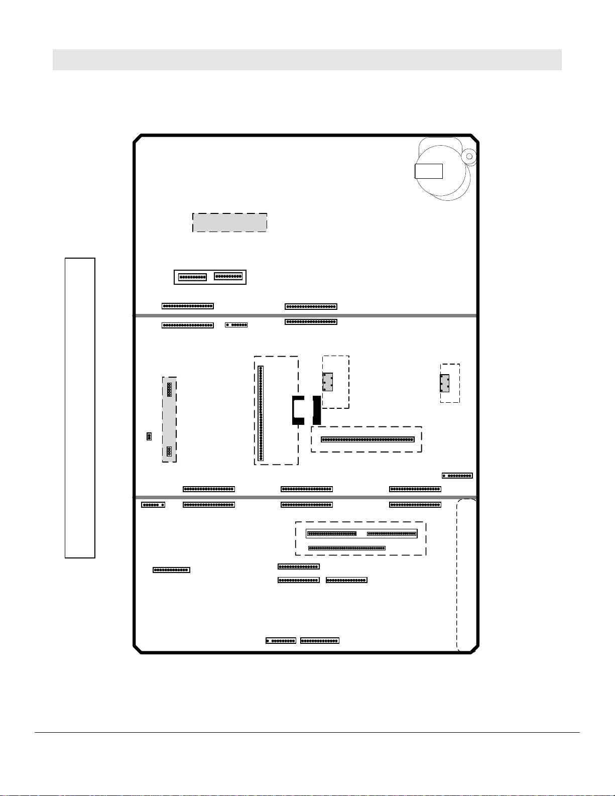
V19 / V21 PWB Level Troubleshooting Guide
DBF-PCB
Printed Circuit Board Diagram
RM
DR
KH KH
KKKA
SVM-PCB
FA
KE
PM
DQ
Jungle Module
KFKF
IC9A50
IC8C01
Heatsink As sy
KD
VD
Generator
Convergence
KC
2HDW-PCB
EB
Shield
Assembly
3DYC-PCB
EF
Shield
EA
IC9A20
Assembly
PF
VA
RF
DB
PCB-Signal PCB-Power PCB-Main
PCB Terminal
DA
1111
Page 6
V19 / V21 PWB Level Troubleshooting Guide
Troubleshooting
Shut-Down
Problems
Initial
Front Panel
L.E.D. Status
Power
Applied
Off
Problem in
Standby Power
Supply or TV
Microprocessor
is not running
Check Standby
Supplies
Page 8
Check TV
Microprocessor
IC7A00
Page 6
Fast Blink
70 Seconds
Only
Normal
Operation
If the Light Box is
removed from the
cabinet without the
front panel control
assembly, be sure to
wait 70 seconds prior
to turning on the TV.
There is no visual
indicator to remind you
of the delay while the
DM is in the process of
booting.
If Set Shuts
down after
power-up,
continue Shut-
Down
troubleshooting
Fast Blink
Continuous
TV
Microprocessor is
running, DM
failed to boot.
UnPlug Set, wait
30 seconds and
try again.
Replace DM
Assembly
Slow
Blink
Normal Operation
TV "On" Timer is
active.
If Set Shuts
down upon
power-up,
continue Shut-
Down
troubleshooting
1 then 2 flashes
Normal
Operation
While the set is OFF, Press and hold the Front Panel "Device" and "Menu" Buttons for five seconds
Check the Status of the Flashing L.E.D. on the front panel
2 then 1 flash,
X-Ray Protect
Problem. Go to
Page 3
2 then 2 flashes,
Short Circuit
Protect. Go to
Power Supply
Page 8
2 then 3 flashes,
Horizontal
Deflection
failure. Go to
Page 4
2222
2 then 4 flashes,
Vertical
Deflection
failure.
Go to Page 5
Page 7
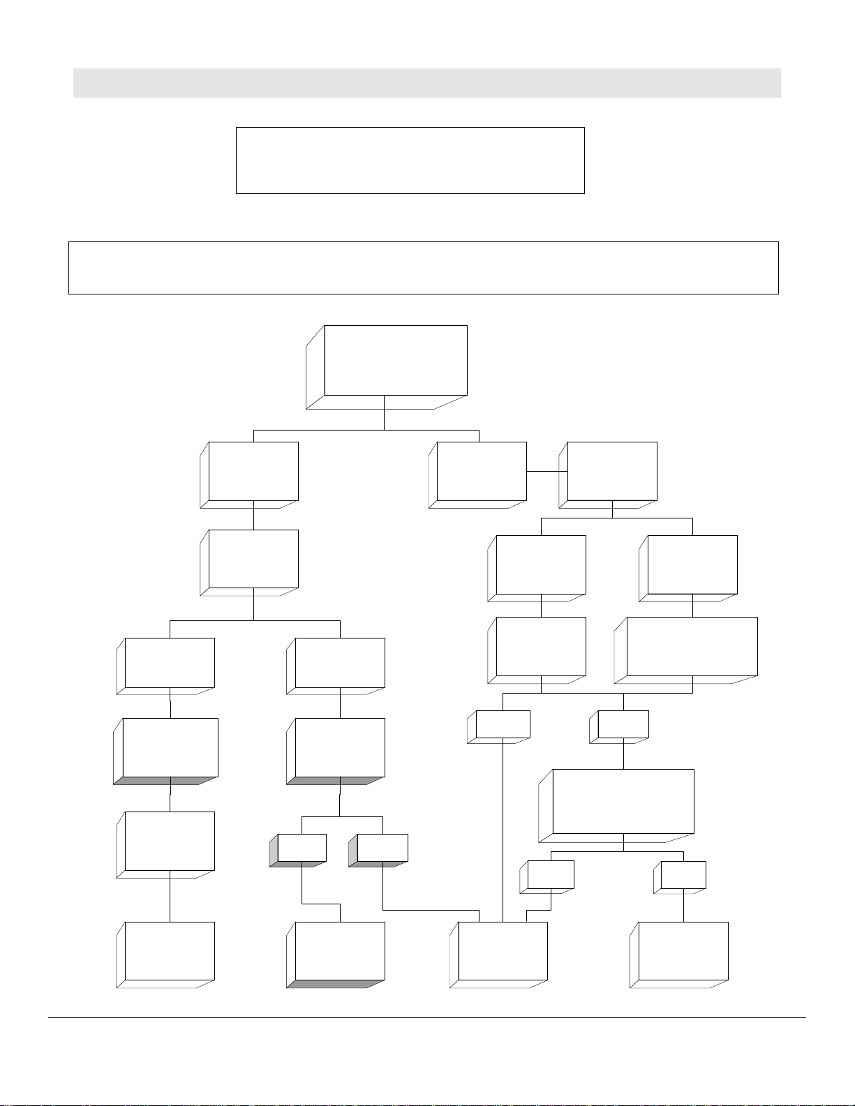
Caution !
V19 / V21 PWB Level Troubleshooting Guide
Troubleshooting Shut-Down Problems
X-Ray Protect
Prior to the diagnostics of these issues, it is imperative that you disable the CRT's to prevent phosphor damage.
Do so by removing Connector SP, which removes filament voltage, or removing each CRT-PCB.
With CRT's disabled
Check HV Block
for arcing
Check Anode
Caps, Spark
Gaps on PCB-
CRT
Unit Shuts
Down
Is there HV
Arcing evident?
NoYes
Check HV
Block for short
or open
N.G. Good
Unit Now
Operates
N.G.
Check High
Voltage
32 KV
Normal High
Check IC5A02
Check IC5A03
Check FBT Pin 8 (2.8 V)
Check Voltage at Cathode
of D5A57 (18.4 V)
Low
Check IC5A00 - IC5A01
Check all Peripheral
Good
Components
Normal
Check CRT-
Sockets. Check
CRT's
Replace HV
Block
Replace Main
PCB
Replace FBT
3333
Page 8
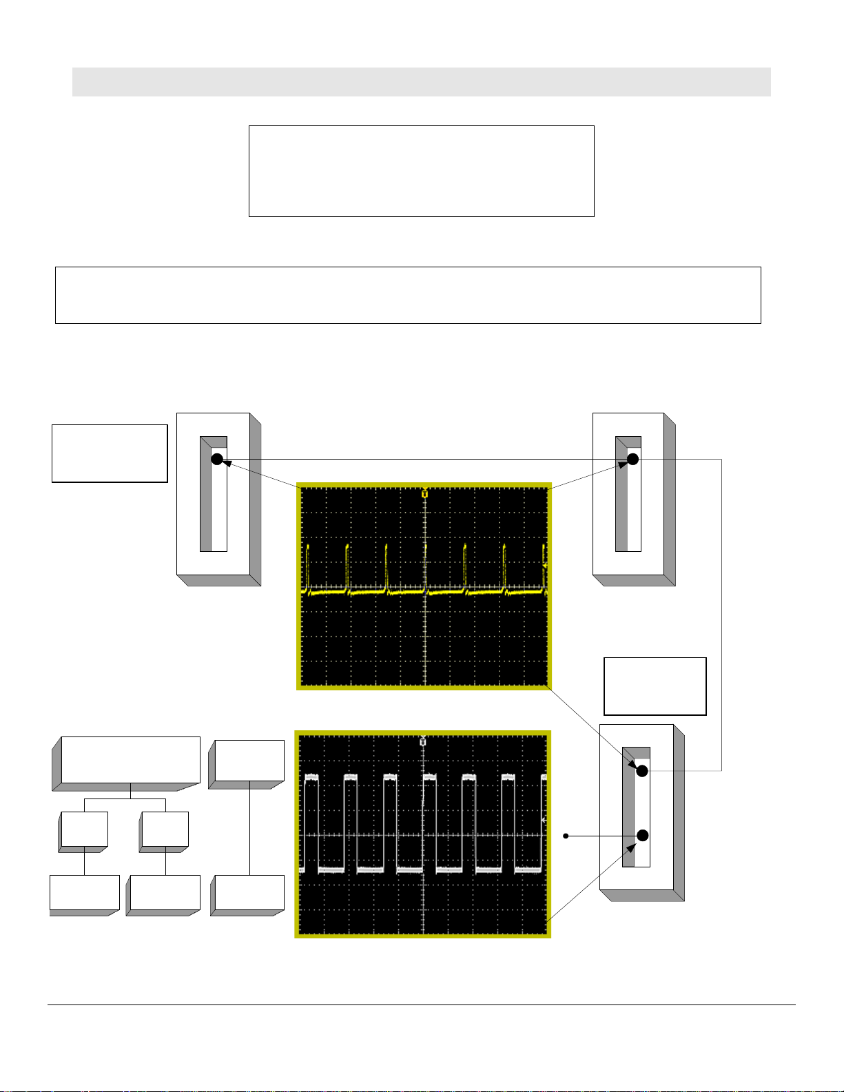
Caution !
V19 / V21 PWB Level Troubleshooting Guide
Troubleshooting Shut-Down Problems
Horizontal Deflection Failure
Do so by removing Connector SP, which removes filament voltage. Also remove D5A13 on the Main PCB to disable the deflection shut-down circuitry
If Missing, Replace
PWB-Signal
Prior to the diagnostics of these issues, it is imperative that you disable the CRT's to prevent phosphor damage.
KE Connector
Pin
17
PWB Signal
Out Out
20 uSec / Div
2.00 V / Div
0.48 V DC
31.5 KHz
4.24 V Pk-Pk
KH Connector
In
Pin
3
PWB Main
If Missing, Replace
PWB-Main
If waveform is missing,
check pin 2 of FB connector
(PWB-Jungle)
Normal
4.4 V
Replace
PWB-Jungle
Low
Replace
PWB-Signal
Waveform
Good
Replace
PWB-Main
20 uSec / Div
2.00 V / Div
4444
31.5 KHz
7.96 V Pk-Pk
3.6 V
DQ Connector
Pin
5
Pin
Out
PWB Jungle
In
3
Page 9

Caution !
V19 / V21 PWB Level Troubleshooting Guide
Troubleshooting Shut-Down Problems
Vertical Deflection Failure
Do so by removing Connector SP, which removes filament voltage. Also remove D5A13 on the Main PCB to disable the deflection shut-down circuitry
If Missing, Replace
PWB-Signal
Prior to the diagnostics of these issues, it is imperative that you disable the CRT's to prevent phosphor damage.
KE Connector
Pin
18
PWB Signal
Out Out
10 mSec / Div
20 uSec / Div
2.00 V / Div
2.00 V / Div
0.46 V DC
31.5 KHz
59.95 Hz
4.24 V Pk-Pk
4.12 V Pk-Pk
KH Connector
In
PWB Main
If Missing, Replace
PWB-Main
Pin
2
If waveform is missing,
check pin 2 of FB connector
(PWB-Jungle)
Normal
4.4 V
Replace
PWB-Jungle
Low
Replace
PWB-Signal
Waveform
Good
Replace
PWB-Main
4 mSec / Div
20 uSec / Div
200 mV / Div
2.00 V / Div
DR Connector
Pin
2
3.6 V
Out
PWB Jungle
59.95 Hz
31.5 KHz
772 mV Pk-Pk
7.96 V Pk-Pk
5555
In
Pin
6
Page 10

V19 / V21 PWB Level Troubleshooting Guide
TV Microprocessor
Diagnostics
IC7A00
Pin 82
Power Good/ Line
0 V
Pin 99
AVCC
5 V
Pin 5
VCC
Pin 1
Reset
5 V
WatchDog IC
5 V
IC7A02
Pin 2
Gnd
Pin 73
Watch Dog Sense
Pulse Waveform
80
Pin 62
5V Stby.
IC7A00
130
Pin 12
Reset
5V
Pin 4
WatchDog Input Data
Pulse Waveform
Pin 3
Master Reset
5 V
Pin 60 & 61
EEPROM Data & Clock
Pin 16
5V Stby.
4.4 V
Pin 46
Short Sense Line
Pin 20
AC-Off
Pin 13 & 15
10 MHz.Xtal Osc.
2.7 V
Waveform
Page 21
Pin 1
12 V Input
5 V
5 V
50
5 V
Regulator
IC9C00
Pin 2
Gnd
Pin 47
X-Ray Sense Line
5 V
Pin 40 & 41
Stby Clock
and Data
4.4 V
Pin 3
5 V Output
Check the following for a No Start Condition
1) Check 5V Supplies to IC on Pins 16, 62, and 99.
All 5V Supplies are sourced from IC9C00, Pin 3
2) Check Reset Pin 12
3) Check for Oscillator operation on Pins 13 and 15
4) Check AC-Off on pin 20, should be High.
5) Check Power Good line Pin 82. Should be Low.
6) Check clock and data signals, Pins 40, 41, 60, and 61.
7) Check for presence of WatchDog pulse on Pin73
Check the following for a Shut-down Condition
1) Check Pin 47, X-Ray Sense line.
This monitors high voltage and Arc-Protection on
the Main PWB. If there is a defect here, go to
deflection troubleshooting procedures.
2) Check Pin 46, Short-Sense line.
This monitors the + /- 24 supplies from the main
power supply, in addition to a 12 V standby supply.
If there is a defect here, go to the power supply
troubleshooting procedures.
6666
Page 11

V19 / V21 PWB Level Troubleshooting Guide
Verify
DC Voltages
and Waveforms prior
to PCB replacement
All Inputs
2HDW
Test
Input a 480P signal to a
component input.
Switch screen Format
between "Standard" and
"Narrow".
PCB
Defect in Color or Video
PCB
2HDW
3DYC
Which Video
Source Input
Shows a defect?
Component PIP Tuner Input 1-5
3DYC
Test
Input Tuner A and
Input 1 NTSC 480i
signal source. Invoke
PIP. Compare Main
picture to PIP Picture
Compare ANT-DTV or
IEEE-1394 input to
any other source
Page 4
Page 3
ANT-DTV
IEEE-1394
DM
Test
Both formats N.G.,
Perform DM Test
If DM signal source is
Defective Signal
good,
Standard Format Good,
Defective 2HDW PCB
Standard Format N.G.
Defective Signal PCB
PCB
Narrow Format N.G.
Narrow Format Good
Main Good
PIP N.G.
Perform 2HDW test
Using 480i source
Main picture N.G.
PIP Good
Defective 3DYC PCB
Main Picture N.G.
PIP Picture N.G.
Perform 2HDW Test
7777
DM Source Good
Other Source N.G.
Perform 2HDW test
DM Picture N.G.
Other Source Good
Defective DM
Both Sources N.G.
Defective Signal PCB
or CRT Drive
Page 12

V19 / V21 PWB Level Troubleshooting Guide
Power Supply
Quick Reference
Power-Pcb Signal-PCB
IC9A20
5
4
3
2
1
IC9A50
5
4
3
2
1
StandBy Supplies
Start-up
Resistor
0.7v
R9A22
16.0V
Ground
0V
163 V
Waveform Page
to PCB-Signal
24V
FA
2
Connector
110V
5KAConnector
Note; 12 V Switched, + / - 24 V Supplies are monitored
by the "Short Sense" line to the TV Microprocessor pin 46
T9A20
21
Off-Board Connectors
to SVM-PCB
D9A33
to CRT-PCB's
220V
12V
Connector
13
12V
1
Connector
D9A30
12 Vs
6Vs
PM
KK
Ref 4V
Switched Supplies
Ground
16.9V
163 V
0V
0.7V
Start-up
Resistor
R9A50
Waveform Page
Refer to Page 1, Printed Circuit Board Diagram, for component and connector locations
21
T9A50
8888
12 Stby
6V in
Q9A22
IC9A22
5
2
D9A57
D9A58
D9A56
D9A60
D9A61
Q9A20
3
1
4
C 36.0V
B 32.6V
E 32.0Vs
220V
110V
19V
24V
-24V
12V Switched
P-on2
Timer Recording
Voltages
Out 5V
D9A35
28 Vs
PF Connector
1
3
4
5
6
7
8
9
10
11
Power-PCB
Gnd
Gnd
Gnd
Gnd
Gnd
12Vs
12Vs
12Vs
12Vs
28Vs
DM
KC Connector
KF Connector
Power-PCB
Gnd
1
Gnd
2
Gnd
3
Gnd
4
Gnd
5
Gnd
6
Gnd
7
6Vs
8
6Vs
9
10
5V
5V
11
12V
12
12V
13
12V
14
12Vs
15
12Vs
16
32Vs
17
P-on2
18
P-on1
19
1
2
3
4
12Vs
5
6
24V
7
8
24V
Gnd
9
10
Gnd
11
Gnd
Gnd
12
Gnd
13
Gnd
14
15
16
110V
17
110V
18
110V
19
Main-PCB
Page 13

V19 / V21 PWB Level Troubleshooting Guide
Main-PCB
Jungle-PCB
Quick Reference
Power-PCB
KH Connector
1
2
3
4
5
6
7
8
9
10
11
12
13
14
15
16
17
18
19
Main-PCB
ID In/O ut DC Waveform
G n d - - -
VD Out .46 P age 14
HD Out .48 Page 14
FP In 0 -
G n d - - -
VTIM O ut .26 Page 14
SC P O ut .95 Page 14
AC L Out 2.8 -
N /C - - -
VB lank O ut 0 -
X-Ray In 5.0 -
N /C - - -
N /C - - -
SC L-Stby I/O 4.5 Data
H-Pulse Out .51 Page 14
Gnd5 - - -
V-Pulse Out .26 Page 14
SD A-Stby I/O 4.5 D ata
HV -Adj O ut 2.0 -
Waveform DC In/O ut ID
- - - H-Gnd
Page 14 4.0 Out Side_Pin
Page 15 3.6 Out H_Drive
Page 15 .57 In H_Pulse
Page 15 .47 In HD
- 9.0 Out FH_Status
- 5.13 Out F33k
- - - N/C
- 9.0 In 9Vsb
- 9.0 In 9Vsb
Refer to Page 1, Printed Circuit Board Diagram, for component and connector locations
Jungle-PCB
DQ Connector
10
1
2
3
4
5
6
7
8
9
Main-PCB
9999
Waveform DC In /O ut ID
Page 14 .95 In SCP-2H
Page 14 .45 In VD
Page 14 .26 In V_Timing
Page 14 0 Out V_Saw
- - - V -Gn d
Page 14 3.4 Out VDRV -
N/A N/A N/A VDRV+
- 12.0 In 12Vsb
Data 4.4 I/O SDA 5
Data 4.4 I/O SC L5
Jungle-PCB
Main-PCB
DR Connector
1
2
3
4
5
6
7
8
9
10
Page 14

V19 / V21 PWB Level Troubleshooting Guide
3DYC-PCB
CRT Drive
Quick Reference
Signal-PCB
EF Connector
1
2
3
4
5
6
7
8
9
10
11
12
13
14
15
16
17
18
19
20
21
22
23
24
25
26
27
28
29
30
31
32
33
34
35
3DYC-PCB
ID In /O ut DC Waveform
Gn d - - -
3D_Hsync In .58 Page 15
Gn d - - -
3D_Vsync In .15 Page 15
M _F run - - -
3D_Csync In 4.7 Page 15
NT_Sw In - -
3D_Pb Out 3.0 Page 15
Gn d - - -
3D_Pr Out 3.0 P age 15
Gn d - - -
3D-Y Out 2.8 P age 15
Gn d - - -
SDA-3D I/O 4.4 Data
SCL-3D I/O 4.4 Data
9V-1 In 9.0 -
9V-1 In 9.0 -
Kil In 0 -
3DRst In 5.0 -
5V In 5.0 -
5V In 5.0 -
Gn d - - -
Gn d - - -
VY_3D YC In 3.76 Page 15
Gn d - - -
C_3DY C In 2.62 Page 15
Gn d - - -
Gn d - - -
Gn d - - -
Y-Mon O ut 2.62 Page 15
Gn d - - -
C-Mon O ut 2.6 P age 16
Gn d - - -
Gn d - - -
Gn d - - -
CRT-PCB's
Signal-PCB
RM Connector
1
3
4
5
6
7
8
CRT Drive
Signal-PCB
ID In/Ou t DC Waveform
R_Out Out 2.9 Page 16
- - - -
Gnd - - -
G_Out Out 3.13 Page 16
Gnd - - -
B_Out Out 2.9 Page 16
Gnd - - -
Ik In 2.0 Page 16
Refer to Page 1, Printed Circuit Board Diagram, for component and connector locations
10
10
1010
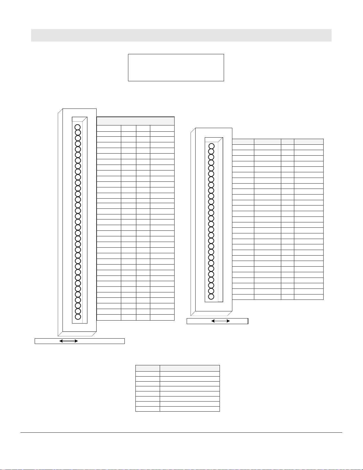
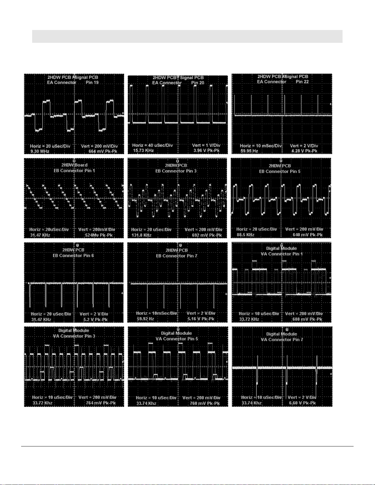
Page 15

EA Connector
1
2
3
4
5
6
7
8
9
10
11
12
13
14
15
16
17
18
19
20
21
22
Signal-PCB
2HDW (Line Doubler) PCB
Quick Reference
ID In/O u t DC Waveform
PIP-Y In 3.0 Page 16
Gnd - - -
PIP-PB In 2.85 Page 16
Gnd - - -
PIP-PR In 2.83 Page 16
PIP-H In .58 Page 16
Gnd - - -
PIP-V In .16 Page 16
3.3V In 3.3 -
3.3V In 3.3 -
Gnd - - -
Gnd - - -
9V-2 In 9.0 -
Gnd - - -
AMDP-Y-In In 2.36 Page 16
Gnd - - -
AMDP-PB-In In 2.2 Page 16
Gnd - - -
AMD-PR-In In 2.2 Page 17
Main-H In .58 Page 17
Gnd - - -
Main-V In .15 Page 17
Waveform DC In/Out ID
2HDW-PCB
Page 17 2.25 Out Y-AMDP
- - Gnd
Page 17 2.65 Out PB-AMDP
- - Gnd
Page 17 2.65 Out PR-AMDP
Page 17 4.5 Out H-AMDP
Page 17 4.8 Out V-AMDP
- - - G nd
- - Out YS-AMDP
- - - G nd
- - Out FP
- - - N /C
- - In 5 V- A
- - In 5V
- - - G nd
Data 3.8 I/O SDA-AMDP
Data 3.8 I/O SCL-AMDP
- - - G nd
Data .18 I/O CS-AMDP
Data 5.0 I/O Clk
Data 3.18 In D _In
Data 5.0 Out D_Out
V19 / V21 PWB Level Troubleshooting Guide
2HDW-PCB
EB Connector
Signal-PCB
1
2
3
4
5
6
7
8
9
10
11
12
13
14
15
16
17
18
19
20
21
22
Refer to Page 1, Printed Circuit Board Diagram, for component and connector locations
11
11
1111
Page 16

V19 / V21 PWB Level Troubleshooting Guide
Digital Module
Quick Reference
Signal-PCB
Signal-PCB
DM Assembly
VA Connector
1
2
3
4
5
6
7
8
9
10
11
12
13
DA Connector
1
2
3
4
5
6
7
8
9
10
11
12
13
14
ID In/Out DC Waveform
DM-G Out 2.4 Page 17
Gnd - - -
DM-B Out 2.4 Page 17
Gnd - - -
DM-R Out 2.4 Page 17
Gnd - - -
DM-H Out 3 .11 Page 17
DM-V Out 3 .22 Page 18
Gnd - - -
DSP-H In .44 Page 18
DSP-V In 0 Page 18
Gnd - - -
Masking Out 0 High = OSD on
DM Assembly
ID
L-DM Out HD Audio
Gnd - - -
R-DM Out HD Audio
Gnd - - -
DM _Reset In 0V -
Powergood Out 0V
TV-DM_RTS I/O Data
TV-DM_CTS I/O Data
DM_Rxd I/O Data
Gnd - - -
TV-DM_Txd I/O Data
DMDetect Out 0V
IR_In_Busy Out Data
IR_Out_ENA In Data
In/Ou t DC Waveform
DM Assembly
Waveform DC In/O ut ID
Page 1 8 .9 In Ma in -Y
- - - G nd
Page 18 2.2 In M ain-CB
- - - G nd
Page 18 2.2 In M ain-CR
- - - G nd
Page 18 4.7 In Main_Sync
- - - N /C
- - - G nd
- 5.0 Out TV_Reset
- - - G nd
Page* 18 .9* Out Y-DM
- - - G nd
Page* 18 .9* O ut C-DM
- - - G nd
* Available in HDTV or
OSD Modes Only
DM Assembly
Power-PCB
PF Connector
Gnd
1
3
Gnd
4
Gnd
Gnd
5
Gnd
6
12Vs
12Vs
12Vs
12Vs
32Vs
7
8
9
10
11
Signal-PCB
DB Connector
1
2
3
4
5
6
7
8
9
10
11
12
13
14
15
Voltages and Waveforms taken in 480i mode except where indicated
Refer to Page 1, Printed Circuit Board Diagram, for component and connector locations
12
12
1212
Page 17
Convergence Generator
VD Connector
1
2
3
4
5
6
7
8
9
10
11
12
13
14
15
16
17
18
19
20
21
22
23
24
25
26
27
28
29
30
31
32
33
34
35
C_E2Reset In 5.0 -
C_Mute In 5.0 -
C-Reset In 5.0 -
C_Busy I/O 4.5 -
HPulse In .56 Page 18
HV-Adj In 1.8 -
VPulse In .25 Page 18
C_OSDr Out 0 -
C_OSDg Out 0 -
C_OSDb Out 0 -
Convergence
Quick Reference
ID In /
N/C - - -
12V In 12.0 -
C_Ack I/O 4.8 -
C-Sda I/O 4.2 Data
C_Scl I/O 4.2 Data
N/C - - -
Gn d - - Gn d - - -
N/C - - -
N/C - - -
C_Blk Out - -
5V In 5.0 -
N/C - - -
Gn d - - -
Gn d - - -
Gn d - - -
9V In 9.0V -
DF Out -1.7 Page 18
-9V In -9 .0 -
BV O ut .12 Pag e 19
GV Out 0 Page 19
RV Out 0 Page 19
BH O ut .5 Page 1 9
GH O ut .14 Pag e 19
RH O ut .15 Pag e 19
Out
DC Waveform
V19 / V21 PWB Level Troubleshooting Guide
Convergence IC
IC8C01
1
2
3
4
5
6
7
8
9
10
11
12
13
14
15
16
17
18
19
20
21
22
23
24
25
26
27
28
Power-PCB
ID In / Ou t DC Waveform
BH In .257 Page 19
-BH Yoke Return .257 Page 19
+BH Out .45 Page 19
+GH Out .20 P age 19
-GH Yoke Return 0 Page 19
GH In 0 Page 19
RH In .28 Page 20
_RH Yoke Return .28 Page 20
+RH Out 0 Page 20
-VCC In -24 -
N/C - - -
VCC In 24 -
Pre+VCC In 24 -
Gnd - - -
Pre-VCC In -24 -
-VCC2 In -24 -
Gnd - - -
Vcc2 In 24 -
Mute In 5.0 -
+RV Out 0 Page 20
-RV Yoke Return 0 Page 20
RV In 0 Page 20
GV In 0 Page 20
-GV Yoke Return .1 Page 20
+GV Out 0 Page 20
+BV Out .1 Page 21
-BV Yoke Return .2 Page 21
BV In .2 Page 21
IC8C01
Power-PCB
Convergence Generator
Partial Glossary
ID Definition
C_E2Reset Reset Pulse from EEPROM
C_Ack Convergence Acknowledge
C_SDA Conver gence Serial Data
C_SCL Convergence Serial Clock
HPulse Horizontal Pulse
VPulse Vertical Pulse
C_OSD Convergence On Screen Display
DF Dynamic B eam Forming Pulse
Refer to Page 1, Printed Circuit Board Diagram, for component and connector locations
13
13
1313
Page 18

V19 / V21 PWB Level Troubleshooting Guide
14
14
1414
Page 19

V19 / V21 PWB Level Troubleshooting Guide
15
15
1515
Page 20

V19 / V21 PWB Level Troubleshooting Guide
16
16
1616
Page 21
V19 / V21 PWB Level Troubleshooting Guide
17
17
1717
Page 22

V19 / V21 PWB Level Troubleshooting Guide
18
18
1818
Page 23

V19 / V21 PWB Level Troubleshooting Guide
19
19
1919
Page 24

V19 / V21 PWB Level Troubleshooting Guide
20
19
1919
Page 25

V19 / V21 PWB Level Troubleshooting Guide
 Loading...