

Page 1
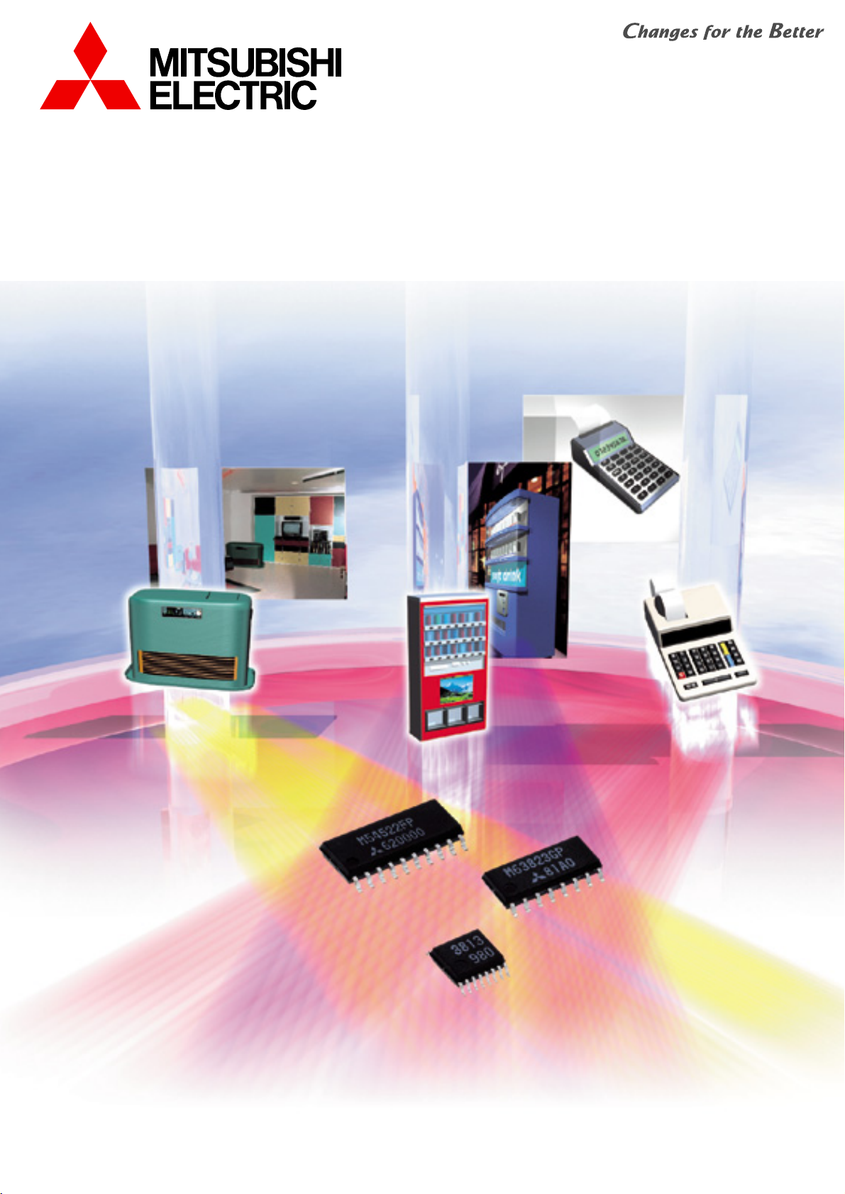
Transistor-Array series
Transistor-Array series
Wide products range help reduce applications sets size and weight
Page 2
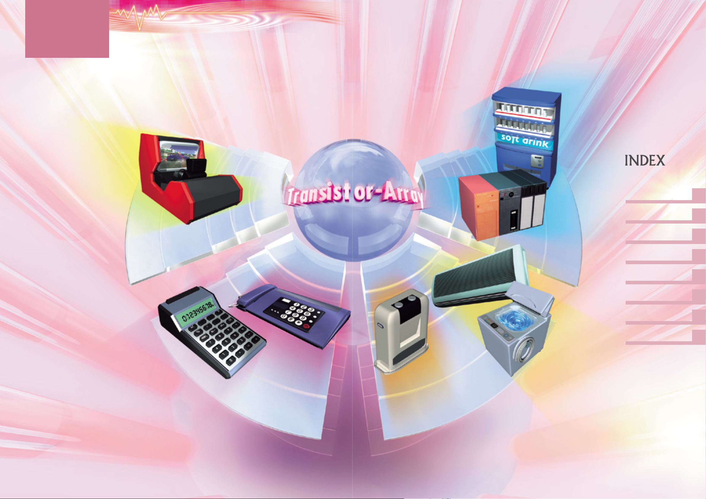
●
Vending machines
●
Sequencers
●
Measurement instruments
●
Elevators
●
Air-conditioner
●
Fan heater
●
Washing machine
●
Refrigerator
●
Hot water dispenser
Function reference.
Codes for transistor array type name
Application reference
Quick reference
Circuit/Pin connection
Thermal derating
factor characteristics
P3
P4
P5
P7
P14
How to use
P15
Application examples
P17
Package outlines
P21
H
o
m
e
e
l
e
c
t
r
o
n
i
c
s
I
n
d
u
s
t
r
i
a
l
e
q
u
i
p
m
e
n
t
2
●
Arcade games
●
Slot machine
●
Copy machine
●
FAX
●
Printer
●
Calculator with printer
Transistor Array is a semiconductor integrated circuit in which a minute input
current enables a high current drive. Transistor Arrays are used in a wide
range of fields therefore they are available in an abundant product series
(
30mA to 1.5A/20V to 80V).
Utilization of surface-mount packages also enables compact, lightweight, and
high density mounting of the target applications sets.
A
m
u
s
e
m
e
n
t
O
f
f
i
c
e
a
u
t
o
m
a
t
i
o
n
e
q
u
i
p
m
e
n
t
1
Application
Page 3
Function reference
Output withstand voltage
High withstand
voltage
(50V MIN.)
High withstand
voltage
(50V MIN.)
3V line
Low withstand
voltage
(50V less than)
Collector current Output format Input active level Type name
M54523P/FP
M54525AGP
M54526P/FP
M54532P/FP
M54585P/FP/KP
M54666P
M63823P/FP/GP
M63826P/FP/GP
M54567P/FP
M54587P/FP
M54661P/FP
M54562P/FP
M54563P/FP
M54564P/FP
M63800FP
M54667P
M54566P/FP
M54583P/FP
M54580P/FP
M63820FP/KP
M63824GP/KP
M63830P/FP
M63832GP/KP
M63834FP/KP
M63836FP/KP
M54516P
M54539P
M54513P/FP
M54514AP/AFP
M54517P
M54519P/FP
M54522P/FP
M54527P
M54528P
M54530P/FP
M54531P/FP
M54534P/FP
M54537P/FP
M54571P
M54577P
M63802P/FP/GP/KP
M63803P/FP/GP/KP
M63804P/FP/GP/KP
M63805P/FP/KP
M63806P/FP/KP
M63807P/FP/KP
M63812P/FP/GP/KP
M63813P/FP/GP/KP
M63814P/FP/GP/KP
M63815P/FP/KP
M63816P/FP/KP
M63817P/FP/KP
M54560P
M54561P
:
쏒쏒
Under development
500mA MIN.
500mA less than
500mA MIN.
500mA MIN.
500mA less than
Sink
Source
Sink
Source
Sink
Sink
Sink
Source
"H"
"L"
"H"
"L"
"L"
"L"
"H"
"L"
"H"
"H"
"L"
★★
★★
★★
★★
★★
★★
Codes for transistor array type name
M
5
M
M
M
4523
5
4525
6
3802
6
3823
3
P
GP
A
KP
FP
Package type
.....
P:DIP type FP/GP:SOP type KP:SSOP type
Auxiliary signal
Circuit type and circuit kind per product's series
Application and the range of ambient temperature for operation
Abbreviation shows the Mitsubishi Integrated Circuit
Page 4
2000
1500
1000
700
500
300
200
150
100
70
50
30
20
10
0
10 20 30 40 50 60 70 80 90 100
Output voltage[V]
Output current [mA]
Lamp
Relay
Wire dot and daisy head
Mini printer head
M54516
쏹
Plunger
쏹
M54580
Fluorescent
LED
쏹
쏹
쏹
쏹
쏹
쏹
M54667
M54517
쏹
Thermal head
M54537
쏹
M54534
쏹
쏹
쏹
M54571
쏹
M54561
쏹
쏹
M54514A
쏹
M54513
M54519
M54522
M54530
M54531
M63820
M63824
M63832
M63834
M63836
쏒쏒
쏒쏒
쏒쏒
쏒쏒
쏒쏒
M63830
쏒쏒
M54527
M54528
M54560
M63802
M63803
M63804
M63805
M63806
M63807
M63812
M63813
M63814
M63815
M63816
M63817
M54523
M54525A
M54526
M54562
M54563
M54564
M54585
M54587
M63800
M63823
M63826
M54566
M54583
M54532
M54567
M54661
M54666
M54577
쏹
4
Application reference
쏒쏒
:
Under development
3V line
3V line
Page 5
Quick reference
5
:
Recommended product
Type name
Package
outlines
Unit
LED
Input-
function
voltage
Low input
voltage
operation
Output
current
Io max
[mA]
Vo max
(V)
Darlington
transistor
With output
clamp
diode
Low VCE
(sat)
Input
diode
Mini-frat
package
Solenoid Relay
Features
Lamp
Application
1
2
3
4
5
6
7
8
9
10
11
12
13
14
15
16
17
18
19
20
21
22
23
24
25
26
27
28
29
30
31
32
33
34
35
36
37
38
39
40
41
42
43
44
45
46
47
48
49
50
51
52
53
54
55
56
57
58
M54513P
M54513FP
M54514AP
M54514AFP
M54516P
M54517P
M54519P
M54519FP
M54522P
M54522FP
M54523P
M54523FP
M54525AGP
M54526P
M54526FP
M54527P
M54528P
M54530P
M54530FP
M54531P
M54531FP
M54532P
M54532FP
M54534P
M54534FP
M54537P
M54537FP
M54539P
M54560P
M54561P
M54562P
M54562FP
M54563P
M54563FP
M54564P
M54564FP
M54566P
M54566FP
M54567P
M54567FP
M54571P
M54577P
M54580P
M54580FP
M54583P
M54583FP
M54585P
M54585FP
M54585KP
M54587P
M54587FP
M54661P
M54661FP
M54666P
M54667P
M63800FP
M63802P
M63802FP
18P4G
20P2N
16P4
16P2N
14P4
16P4
16P4
16P2N
18P4G
20P2N
16P4
16P2N
16P2S
16P4
16P2N
14P4
16P4
16P4
16P2N
16P4
16P2N
16P4
16P2N
16P4
16P2N
16P4
16P2N
16P4
16P4
16P4
18P4G
20P2N
18P4G
20P2N
18P4G
20P2N
16P4
16P2N
16P4
16P2N
20P4
16P4
16P4
16P2N
18P4G
20P2N
18P4G
20P2N
20P2E
20P4
20P2N
16P4
16P2N
16P4
20P4
16P2N
16P4
16P2N
쎻
쎻
쎻
쎻
쎻
쎻
쎻
쎻
쎻
쎻
쎻
쎻
쎻
쎻
쎻
쎻
쎻
쎻
쎻
쎻
쎻
쎻
쎻
쎻
쎻
쎻
쎻
쎻
쎻
쎻
쎻
쎻
쎻
쎻
쎻
쎻
쎻
쎻
쎻
쎻
쎻
쎻
쎻
쎻
쎻
쎻
쎻
쎻
쎻
쎻
쎻
쎻
쎻
쎻
쎻
쎻
쎻
쎻
쎻
쎻
쎻
쎻
쎻
쎻
쎻
쎻
쎻
쎻
쎻
쎻
쎻
쎻
쎻
쎻
쎻
쎻
쎻
쎻
쎻
쎻
쎻
쎻
쎻
쎻
쎻
쎻
쎻
쎻
쎻
쎻
쎻
쎻
쎻
쎻
쎻
쎻
쎻
쎻
쎻
쎻
쎻
쎻
쎻
쎻
쎻
쎻
쎻
쎻
쎻
쎻
쎻
쎻
쎻
쎻
쎻
쎻
쎻
쎻
쎻
쎻
쎻
쎻
쎻
쎻
쎻
쎻
쎻
쎻
쎻
쎻
쎻
쎻
쎻
쎻
쎻
쎻
쎻
쎻
쎻
쎻
쎻
쎻
쎻
쎻
쎻
쎻
쎻
쎻
쎻
쎻
쎻
쎻
쎻
쎻
쎻
쎻
쎻
쎻
쎻
쎻
쎻
쎻
쎻
쎻
쎻
쎻
H
H
H
H
H
H
H
H
H
H
H
H
H
H
H
H
H
H
H
H
H
H
H
H
H
H
H
H
L
L
H
H
H
H
H
H
L
L
L
L
H
H
L
L
L
L
H
H
H
L
L
L
L
L
H
L
H
H
Sink
Sink
Sink
Sink
Sink
Sink
Sink
Sink
Sink
Sink
Sink
Sink
Sink
Sink
Sink
Sink
Sink
Sink
Sink
Sink
Sink
Sink
Sink
Sink
Sink
Sink
Sink
Sink
Source
Source
Source
Source
Source
Source
Source
Source
Sink
Sink
Sink
Sink
Sink
Sink
Source
Source
Sink
Sink
Sink
Sink
Sink
Sink
Sink
Sink
Sink
Sink
Source
Source
Sink
Sink
50
50
50
50
500
400
400
400
400
400
500
500
500
500
500
150
150
400
400
400
400
1500
1500
320
320
350
350
700
150
300
500
500
500
500
500
500
400
400
1500
1500
350
30
150
150
400
400
500
500
500
500
500
1500
1500
1500
500
500
300
300
40
40
20
20
25
25
40
40
40
40
50
50
50
50
50
40
40
40
40
40
40
50
50
20
20
20
20
20
40
40
50
50
50
50
50
50
50
50
50
50
40
30
50
50
50
50
50
50
50
50
50
80
80
80
80
50
35
35
쎻
쎻
쎻
쎻
쎻
쎻
쎻
쎻
쎻
쎻
쎻
쎻
쎻
쎻
쎻
쎻
쎻
쎻
쎻
쎻
쎻
쎻
쎻
쎻
쎻
쎻
쎻
쎻
쎻
쎻
쎻
쎻
쎻
쎻
쎻
쎻
쎻
쎻
쎻
쎻
쎻
쎻
쎻
쎻
쎻
쎻
쎻
쎻
쎻
쎻
쎻
쎻
쎻
쎻
쎻
쎻
쎻
쎻
쎻
쎻
쎻
쎻
쎻
쎻
쎻
쎻
쎻
쎻
쎻
쎻
쎻
쎻
쎻
쎻
쎻
쎻
쎻
쎻
쎻
쎻
쎻
쎻
쎻
쎻
쎻
쎻
쎻
쎻
쎻
쎻
쎻
쎻
쎻
쎻
쎻
쎻
쎻
쎻
쎻
쎻
쎻
쎻
쎻
쎻
쎻
쎻
쎻
쎻
쎻
쎻
쎻
쎻
쎻
쎻
쎻
쎻
쎻
쎻
쎻
쎻
쎻
쎻
쎻
쎻
쎻
쎻
쎻
쎻
쎻
쎻
쎻
쎻
쎻
쎻
쎻
쎻
쎻
쎻
쎻
쎻
쎻
쎻
쎻
쎻
쎻
쎻
쎻
쎻
쎻
쎻
쎻
쎻
쎻
쎻
쎻
쎻
쎻
쎻
쎻
쎻
쎻
쎻
쎻
쎻
쎻
쎻
쎻
쎻
쎻
쎻
쎻
쎻
쎻
쎻
쎻
쎻
쎻
쎻
쎻
쎻
쎻
쎻
쎻
쎻
쎻
쎻
8
8
7
7
5
7
7
7
8
8
7
7
7
7
7
6
7
7
7
7
7
4
4
6
6
7
7
6
7
7
8
8
8
8
8
8
7
7
4
4
6
7
7
7
8
8
8
8
8
8
8
4
4
4
8
7
7
7
Page 6

6
:
Recommended product
쏒쏒
:
Under development
Type name
Package
outlines
Unit
LED
Input-
function
voltage
Output
current
Io max
[mA]
Vo max
(V)
Darlington
transistor
With output
clamp
diode
Mini-frat
package
Solenoid Relay
Application Features
Lamp
Low input
voltage
operation
Low VCE
(sat)
Input
diode
M63802GP
M63802KP
M63803P
M63803FP
M63803GP
M63803KP
M63804P
M63804FP
M63804GP
M63804KP
M63805P
M63805FP
M63805KP
M63806P
M63806FP
M63806KP
M63807P
M63807FP
M63807KP
M63812P
M63812FP
M63812GP
M63812KP
M63813P
M63813FP
M63813GP
M63813KP
M63814P
M63814FP
M63814GP
M63814KP
M63815P
M63815FP
M63815KP
M63816P
M63816FP
M63816KP
M63817P
M63817FP
M63817KP
M63820FP
M63820KP
M63823P
M63823FP
M63823GP
M63824GP
M63824KP
M63826P
M63826FP
M63826GP
M63830P
M63830FP
M63832GP
M63832KP
M63834FP
M63834KP
M63836FP
M63836KP
16P2S
16P2Z
16P4
16P2N
16P2S
16P2Z
16P4
16P2N
16P2S
16P2Z
18P4G
20P2N
20P2E
18P4G
20P2N
20P2E
18P4G
20P2N
20P2E
16P4
16P2N
16P2S
16P2Z
16P4
16P2N
16P2S
16P2Z
16P4
16P2N
16P2S
16P2Z
18P4G
20P2N
20P2E
18P4G
20P2N
20P2E
18P4G
20P2N
20P2E
20P2N
20P2E
16P4
16P2N
16P2S
16P2S
16P2Z
16P4
16P2N
16P2S
16P4
16P2N
16P2S
16P2Z
20P2N
20P2E
20P2N
20P2E
7
7
7
7
7
7
7
7
7
7
8
8
8
8
8
8
8
8
8
7
7
7
7
7
7
7
7
7
7
7
7
8
8
8
8
8
8
8
8
8
8
8
7
7
7
7
7
7
7
7
4
4
7
7
8
8
8
8
쎻
쎻
쎻
쎻
쎻
쎻
쎻
쎻
쎻
쎻
쎻
쎻
쎻
쎻
쎻
쎻
쎻
쎻
쎻
쎻
쎻
쎻
쎻
쎻
쎻
쎻
쎻
쎻
쎻
쎻
쎻
쎻
쎻
쎻
쎻
쎻
쎻
쎻
쎻
쎻
쎻
쎻
쎻
쎻
쎻
쎻
쎻
쎻
쎻
쎻
쎻
쎻
쎻
쎻
쎻
쎻
쎻
쎻
쎻
쎻
쎻
쎻
쎻
쎻
쎻
쎻
쎻
쎻
쎻
쎻
쎻
쎻
쎻
쎻
쎻
쎻
쎻
쎻
쎻
쎻
쎻
쎻
쎻
쎻
쎻
쎻
쎻
쎻
쎻
쎻
쎻
쎻
쎻
쎻
쎻
쎻
쎻
쎻
쎻
쎻
쎻
쎻
쎻
쎻
쎻
쎻
쎻
쎻
쎻
쎻
쎻
쎻
쎻
쎻
쎻
쎻
쎻
쎻
쎻
쎻
쎻
쎻
쎻
쎻
쎻
쎻
쎻
쎻
쎻
쎻
쎻
쎻
쎻
쎻
쎻
쎻
쎻
쎻
쎻
쎻
쎻
쎻
쎻
쎻
쎻
쎻
쎻
쎻
쎻
쎻
쎻
쎻
쎻
쎻
쎻
쎻
쎻
쎻
쎻
쎻
쎻
쎻
쎻
쎻
쎻
쎻
쎻
쎻
쎻
쎻
쎻
쎻
쎻
쎻
H
H
H
H
H
H
H
H
H
H
H
H
H
H
H
H
H
H
H
H
H
H
H
H
H
H
H
H
H
H
H
H
H
H
H
H
H
H
H
H
H
H
H
H
H
H
H
H
H
H
L
L
L
L
L
L
L
L
Sink
Sink
Sink
Sink
Sink
Sink
Sink
Sink
Sink
Sink
Sink
Sink
Sink
Sink
Sink
Sink
Sink
Sink
Sink
Sink
Sink
Sink
Sink
Sink
Sink
Sink
Sink
Sink
Sink
Sink
Sink
Sink
Sink
Sink
Sink
Sink
Sink
Sink
Sink
Sink
Sink
Sink
Sink
Sink
Sink
Sink
Sink
Sink
Sink
Sink
Sink
Sink
Sink
Sink
Sink
Sink
Sink
Sink
300
300
300
300
300
300
300
300
300
300
300
300
300
300
300
300
300
300
300
300
300
300
300
300
300
300
300
300
300
300
300
300
300
300
300
300
300
300
300
300
500
500
500
500
500
500
500
500
500
500
1500
1500
500
500
500
500
500
500
35
35
35
35
35
35
35
35
35
35
35
35
35
35
35
35
35
35
35
35
35
35
35
35
35
35
35
35
35
35
35
35
35
35
35
35
35
35
35
35
50
50
50
50
50
50
50
50
50
50
50
50
50
50
50
50
50
50
쎻
쎻
쎻
쎻
쎻
쎻
쎻
쎻
쎻
쎻
쎻
쎻
쎻
쎻
쎻
쎻
쎻
쎻
쎻
쎻
쎻
쎻
쎻
쎻
쎻
쎻
쎻
쎻
쎻
쎻
쎻
쎻
쎻
쎻
쎻
쎻
쎻
쎻
쎻
쎻
쎻
쎻
쎻
쎻
쎻
쎻
쎻
쎻
쎻
쎻
쎻
쎻
쎻
쎻
쎻
쎻
쎻
쎻
쎻
쎻
쎻
쎻
쎻
쎻
쎻
쎻
쎻
쎻
쎻
쎻
쎻
쎻
쎻
쎻
쎻
쎻
쎻
쎻
쎻
쎻
쎻
쎻
쎻
쎻
쎻
쎻
쎻
쎻
쎻
쎻
쎻
쎻
쎻
쎻
쎻
쎻
쎻
쎻
쎻
쎻
쎻
쎻
쎻
쎻
쎻
쎻
쎻
쎻
쎻
쎻
쎻
쎻
쎻
쎻
쎻
쎻
쎻
쎻
쎻
쎻
쎻
쎻
쎻
쎻
쎻
쎻
쎻
쎻
쎻
쎻
쎻
쎻
쎻
쎻
쎻
쎻
쎻
쎻
쎻
쎻
쎻
쎻
쎻
쎻
쎻
쎻
쎻
쎻
쎻
쎻
쎻
쎻
쎻
쎻
쎻
쎻
쎻
쎻
쎻
쎻
쎻
쎻
쎻
쎻
쎻
쎻
쎻
쎻
쎻
쎻
쎻
쎻
쎻
쎻
쎻
쎻
쎻
쎻
쎻
쎻
쎻
쎻
쎻
쎻
쎻
쎻
쎻
쎻
쎻
쎻
쎻
쎻
쎻
쎻
쎻
쎻
쎻
쎻
쎻
쎻
쎻
쎻
쎻
쏒쏒
쏒쏒
쏒쏒
쏒쏒
쏒쏒
쏒쏒
쏒쏒
쏒쏒
쏒쏒
쏒쏒
쏒쏒
쏒쏒
59
60
61
62
63
64
65
66
67
68
69
70
71
72
73
74
75
76
77
78
79
80
81
82
83
84
85
86
87
88
89
90
91
92
93
94
95
96
97
98
99
100
101
102
103
104
105
106
107
108
109
110
111
112
113
114
115
116
Page 7
Type name Circuit diagram Pin connection
Package
outlines
Io max.
(mA)
Vo max.
(V)
8
10
NC
GND
12131415 11161718
75432619
9
11
NC NC
NC GND
13141516 12171819
865437220110
NC
910111213141516
GND
86543721
NC
910111213141516
GND
86543721
NC NC
91011121314
GNDNC
8
6543721
8
10
COM
GND
12131415 11161718
75432619
9
11
NC COM
NC GND
13141516 12171819
865437220110
7
NC : No connection
M54513P/FP
4050
M54514AP/AFP
2050
M54516P
25500
M54517P
25400
M54519P/FP
40400
M54522P/FP
40400
18P4G
20P2N
2K
13.6K
IN
OUT
GND
2.8K
10K
IN
OUT
GND
20K
20K
2K
IN
OUT
GND
20K
20K
2K
IN
OUT
COM
GND
16P4
16P2N
14P4
16P4
16P4
16P2N
18P4G
20P2N
Circuit/Pin connection
M54523P/FP
50500
9
COM
10111213141516
8
GND
6543721
2.7K
5K
3K
IN
OUT
COM
GND
16P4
16P2N
Page 8

8
NC : No connection
Type name Circuit diagram Pin connection
Package
outlines
Io max.
(mA)
Vo max.
(V)
M54525AGP
50500
M54526P/FP
50500
M54527P
40150
M54528P
40150
M54530P/FP
40400
M54531P/FP
40400
M54532P/FP
501500
9
COM
10111213141516
8
GND
6543721
10.5K
5K
3K
IN
OUT
COM
GND
10.5K
5K
3K
IN
OUT
COM
Vz=7V
GND
20K
20K
2K
IN
OUT
COM
GND
COM
91011121314
GND
8
6543721
COM
910111213141516
GND
86543721
9
COM
10111213141516
8
GND
6543721
20K
20K
2K
IN
OUT
COM
GND
340
5.5K
3K
IN
OUT
COM
GND
20K
20K
2K
IN
OUT
COM
GND
9
NCGNDNC
10111213141516
8
COMGNDCOM
6543721
16P4
16P2N
16P2S
14P4
16P4
16P4
16P2N
16P4
16P2N
M54534P/FP
20320
16P2N
16P4
9
COM
10111213141516
8
GND
Vcc
STB
6543721
2K
1.6K
380
20K
IN
STB
OUT
COM
Vcc
GND
Page 9

Circuit/Pin connection
Type name Circuit diagram Pin connection
Io max.
(mA)
M54537P/FP
M54539P
M54560P
Vo max.
(V)
20350
20700
40150
380
Vcc
2K
IN
20K
2K
IN
20K
IN
20K
2K
200
2K
27K
7K
OUT
GND
Vcc
COM
OUT
GND
Vs
OUT
SUB
Package
outlines
Vcc
9
10111213141516
16P4
8
6543721
GND
COMVcc
9
10111213141516
8
6543721
GNDNC
SUB
9
10111213141516
16P2N
16P4
M54561P
M54562P/FP
M54563P/FP
27K
IN
40300
50500
50500
20K
8.5K
IN
3K
IN
7K
3K
20K
7.2K
1.5K
20K
7.2K
1.5K
Vs
OUT
SUB
Vs
OUT
3K
GND
Vs
OUT
3K
GND
NC GND
NC Vs
8
6543721
Vs
GND
10
12131415 11161718
8
75432619
Vs
11
13141516 12171819
9
865437220110
GND
10
12131415 11161718
16P4
18P4G
20P2N
9
M54564P/FP
20K
50500
8K
IN
20K
1.5K
7.2K
50K
Vs
8
75432619
Vs
OUT
3K
GND
NC
GND
1113141516 12171819
18P4G
20P2N
9
865437220110
NC
Vs
NC : No connection
Page 10

Type name Circuit diagram Pin connection
Io max.
(mA)
M54566P/FP
M54567P/FP
Vo max.
(V)
50400
501500
20K
IN
8K
IN
22K
8K
2.7K
7.2K
3K
2K
5.5K
3K
Vcc
OUT
OUT
Vcc
COM
OUT
GND
Package
outlines
Vcc
9
10111213141516
16P4
8
6543721
GND
COMGNDCOM
9
10111213141516
8
6543721
VccGNDVcc
16P2N
16P4
16P2N
M54571P
M54577P
M54580P/FP
V
B
7K
50K
22K
150
150
10K
3K
30K
Vcc
OUT
GND
Vs
OUT
GND
4.3K
IN1
30K
V
Vs I
VZ
VS
IDF
GND
2K
20K
40350
23K
3030
50150
IN
100K
30K
IN
7K
OUT1
600
2K
B VZ VP COM
DF NC GND
4.3K
IN6
30K
OUT6
V
P
600
2K
COM
GND
20P4
11
13141516 12171819
9
865437220110
Vcc
9
10111213141516
8
6543721
GND
9Vs10111213141516
16P4
16P4
8
6543721
GND
16P2N
M54583P/FP
Vcc
10
12131415 11161718
7K
50400
IN
2.7K
7K
7.2K
Vcc
OUT
GND
3K
NC Vcc
8
75432619
GND
11
13141516 12171819
18P4G
20P2N
9
NC GND
865437220110
NC : No connection
10
Page 11
11
NC : No connection
M54585P/FP/KP
50500
M54587P/FP
50500
M54661P/FP
801500
M54666P
801500
M63800FP
50500
18P4G
20P2N
20P2E
20P4
16P4
16P4
16P2N
16P2N
20P2N
8
10
COM
GND
12131415 11161718
75432619
7.2K
2.7K
3K
IN
OUT
COM
GND
9
11
NC COM
NC GND
13141516 12171819
865437220110
9
COMGNDVcc
10111213141516
8
NCGNDCOM
6543721
9
11
COM Vcc
NC GND
13141516 12171819
865437220110
910111213141516
8
COMCOM
6543721
GND
GND
7K
2.7K
3K
7K
7.2K
IN
COM
OUT
Vcc
GND
IN
7K
1K
3K
7K
7.2K
COM
OUT
Vcc
GND
COM
IN
ENABLE
OUT
GND
9
GND
10111213141516
8
Vs
6543721
3K
3K
20K
7.2K
1.5K
IN
GND
Vs
OUT
M54667P
80500
20P4
9
11
NC SUB
Vs GND
13141516 12171819
865437220110
10K
3K
7.2K
7.2K
IN
GND
Vcc
Vs
OUT
Circuit/Pin connection
Type name Circuit diagram Pin connection
Package
outlines
Io max.
(mA)
Vo max.
(V)
Page 12

12
NC : No connection
M63802P/FP/
GP/KP
M63803P/FP/
GP/KP
M63804P/FP/
GP/KP
M63805P/FP/
KP
M63806P/FP/
KP
M63807P/FP/
KP
M63812P/FP/
GP/KP
M63813P/FP/
GP/KP
M63814P/FP/
GP/KP
35300
35300
35300
35300
35300
35300
35300
35300
35300
16P4
16P2N
16P2S
16P2Z
18P4G
20P2N
20P2E
8
10
NC
GND
12131415 11161718
75432619
9
11
NC NC
NC GND
13141516 12171819
865437220110
10.5K
10K
IN
OUT
Vz=7V
GND
10.5K
10K
IN
OUT
Vz=7V
GND
2.7K
10K
IN
OUT
GND
10.5K
10K
IN
OUT
GND
2.7K
10K
IN
OUT
GND
10.5K
10K
IN
OUT
GND
9NC10111213141516
8
GND
6543721
10.5K
10K
IN
COM
OUT
Vz=7V
GND
16P4
16P2N
16P2S
16P2Z
9
COM
10111213141516
8
GND
6543721
10.5K
10K
IN
COM
OUT
GND
2.7K
10K
IN
COM
OUT
GND
Type name Circuit diagram Pin connection
Package
outlines
Io max.
(mA)
Vo max.
(V)
Page 13

13
M63815P/FP/
KP
35300
M63816P/FP/
KP
35300
M63817P/FP/
KP
35300
18P4G
20P2N
20P2E
9
11
NC COM
NC GND
13141516 12171819
865437220110
8
10
COM
GND
12131415 11161718
75432619
10.5K
10K
IN
COM
OUT
GND
2.7K
10K
IN
COM
OUT
GND
10.5K
10K
IN
COM
OUT
Vz=7V
GND
20P2N
20P2E
16P4
16P2N
16P2S
16P2N
16P4
16P2N
16P2S
M63823P/FP/
GP
50500
M63824GP/KP
쏒쏒
50500
M63830P/FP
쏒쏒
501500
2.7K
3K
7.2K
IN
COM
OUT
GND
M63820FP/KP
쏒쏒
50500
1.05K
3K
7.2K
IN
COM
OUT
GND
M63826P/FP/
GP
50500
10.5K
3K
7.2K
IN
COM
OUT
GND
1.05K
3K
7.2K
IN
COM
OUT
GND
9
11
NC COM
NC GND
13141516 12171819
865437220110
9
COM
10111213141516
8
GND
6543721
16P4
9
COM
10111213141516
8
GND
6543721
9
COM
10111213141516
8
GND
6543721
9
COMGNDCOM
10111213141516
8
VccGNDVcc
6543721
3.5K
760
3K5.5K
22K
IN
GND
OUT
COM
Vcc
16P2S
16P2Z
NC : No connection 쏒쏒
:
Under development
Circuit/Pin connection
Type name Circuit diagram Pin connection
Io max.
(mA)
Vo max.
(V)
Package
outlines
Page 14

14
Thermal derating factor characteristics
2.5
2.0
1.92
16P4 (Output current 1.5A product type)
16P4
20P2N
16P2N
16P2S
16P2Z
20P2E
18P4G,20P4
1.79
1.47
1.152
1.074
0.882
0.66
0.60
0.48
0.468
0.408
1.10
0.80
0.78
0.68
1.5
1.0
0.5
0
0255075100 125 150
Power dissipation Pd
(
W
)
Ambient temperature Ta
(
°
C
)
Tj(Max
)
=
15 0°C
Thermal derating
factor characteristics
M63834FP/KP 50500
M63832GP/KP 50500
M63836FP/KP
쏒쏒
쏒쏒
쏒쏒
50500
9
11
NC Vcc
NC GND
13141516 12171819
865437220110
9
11
COM Vcc
NC GND
13141516 12171819
865437220110
3.5K
1.05K
3K7.2K
20K
IN
GND
OUT
COM
Vcc
20P2N
20P2E
20P2N
20P2E
16P2S
16P2Z
3.5K
1.05K
3K7.2K
20K
IN
GND
OUT
Vcc
3.5K
1.05K
3K7.2K
20K
IN
GND
OUT
Vcc
9
Vcc
10111213141516
8
GND
6543721
Type name Circuit diagram Pin connection
Package
outlines
Io max.
(mA)
Vo max.
(V)
NC : No connection 쏒쏒
:
Under development
Page 15
15
M54561P
OUT
SUB
IN
27k
20k
7k
Vs
3k
PchMOS
NchMOS
V
DD
M54531P/FP
OUT
GND
IN
20k
20k
COM
2k
VI=앐40V
OUT
GND
IN
20k
20k
2k
M54519P/FP
VCC
GND
OUT
IN
20k
8k
7.2k
Vs
3k
50k
1.5k
20k
20k
2k
20k
OUT
GND
IN
30k
7k
7k
Vs
50k
-V
CC
M54580P/FP
M54564P/FP
Fluorescent display tube
Segment drive
OUT
GND
2.7k
7.2k
COM
3k
IN
PchMOS
NchMOS
V
DD
M54585P/FP/KP
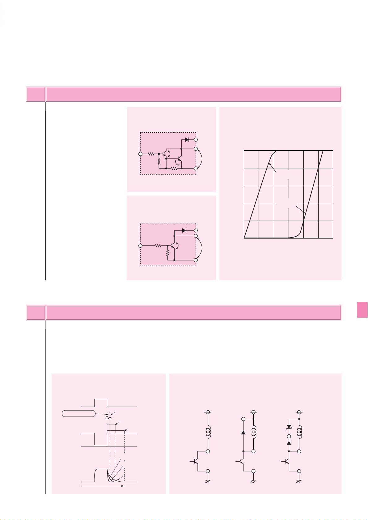
How to use
Mitsubishi transistor array is a semiconductor integrated circuit formed of 4 to 8 circuits containing transistors that
can operate at an output withstand voltage of 30 to 80V and an output current of 50 to 1,500 mA. This transistor
array has a variety of specifications, some of which will be introduced here.
Examples of connections with
C-MOS ICs are shown here.
This type of C-MOS output
current can be either the "sink"
or "source" type. Connection
examples are shown in Figs.
1 and 2.
Fig. 3 shows the internal
circuit of a transistor array
into which an input diode is
built.
Negative voltage can be
applied using this diode.
There are two output current format types, the
current sink type (intake type) and the source
type (supply type). Example applications of
these are shown in Figs. 4 and 5.
Fig. 1. Operating with "H" input
Fig. 3. Negative input applied voltage type
Fig. 2. Operating with "L" input
Output sink, source type
Fig. 4. Output sink type application example
Fig. 5. Output source type application example
Negative input applied voltage type
1
2
3
Direct operation with C-MOS IC
Page 16
16
(a)No clamp diode (b)Clamp diode only (c)Clamp diode
+ Zener
10k
OUT
GND
IN
2.7k
COM
M63813P/FP/GP/KP
VO(@200mA)=VCE(sat)=0.3V
VCE(sat)
VO
OUT
GND
IN
2.7k
7.2k
COM
3k
M63823P/FP/GP
VO(@200mA)=VBE+VCE(sat)=1.0V
VCE(sat)
VBE
VO
Input voltage waveform
L
H
0V
0V
No clamp diode
Clamp diode V
F
Output voltage waveform
Reverse voltage
Output current waveform
Time t
0mA
V
Z+VF
VS
No clamp diode
Clamp diode +
Zener diode
Clamp diode only
OUT
GND
L
V
S
OUT
GND
L
COM
V
S
OUT
GND
L
COM
V
S
250
0
200
150
100
50
Output saturation voltage and collector current characteristics
0 1.21.00.80.60.40.2
Output saturation voltage VCE(sat) (V)
Collector current IC(mA)
M63813
(IB=2mA)
M63823
(II=0.5mA)
The output transistor formats
are the Darlington type and
the single type. The Darlington type shown in Fig. 6
can generate high operation
current from a minute input
current, but the output saturation voltage is 0.95 to
1.05V. The single type shown
in Fig. 7 can keep the saturation voltage low. The output saturation voltage and
collector current characteristics of these two types are
shown in Fig. 8.
Fig. 6. Darlington type
Fig. 8. Output saturation voltage and
collector current characteristics
Fig. 7. Single type
4
Low output saturation type
Fig. 9. Output voltage and current waveform
during L load operation
Fig. 10. Method for protecting the transistor during L load operation
5
Built-in output clamp diode type
When operating under an inductive(L) load, such as a relay or
motor, the built-in clamp diode shown in Fig. 10(b) is used to
protect the circuit from the reverse voltage that occurs when
the transistor array is turned off.
When only the clamp diode is connected, the flow time of the
current in the clamp diode is long and the switching sometimes
deteriorates a little for relays, etc. as shown in Fig. 9.
When this is a problem, a Zener diode is inserted at the clamp
diode COM terminal(in reverse series) as shown in Fig. 10(c)
to improve the current smooth flow. The Zener diode voltage
(Vz) should be selected such that V
S
+ VZ + VF < V
BR(CEO)
and a voltage type Zener should be used.
Page 17
17
M
M
Vs
Electronic chime
Micro
-computer
Opto isolator
Power relay
Vcc
M63823GP
M63823GP
8
10
12
13
14
15
11
16
7
5
4
3
2
6
1
9
8
10
12
13
14
15
11
16
7
5
4
3
2
6
1
9
Stepping motor
Stepping motor
LEDs
M
M
Micro
-computer
Vs
M63823GP
8
10
12
13
14
15
11
16
7
5
4
3
2
6
1
9
Vcc
M63823GP
8
10
12
13
14
15
11
16
7
5
4
3
2
6
1
9
Stepping motor
Stepping motor
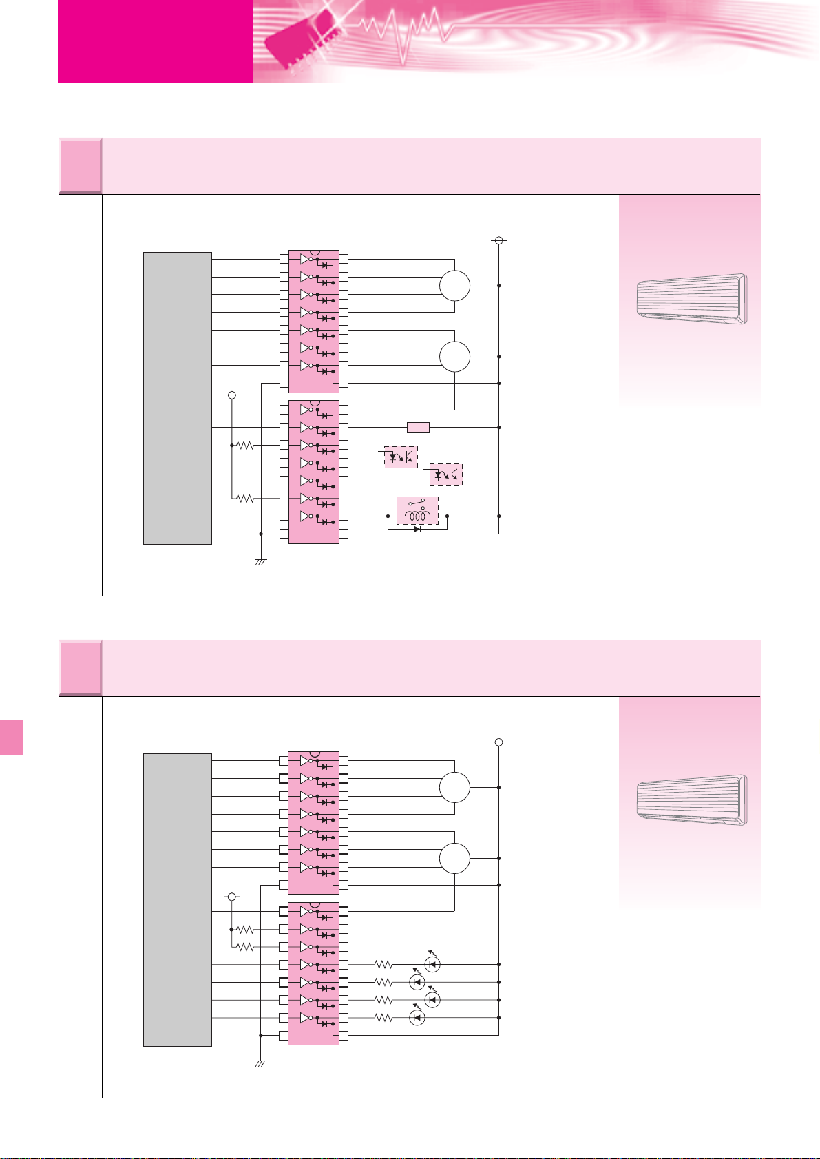
Air conditioner example 2 [Internal unit
]
Application examples
Air conditioner example 1 [Internal unit
]
Page 18
18
Vcc
Vs1
Vs2
Micro
-computer
M54566P/FP
M54583P
8
10
12
13
14
15
11
16
7
5
4
3
2
6
1
9
8
10
12
13
14
15
11
16
17
18
7
5
4
3
2
6
1
9
Power relay
Solenoid valve
Dry
Hand
wash
Blanket
Standard
Slightly dirty
Let soak
8
10
12
13
14
15
11
16
7
5
4
3
2
6
1
9
8
10
12
13
14
15
11
16
17
18
7
5
4
3
2
6
1
9
Vcc
M63823P
8
10
12
13
14
15
11
16
7
5
4
3
2
6
1
9
Display panel
Motors and
solenoids drives
Tr iac gate drive
M63823P
Micro
-computer
M54563P
High
Medium
Low
Small
Ver y small
Wash
14 m in
10 m in
8 min
5 min
Rinse
Add water
3 times
2 times
1 times
Spin
6 min
4 min
2 min
Wrinkle reduction
Time remaining
Inspection
min after
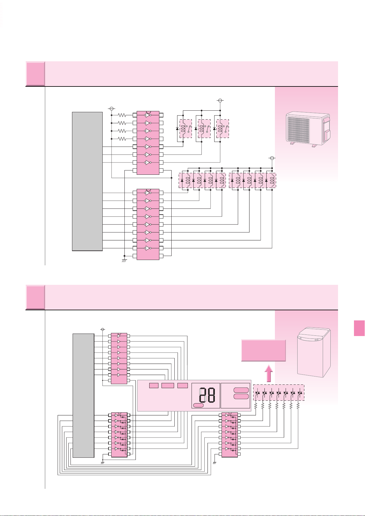
Air conditioner example 3 [External unit
]
Washing machine
Page 19

19
M63826P
M63823P
M54562P
Power relay
Vcc
Micro
-computer
8
10
12
13
14
15
11
16
7
5
4
3
2
6
1
9
8
12
13
14
15
16
5
4
3
2
1
9
8
10
12
13
14
15
11
16
17
18
7
5
4
3
2
6
1
9
Vcc
Vs
Micro
-computer
LEDs
Power relay
Temperature
LEDs
7
6
10
11
Fan heater
Application examples
Refrigerator
Page 20
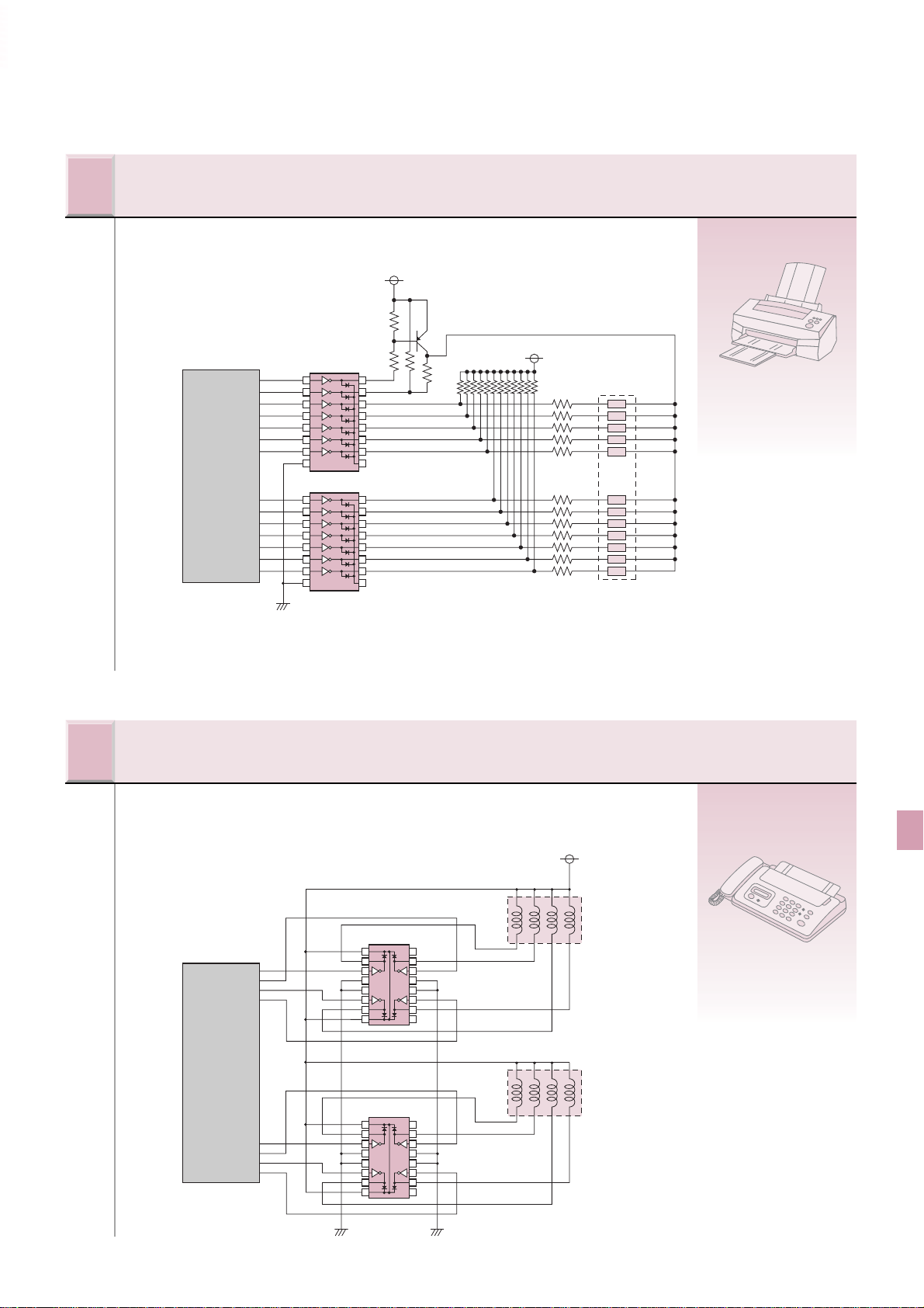
Ink jet printer
Micro
-computer
M63823P
1
2
3
4
5
6
7
8
M63823P
2
3
4
5
6
7
8
Vcc
Vcc
16
15
14
13
12
11
10
9
161
15
14
13
12
11
10
9
Ink jet cartridge
electrode
Fax
Micro
-computer
M54532P
16
1
15
2
14
3
13
4
12
5
11
6
10
7
9
8
M54532P
16
1
15
2
14
3
13
4
12
5
11
6
10
7
9
8
Original paper feed
stepping motor
Recording paper feed
stepping motor
Vcc
20
Page 21
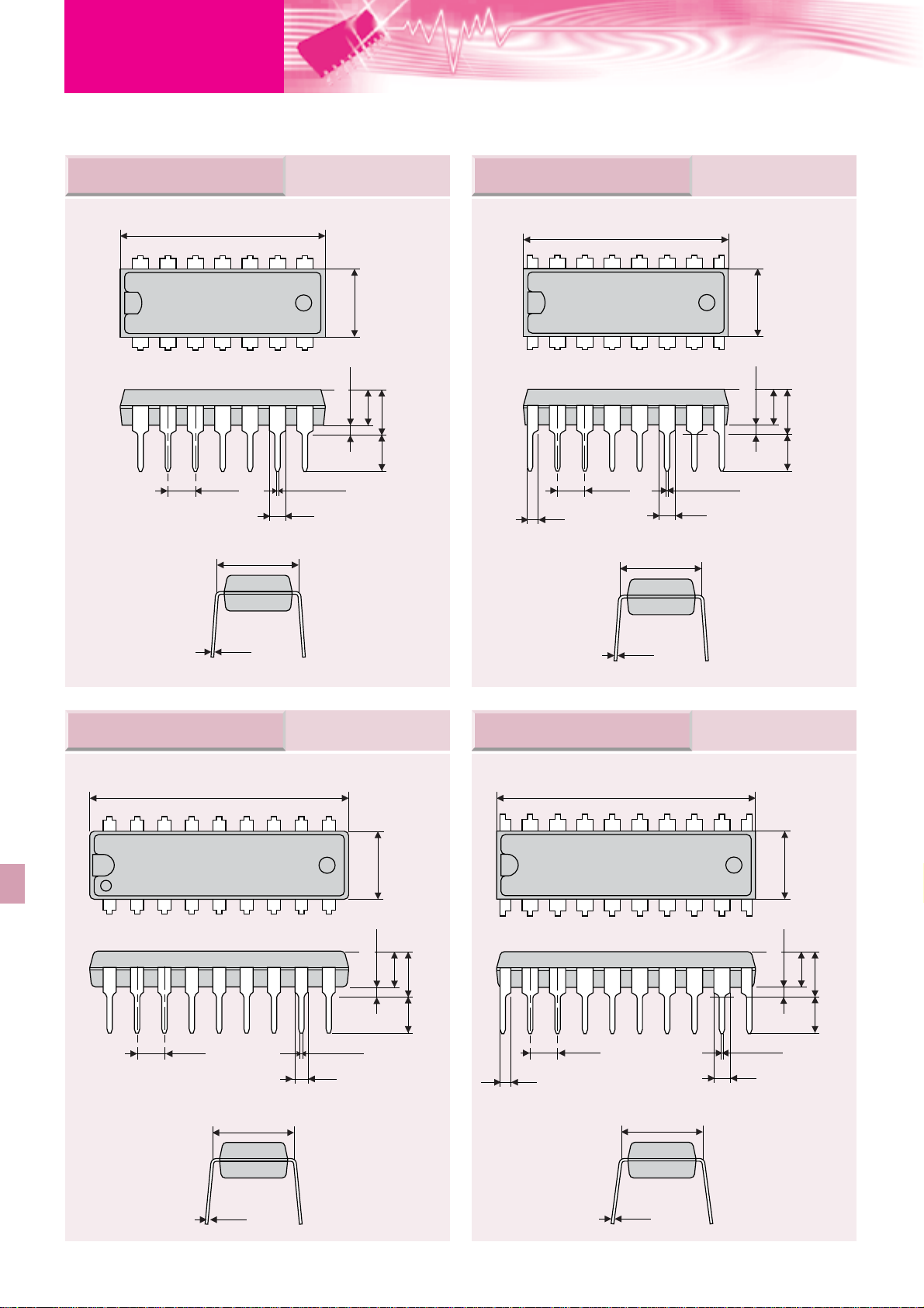
Package outlines
Unit : mm
TYPE 14P4 TYPE 16P4
19± 0.2
14pin 300mil DIP 16pin 300mil DIP
19± 0.2
6.3± 0.15
0.51MIN.
3.3
4.5MAX.
3MIN.
+0.3
–
2.54
0.1
2.54
±0.1
0.5
+0.3
1.5
–
0.1
1.0
7.62
7.62
1.5
0.5± 0.1
+0.3
–
0.1
6.3± 0.15
0.51MIN.
3.3
4.5MAX.
3MIN.
+0.0 7
0.27
–
0.05
TYPE 18P4G TYPE 20P4
18pin 300mil DIP
24±0.2
0.27
24±0.2
6.3± 0.15
0.51MIN.
3.3
4.5MAX.3MIN.
+0.3
–
2.54
0.1
2.54
1.2
0.5± 0.1
+0.3
0.1
–
1.0
+0.0 7
–
0.05
20pin 300mil DIP
6.3± 0.15
0.51MIN.
3.3
4.5MAX.
3MIN.
0.5± 0.1
+0.3
1.5
–
0.1
21
0.25
+0.0 7
–
0.05
7.62
0.27
+0.0 7
–
0.05
7.62
Page 22

Unit : mm
TYPE 16P2N TYPE 16P2S
10.1±0.1
1.27
0.1±0.1
A
2.1MAX.
1. 2 5
16pin 300mil SOP
5.3± 0.1
1.8
+0.1 0
0.4
– 0.05
7. 8 ± 0.3
10± 0.2
1.27
+0.1 0
0.4
– 0.05
TYPE 16P2Z
+0.05
0.2
–
0.02
Detail A
TYPE 20P2N
12.6± 0.1
4°±4°
0.6 ±0.2
20pin 300mil SOP
0.65
5± 0.2
0.22
+0.1 0
– 0.05
4.4± 0.2
1.5
16pin 225mil SOP
0.05MIN.
4.4± 0.2
A
1.9MAX.
1.5
+0.0 5
0.15
0.02
–
Detail A
6.2± 0.3
0.9
0° to 10°
0.4± 0.2
16pin 225mil SSOP
0.05MIN.
6.2± 0.3
0.15
A
1.9MAX.
+0.0 5
0.02
–
0.9
0° to 10°
0.4± 0.2
0.2
A
+0.05
0.02
–
Detail A
2.1MAX.
1.27
0.1±0.1
Detail A
5.3± 0.11.8
TYPE 20P2E
+0.1 0
0.4
– 0.05
6.5±0.1
0.22
4.4±0.1
1.15
+0.10
–0.05
7. 8 ± 0.3
1. 2 5
0.65
4°±4°
0.6 ±0.2
20pin 225mil SSOP
±0.1
0.1
6.4±0.2
A
+0.05
–0.02
Detail A
1.0
0° to 10°
1.45MAX.
0.15
0.5±0.2
22
 Loading...