


C
MIT
SUBIS
C
HI ELECTRI
MELSEC System Q
Programmable Logic Controllers
User's Manual
Art. no.: 130383
01 05 2003
SH(NA)-080042
Version L
Digital I/O Modules
QX
MITSUBISHI ELECTRI
/QY
INDUSTRIAL AUTOMATION
SAFETY PRECAUTIONS •
•
(Always read these instructions before using this equipment.)
Before using this product, please read this manual and the relevant manuals introduced in this manual
carefully and pay full attention to safety to handle t he product correctly .
The instructions given in this manual are concerned with this product. For the safety instructions of the
programmable controller system, please read the CPU module user's manual.
In this manual, the safety instructions are ranked as "DANGER" and "CAUTION".
DANGER
!
CAUTION
!
Note that the !CAUTION level may lead to a serious consequence according to the circumstances.
Always follow the instructions of both levels because they are important to personal safety .
Please save this manual to make it accessible when required and always forward it to the end user.
Indicates that incorrect handling may cause hazardous conditions,
resulting in death or severe injury.
Indicates that incorrect handling may cause hazardous conditions,
resulting in medium or slight personal injury or physical damage.
[Design Instructions]
!
DANGER
• Install a safety circuit external to the PLC that keeps the ent ire syst em safe if there are problems
with the external power supply or PLC. Not doing so may cause false output or malfunction,
leading to accidents.
(1) Outside the PLC, construct mechanical damage preventing interlock circuits, e.g. emergency
stop circuits, protective circuits, forward/rev erse or other conflicting operation interlocking
circuits, and upper and lower positioning limit switches.
(2) When the PLC detects either of the following problems, it will stop arithmet ic operat ion and
turn off all outputs in the case of (a). In the case of (b) , it will st op arithmet ic operation and
hold or turn off all outputs according to the parameter setting.
(a) The overcurrent protection or overvoltage protection of the pow er supply module is
activated.
(b) The self-diagnostic function of the PLC CPU has detected a fault such as the watchdog
timer error.
In addition, all outputs may be turned on when there are problems undetectable by the PLC
CPU, such as in the I/O controller. Build a fail-safe circuit or provide a mechanism externally
of the PLC to operate the machine safely at such times. Refer to the CPU module user's
manual for fail-safe circuit examples.
(3) Output could be left on or off when there is trouble in the output module's relays, t ransistors,
etc. So build an external monitoring circuit that will monito r any output signal that could lead
to a serious accident.
A - 1 A - 1
[Design Instructions]
!
DANGER
• When overcurrent exceeding the rated load current or caused by a shorted load or the like flows
in the output module for a long time, it may cause smoke or fire. To prevent this, configure an
external safety circuit, such as fuses.
• Build a circuit that turns on the external power supply after the PLC pow er supply has been
turned on. If the external power supply is turned on first, it could result in false output or
malfunction.
• When there are communication problems with the data link, refer to the corresponding data link
manual for the operating status of each station. Not doing so could result in false output or
malfunction.
• When connecting a peripheral device to the CPU module or connecting a personal computer or
the like to the intelligent function module to exercise control (data change) on the running PLC,
configure up an interlock circuit in the sequence program to ensure that t he whole sy stem w ill
always operate safely.
Also before exercising other control (program change, operating status change (status control))
on the running PLC, read the manual carefully and fully confirm safety.
Especially for the above control on the remote PLC from an external device, an immediate
action may not be taken for PLC trouble due to a data communication fault.
In addition to configuring up the interlock circuit in the sequence program, corrective and other
actions to be taken as a system for the occurrence of a data communication fault should be
predetermined between the external device and PLC CPU.
!
CAUTION
• Do not bundle the control wires or communication cables with the main circuit or power wires, or
run them close to each other.
They should be run 100mm (3.94in.) or more away from each other.
Not doing so could result in noise that would cause malfunction.
• When the output module is used to control a lamp load, heater, solenoid valve or the like, large
current (approximately 10 times greater than the normal) may flow when the output is turned
from OFF to ON. Choose an output module having a sufficient rated current.
A - 2 A - 2
[Installation Instructions]
!
CAUTION
• Use the PLC in the environment that meets the general specifications given in t his manual.
Using this PLC in the environment outside the range of the general specifications could result in
electric shock, fire, malfunction, or damage to, or deterioration of the product.
• Hold down the module-loading lever at the module bottom, and securely insert the module-fixing
hook into the fixing hole in the base unit. Incorrect loading of the module can cause a
malfunction, failure or drop.
When using the PLC in the environment of much vibration, tighten the module with a screw.
Tighten the screw in the specified torque range. Undertightening can cause a drop, short circuit
or malfunction. Overtightening can cause a drop, short circuit or malfunction due to damage to
the screw or module.
• When installing extension cables, be sure that the connectors of base unit are installed correctly.
After installation, check them for looseness. Poor connections could cause an input or output
failure.
• Securely load the memory card by pushing it into the memory card loading connector. After
loading, make a check. Not doing so can cause malfunction due to a contact fault.
• Completely turn off the external power supply before loading or unloading the module. Not doing
so could result in damage to the product.
• Do not directly touch the module's conductive parts.
Doing so could cause malfunction or failure of the module.
[Wiring Instructions]
!
DANGER
• Completely turn off the external power supply before starting wiring. Not doing so could result in
electric shock or damage to the product.
• When turning on the power supply or starting operation after wiring work, always mount the
product with the supplied terminal cover.
Not doing so could result in electric shock.
A - 3 A - 3
[Wiring Instructions]
!
CAUTION
• Always ground the FG and LG terminals to the protectiv e ground conductor. Not doing so could
result in electric shock or malfunction.
• Before wiring the module, confirm the rated voltage and terminal layout of the product.
Connecting a power supply that is different from the rating or incorrectly wiring the product could
result in fire or failure.
• External connectors should be crimped or pressure-welded with the specified tools, or correctly
soldered. Imperfect connections could result in short circuit, fires or malfunction.
• Tighten the terminal screws in the specified torque range.
Undertightening could result in short circuit, fire or malfunction.
Overtightening could cause damage to the screws and/or the module, resulting in drop, short
circuit or malfunction.
• Be careful not to allow foreign matter such as chips and wire off-cuts to enter the module.
Foreign matter could cause fire, failure, or malfunction.
• The module has an ingress prevention label on its top to prevent foreign matter, such as wire
offcuts, from entering the module during wiring.
Do not peel this label during wiring.
Before starting system operation, be sure to peel this label because of heat dissipation.
[Startup/Maintenance Instructions]
!
DANGER
• Do not touch the terminals while power is on.
Doing so could cause electric shock.
• Correctly connect the battery. Do not charge, disassemble, heat, place in fire, short circuit, or
solder the battery.
Mishandling of the battery can cause heat generation, burst or ignition which could result in
injury or fire.
• Always turn off the external power supply completely before cleaning the module or retightening
the terminal or module mounting screws.
Not doing so could result in electric shock.
Undertightening of terminal screws can cause a short circuit or malfunction.
Overtightening of screws can cause damage to the screws and/or the module, resulting in drop,
short circuit, or malfunction
A - 4 A - 4
[Startup/Maintenance Instructions]
!
CAUTION
• The online operations conducted for the running CPU module by connecting a peripheral device
(especially program modification, forced output, operating status change) should be performed
after you have read the manual carefully read and fully confirmed safety.
Operation mistakes could cause machine damage or accident.
• Do not disassemble or modify the modules.
Doing so could cause failure, malfunction, injury or fire.
• Always switch off the external power supply completely before mounting or removing the
module.
Not doing so can cause failure or malfunction of the module.
• Before touching the module, always touch grounded metal, etc. to discharge st atic elect ricity
from human body, etc.
Not doing so can cause the module to fail or malfunction.
[Disposal Instructions]
!
CAUTION
• When disposing of this product, treat it as industrial waste.
A - 5 A - 5
REVISIONS
The manual number is given on the bottom left of the back cover.
Print Date Manual Number Revision
Dec., 1999 SH (NA)-080042-A First edition
Feb., 2000 SH (NA)-080042-B
Addition model
QH42P, QX48Y57, QX70, QX71, QX72, QY18A
Addition
Chapter 4
Partial correction
Section 1.2, Chapter 5, 8.1,
Chapters 4 to 8 (changed into Chapters 5 to 9)
Apr., 2000 SH (NA)-080042-C
Deletion
QY18A
Jul., 2000 SH (NA)-080042-D
Addition model
QX28,QX40-S1,QY18A,QY22,QI60
Addition
Chapter 5
Partial correction
Section 1.2
Chapters 5 to 9 (changed into Chapters 6 to 10)
Nov., 2000 SH (NA)-080042-E
Addition model
QY70, QY71
Addition
Section 1.3
Partial correction
CONTENTS, Section 3.3, 5.1
Jan., 2001 SH (NA)-080042-F
Addition model
QY68A
Addition
Section 10.2
Partial correction
CONTENTS, Section 1.2, 3.3, 5.1, Chapters 7
Mar., 2001 SH (NA)-080042-G
Partial correction
Section 2.4, 8.1
Jul., 2001 SH (NA)-080042-H
Addition model
Q6TE-18S
Addition
Chapter 9, APP 1.3
Partial correction
CONTENTS, Section 2.1, 2.2, 2.4, 5.1
Chapters 9 to 10 (changed into Chapters 10 to 11)
Jul., 2002 SH (NA)-080042-I
Addition model
QX41-S1, QX42-S1, A6CON4
This manual confers no industrial property rights or any rights of any other kind, nor does it confer any patent licenses.
Mitsubishi Electric Corporation cannot be held responsible for any problems involving industrial property rights which
may occur as a result of using the contents noted in this manual.
1999 MITSUBISHI ELECTRIC CORPORATION
Japanese Manual Version SH-080024-L
A - 6 A - 6
Print Date Manual Number Revision
Mar., 2003 SH (NA)-080042-J
Addition model
QX82
May., 2003 SH (NA)-080042-K
Partial correction
Section 1.2, 2.2
May., 2003 SH (NA)-080042-L
Addition model
QX82-S1
Partial correction
Section 1.2, 3.3
Addition
Section 2.15
A - 7 A - 7

INTRODUCTION
Thank you for choosing the MITSUBISHI MELSEC-Q Series General-Purpose Programmable Logic Controller.
Before using this product, please read this manual carefully to use the equipment to its optimum.
CONTENTS
About Manuals ..............................................................................................................................................A- 10
1. GENERAL SPECIFICATIONS OF INPUT AND OUTPUT MODULES AND INSTRUCTIONS FOR
SELECTING THEM 1- 1 to 1- 12
1.1 General Specifications............................................................................................................................1- 1
1.2 Selecting Instructions..............................................................................................................................1- 1
1.3 How to Make Settings on GX Developer.................................................................................................1- 8
1.3.1 Setting of I/O response time .............................................................................................................1- 8
1.3.2 Setting of error-time output mode.....................................................................................................1-10
1.3.3 QI60 switch setting............................................................................................................................1-11
2. INPUT MODULE SPECIFICATIONS 2- 1 to 2-18
2.1 QX10 AC Input Module...........................................................................................................................2- 1
2.2 QX28 AC Input Module...........................................................................................................................2- 2
2.3 QX40 DC Input Module (Positive Common Type).................................................................................2- 3
2.4 QX40-S1 DC Input Module (Positive Common Type)...........................................................................2- 4
2.5 QX41 DC Input Module (Positive Common Type).................................................................................2- 5
2.6 QX41-S1 DC Input Module (Positive Common Type)...........................................................................2- 6
2.7 QX42 DC Input Module (Positive Common Type).................................................................................2- 8
2.8 QX42-S1 DC Input Module (Positive Common Type)...........................................................................2- 9
2.9 QX70 DC Input Module (Positive Common/Negative Common Shared Type)....................................2-11
2.10 QX71 DC Input Module (Positive Common/Negative Common Shared Type)..................................2-12
2.11 QX72 DC Input Module (Positive Common/Negative Common Shared Type)..................................2-13
2.12 QX80 DC Input Module (Negative Common Type)..............................................................................2-14
2.13 QX81 DC Input Module (Negative Common Type)..............................................................................2-15
2.14 QX82 DC Input Module (Negative Common Type)..............................................................................2-16
2.15 QX82-S1 DC Input Module (Negative Common Type) ........................................................................2-17
3. OUTPUT MODULE SPECI FI CA TIO NS 3- 1 to 3- 1 3
3.1 QY10 Contact Output Module ................................................................................................................3- 1
3.2 QY18A Contact Output Module (All Points Independent) .....................................................................3- 2
3.3 QY22 TRIAC Output Module..................................................................................................................3- 3
3.4 QY40P Transistor Output Module (Sink Type) ......................................................................................3- 4
3.5 QY41P Transistor Output Module (Sink Type) ......................................................................................3- 5
3.6 QY42P Transistor Output Module (Sink Type) ......................................................................................3- 6
3.7 QY50 Transistor Output Module (Sink Type).........................................................................................3- 7
3.8 QY68 Transistor Output Module (All Points Independent, Sink/Source Type)..................................... 3- 8
3.9 QY70 Transistor Output Module (Sink Type).........................................................................................3- 9
3.10 QY71 Transistor Output Module (Sink Type)........................................................................................3-10
3.11 QY80 Transistor Output Module (Source Type)...................................................................................3-11
A - 8 A - 8

3.12 QY81P Transistor Output Module (Source Type)................................................................................. 3-12
4. INPUT/OUTPUT CONPOSITE MODULE 4- 1 to 4- 4
4.1 QH42P I/O Module..................................................................................................................................4- 1
4.2 QX48Y57 I/O Module..............................................................................................................................4- 3
5. INTERRUPT MODULE 5- 1 to 5- 2
5.1 QI60 Interrupt Module.............................................................................................................................5- 1
6. BLANK COVER MODULE 6- 1 to 6- 2
7. CONNECTORS 7- 1 to 7- 2
8. SPECIFICATIONS OF CONNECTOR/TERMINAL BLOCK CONVERTOR MODULES 8- 1 to 8- 7
8.1 Specifications of Connector/Terminal Block Convertor Modules..........................................................8- 1
8.2 Connector/Terminal Block Convertor Module Connection Diagrams...................................................8- 3
8.2.1 A6TBXY36........................................................................................................................................8- 3
8.2.2 A6TBXY54........................................................................................................................................8- 4
8.2.3 A6TBX70 ..........................................................................................................................................8- 5
8.2.4 A6TBX36-E.......................................................................................................................................8- 5
8.2.5 A6TBY36-E.......................................................................................................................................8- 6
8.2.6 A6TBX54-E.......................................................................................................................................8- 6
8.2.7 A6TBY54-E.......................................................................................................................................8- 7
8.2.8 A6TBX70-E.......................................................................................................................................8- 7
9. SPRING CLAMP TER MINAL BL OCK 9- 1 to 9- 2
9.1 Q6TE-18S.............................................................................................................................................9- 1
10. NAMES OF MODULE PARTS 10- 1 to 10- 4
11. I/O MODULE TROUBLESHOOTING 11- 1 to 11- 4
11.1 Input Circuit Troubleshooting..............................................................................................................11- 1
11.2 Output Circuit Troubleshooting...........................................................................................................11- 4
APPENDICES App- 1 to App- 9
Appendix 1 External Dimensional Drawings............................................................................................App- 1
Appendix 1.1 I/O modules.....................................................................................................................App- 1
Appendix 1.2 Connectors, connector/terminal block converter modules............................................App- 4
Appendix 1.3 Spring Clamp Terminal Block..........................................................................................App- 7
Appendix 2 Compatibility with MELSEC-AnS Series I/O modules..........................................................App- 8
A - 9 A - 9
About Manuals
The following manuals are also related to this product.
In necessary, order them by quoting the details in the tables below.
Related Manuals
Manual Name
Basic model QCPU (Q Mode) User's M anual (Hardware Design/Maintenance and Inspection)
This manual provides the specifications of the CPU modules, power supply modules, base units, extension
cables, memory cards and others. (Optional)
Manual Number
(Model Code)
SH-080187
(13JR43)
Basic model QCPU (Q Mode) User's M anual (Function Explanation/Program Fundamentals)
This manual explains the functions, programming methods, devices and so on necessary to create programs
with the QCPU (Q mode). (Optional)
High Performance model QCPU (Q Mode) User's M anual (H ardw are D esign/Maintenance and
Inspection)
This manual provides the specifications of the CPU modules, power supply modules, base units, extension
cables, memory cards and others. (Optional)
High Performance model QCPU (Q Mode) User's M anual (Function Explanation/Program
Fundamentals)
This manual explains the functions, programming methods, devices and so on necessary to create programs
with the QCPU (Q mode). (Optional)
SH-080188
(13JR44)
SH-080037
(13JL97)
SH-080038
(13JL98)
Conformation to the EMC Directive and Low Voltage Instruction
For details on making Mitsubishi PLC conform to the EMC directive and low voltage instruction when installing
it in your product, please refer to Chapter 3, "EMC Directive and Low Voltage Instruction" of the PLC CPU
User's Manual(Hardware).
The CE logo is printed on the rating plate on the main body of the PLC that conforms to the EMC directive and
low voltage instruction.
A - 10 A - 10
1 GENERAL SPECIFICATIONS OF INPUT AND OUTPUT MODULES AND
INSTRUCTIONS FOR SELECTING THEM
MELSEC-Q
1. GENERAL SPECIFICATIONS OF INPUT AND OUTPUT MODULES AND INSTRUCTIONS FOR SELECTING THEM
This chapter describes the general specifications of I/O modules and instructions for
selecting them.
1.1 General Specifications
Refer to the following manual for the general specifications of the I/O modules.
• Basic model QCPU (Q Mode) User's Manual (Hardware Design/Maintenance and
Inspection)
• High Performance model QCPU (Q Mode) User's Manual (Hardware Design/
Maintenance and Inspection)
1.2 Selecting Instructions
(1) If an output module drives an inductive load, it must be switched ON for 1 second
or longer and switched OFF for 1 second or longer.
(2) If a counter or timer which has a DC-DC converter as a load is used with an output
module, using an average current to choose an output module can cause a fault
due to periodic rush currents when it is turned ON or during operation.
To reduce the influence of rush currents for use of the above load, connect a
resistor or an inductance to the load in series or use a module whose maximum
load current is larger.
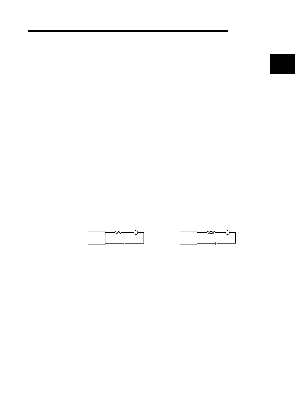
Resistor Load Inductance
Output
module
(3) Fuses installed in output modules cannot be replaced. They are designed to protect
external wiring if the module outputs are shorted.
Therefore, output modules may not be protected from a short circuit.
If an output module becomes faulty due to any cause other than a short circuit, its
fuse may not function.
(4) The number of signals, which can be turned ON simultaneously in an input module,
varies according to the input voltage and ambient temperature.
Refer to the corresponding input module specifications.
Output
module
Load
1
1 - 1 1 - 1
1 GENERAL SPECIFICATIONS OF INPUT AND OUTPUT MODULES AND
INSTRUCTIONS FOR SELECTING THEM
1
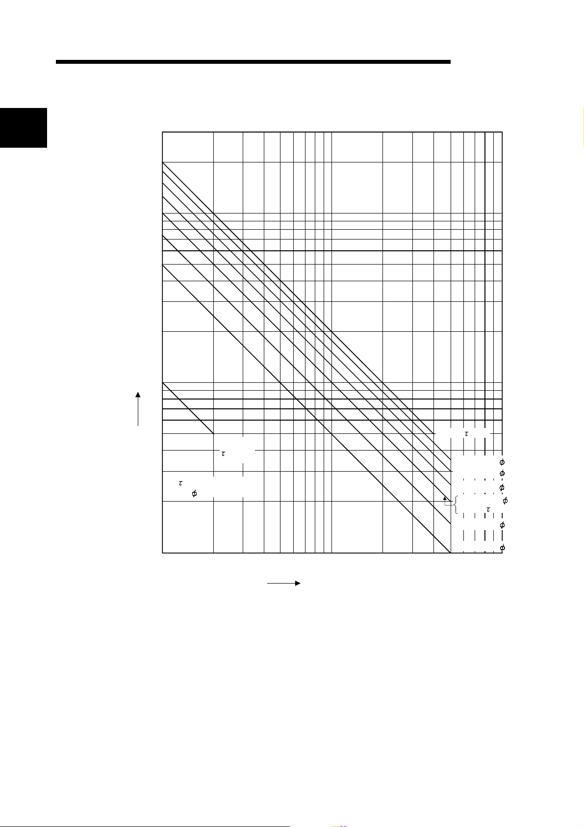
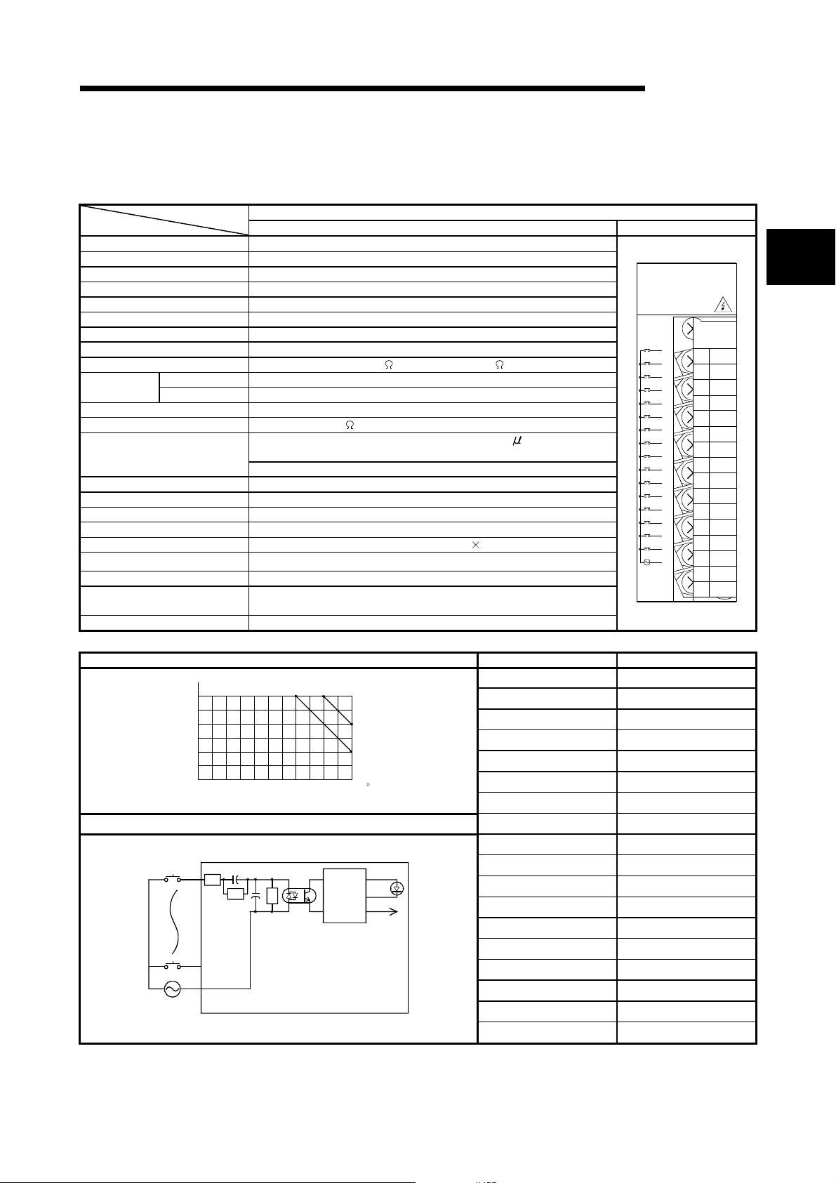
(5) The following chart shows the service life of a relay output module.
Applicable module: QY10, QY18A
MELSEC-Q
200
100
70
50
30
20
10
Switching life (10,000 times)
7
5
3
(L/R): Time constant
cos : Power factor
2
DC100
=7ms
DC30V =0ms
AC100V cos =0.7
AC200V cos =0.7
AC100V cos =0.35
AC200V cos =0.35
DC24V =7ms
AC120V cos =0.2
1
0.1 0.2 0.3 0.5 0.7 1 2 3 5
Switching current (A)
AC240V cos =0.2
1 - 2 1 - 2

1 GENERAL SPECIFICATIONS OF INPUT AND OUTPUT MODULES AND
INSTRUCTIONS FOR SELECTING THEM
POINT
(1) When using the module for the application in which the relay contact is
frequently switched, the relay life span should be considered. Therefore, it is
recommended to use a triac output module.
(2) The relay life curve shows the value based on actual use, which is not
guaranteed. Therefore, make sure to allow for a margin of error.
The relay life span differs according to the specifications as follows:
Rated switching voltage, current load 100 thousand operations
200V AC 1.5A, 240V AC 1A (COS
200V AC 0.4A, 240V AC 0.3A (COS
200V AC 1A, 240V AC 0.5A (COS
200V AC 0.3A, 240V AC 0.15A (COS
24V DC 1A, 100V DC 0.1A (L/R=7ms) 100 thousand operations
24V DC 0.3A, 100V DC 0.03A (L/R=7ms) 300 thousand operations
(3) Relay life is substantially affected by the load type and inrush current
characteristics.
The inrush current may cause the contact welding. Therefore, consideration
should be given to it as well as constant current.
(a) Inductive load
When the inductive load such as electromagnetic contactor or solenoid is
shut off, high counter-electromotive force is generated between the
contacting materials to produce an arc discharge. Consideration should be
made especially when the power factor is low, as it may decrease the life
period.
In addition, make sure to consider the contact melting, as the inrush current
equivalent to 5 to 15 times of constant current flows when the module is
powered on.
(b) Lamp load
Make sure to consider the contact melting, as the inrush current equivalent
to 10 to 15 times of constant current flows in the lamp circuit.
(c) Capacitive load
Make sure to consider the contact melting when a device such as condenser
is used in a load circuit, as the inrush current equivalent to 20 to 40 times of
constant current may flow in the circuit.
Also, pay full attention to the wire capacity if long length of wire is routed.
(6) Insulation-sleeved crimping terminals cannot be used with the terminal block.
It is recommended to cover the wire connections of the crimping terminals with
mark or insulation tubes.
(7) Use wires of 0.3 to 0.75mm
terminal block.
(8) Do not use I/O modules under pressure higher than the atmospheric pressure of
0m (0ft.) altitude. Doing so can cause a malfunction.
When using I/O modules under pressure, please consult your sales representative.
=0.7) 100 thousand operations
=0.7) 300 thousand operations
=0.35) 100 thousand operations
=0.35) 300 thousand operations
2
core and 2.8mm (0.11in.) OD max. to connect to the
MELSEC-Q
1 - 3 1 - 3
1 GENERAL SPECIFICATIONS OF INPUT AND OUTPUT MODULES AND
INSTRUCTIONS FOR SELECTING THEM
(9) Tighten the module fixing and terminal block screws to the torques in the following
ranges.
Screw Location Tightening Torque Range
Module fixing screw (M3 12 screw) 36 to 48 N•cm
I/O module terminal block screw (M3 screw) 42 to 58 N•cm
I/O module terminal block mounting screw (M3 screw) 66 to 89 N•cm
(10)There are the following restrictions on the thermal protections activated by
protected output modules.
The thermal protections are overload and overheat protective functions.
(a) QY40P, QY41P, QY42P, QH42P
Function Description
Common
(Overload and overheat
protective functions)
Overload protective
function
Overheat protective
function
• If an overcurrent keeps flowing due to overload, heat is generated
to activate the overheat protective function.
• Each protective function is designed to protect the internal
elements of the module, not the external equipment.
• The overload protective function is activated in 1 point increments
in terms of 1A to 3A/point.
• The overload protective function returns operation to normal when
the load becomes a rated load
• The overheat protective function is activated in 1 point increments.
• The overheat protective function automatically returns operation to
normal when heat reduces.
MELSEC-Q
1 - 4 1 - 4
1 GENERAL SPECIFICATIONS OF INPUT AND OUTPUT MODULES AND
INSTRUCTIONS FOR SELECTING THEM
(b) QY81P
Function Description
Common
(Overload and overheat
protective functions)
Overload protective
function
Overheat protective
function
• If an overcurrent keeps flowing due to overload, heat is generated
to activate the overheat protective function.
• Each protective function is designed to protect the internal
elements of the module, not the external equipment.
• The overload protective function is activated in 1 point increments
in terms of 1A to 3A/point.
• The overload protective function returns operation to normal when
the load becomes a rated load.
• The overheat protective function is activated in 2 point increments.
(It is activated in 2 point increments of Y0/Y1, Y2/Y 3, ..., and w hen
overheat protection is activated, that of 2 points is activated
simultaneously. If an overheat condition persists, heat transferred
may activate the other overheat protective function.)
• If an output turns ON at the activation of the overheat protective
function, the actual output voltage oscillates between 0V and load
voltage.
At the load voltage of 24V, the average voltage during oscillation is
approx. 7V.
No oscillation is encountered when the output is OFF at the
activation of the overheat protective function.
To ensure that the output is turned OFF at the activation of the
overheat protective function, use an external load which sw itches
OFF at 7V or more.
• The overheat protective function automatically returns operation to
normal when heat reduces.
(11)Input modules may import noise or the like as an input depending on the pulse
width of a signal.
This pulse width has a value as listed below depending on the parameter-set
response time. The operating environment should be fully considered when making
the response time setting.
Response Time Setting (ms)
1 0.3
5 3
10 6
20 12
70 45
Minimum Value of Pulse Width
That May Be Imported (ms)
MELSEC-Q
1 - 5 1 - 5
1 GENERAL SPECIFICATIONS OF INPUT AND OUTPUT MODULES AND
INSTRUCTIONS FOR SELECTING THEM
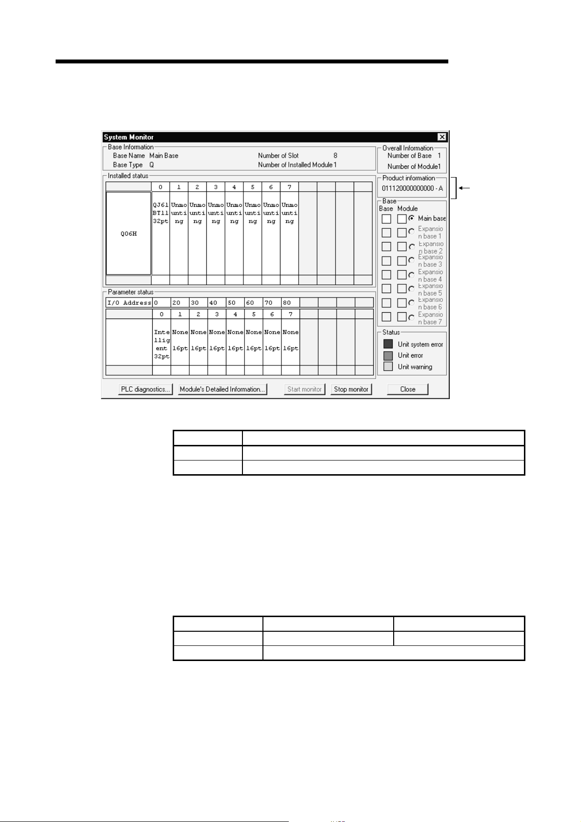
(12)When confirming the product information on the CPU PLC, observe the system
monitor in the DIAGNOSIS menu of the GX Developer.
MELSEC-Q
Confirm by
observing here.
(13)When using the QH42P or QX48Y57, configure it with the following devices.
Part name Detail
CPU PLC Product of product information [011120000000000-A] or later
GX Developer
SW5D5C-GPPW or later
The CPU PLCs other than those listed above cannot be used.
When the SW4D5C-GPPW is used, the response time cannot be set
(fixed at 10ms).
Set OUTPUT for the I/O allocation.
(14)Instructions for use of QY22
It is recommended to fit a fuse to each external terminal in order to prevent the
external device and module from being burnt if a load short-circuit occurs.
The fuse recommended for fitting is the one conforming to IEC60127 Sheet 1.
The following fuses have been confirmed by Mitsubishi to operate properly.
Fuse Model 216 02.5 216 002
Rated current 2.5A 2A
Manufacturer Littelfuse, Inc
1 - 6 1 - 6
1 GENERAL SPECIFICATIONS OF INPUT AND OUTPUT MODULES AND
INSTRUCTIONS FOR SELECTING THEM
(15) Caution points when using QY68A
Installing a fuse to the external terminal to prevent burn out of external devices and
modules in the case of a load short is recommended.
A rated voltage 3A fast type fuse is recommended.
Fuses confirmed for operation by this company are listed below.
Fuse Model 216 3.15 312 003
Rated current 3.15A 3A
Manufacturer Littelfuse, Inc
(16) Possible constructions for QI60 compatible time settings
When setting compatible times for QI60, use the constructions listed below.
If using other constructions, compatible times can not be set. (Fixed at 0.2 ms)
Product name Contents
PLC CPU Product information "021120000000000-B" or later
GX Developer SW6D5C-GPPW or later
MELSEC-Q
1 - 7 1 - 7
1 GENERAL SPECIFICATIONS OF INPUT AND OUTPUT MODULES AND
INSTRUCTIONS FOR SELECTING THEM
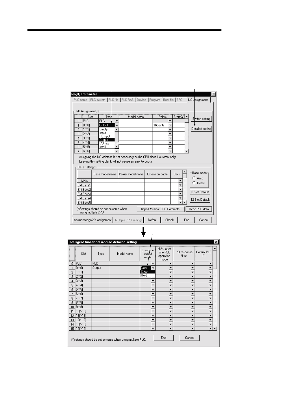
1.3 How to Make Settings on GX Developer
This section describes how to make settings using GX Developer.
1.3.1 Setting of I/O response time
Set the I/O response time in I/O assignment of PLC Parameter.
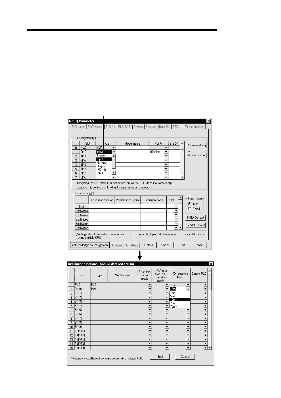
(1) For Input/I/O mix module
Choose [Input/I/O mix] in Type, choose [Detailed setting], and choose [I/O response
time] in I/O response time.
Choose Input/I/O mix.
Choose Detailed setting.
MELSEC-Q
Choose I/O response time
1 - 8 1 - 8
(default: 10ms).
1 GENERAL SPECIFICATIONS OF INPUT AND OUTPUT MODULES AND
INSTRUCTIONS FOR SELECTING THEM
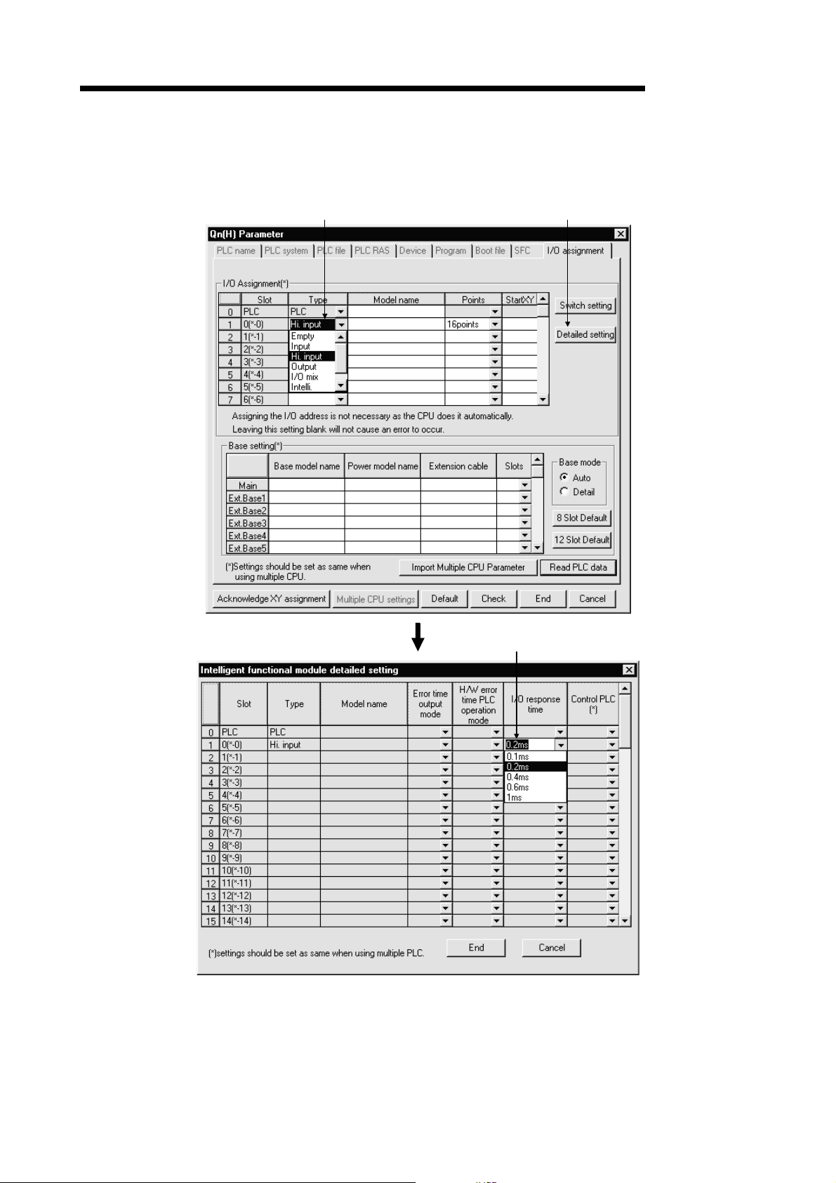
(2) For high-speed input module/QI60
Choose [Hi. input/Interrupt] in Type, choose [Detailed setting], and choose [I/O
response time] in I/O response time.
Choose Hi. input/Interrupt. Choose Detailed setting.
MELSEC-Q
Choose I/O response time
(default: 0.2ms).
1 - 9 1 - 9
1 GENERAL SPECIFICATIONS OF INPUT AND OUTPUT MODULES AND
INSTRUCTIONS FOR SELECTING THEM
1.3.2 Setting of error-time output mode
Set the error-time output mode in I/O assignment of PLC Parameter.
Choose [Output/I/O mix] in Type, choose [Detailed setting], and choose [Clear/Hold] in
Error time output mode.
Choose Output/I/O mix. Choose Detailed setting.
MELSEC-Q
Choose Clear/Hold
(default: Clear).
1 - 10 1 - 10
1 GENERAL SPECIFICATIONS OF INPUT AND OUTPUT MODULES AND
INSTRUCTIONS FOR SELECTING THEM
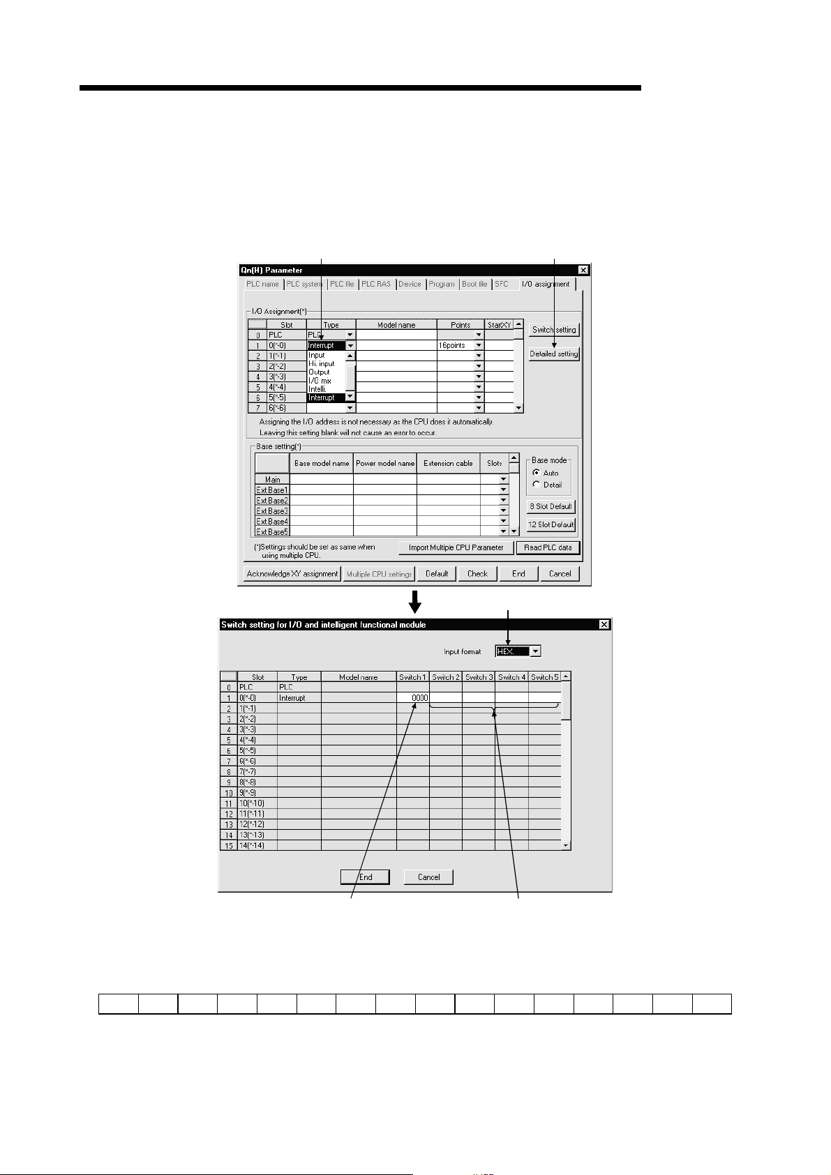
1.3.3 QI60 switch setting
Set the QI60 switches in I/O assignment of PLC Parameter.
Choose [Interrupt] in Type, choose [Switch setting], choose [HEX.] in Input format, and
set the interrupt processing conditions in Switch 1.
Choose Interrupt. Choose Switch setting.
MELSEC-Q
Choose HEX.
Set the interrupt processing conditions
(leading edge/trailing edge) of CH1 to CH16.
Setting inhibited.
Set the interrupt processing condition with switch 1. The relationships between bits and inputs are as indicated
below.
X15 X14 X13 X12 X11 X10 X9 X8 X7 X6 X5 X4 X3 X2 X1 X0
b0b15 to
0: Leading edge, 1: Trailing edge
1 - 11 1 - 11

1 GENERAL SPECIFICATIONS OF INPUT AND OUTPUT MODULES AND
INSTRUCTIONS FOR SELECTING THEM
MELSEC-Q
MEMO
1 - 12 1 - 12
2 INPUT MODULE SPECIFICATIONS
MELSEC-Q
2. INPUT MODULE SPECIFICATIONS
2.1 QX10 AC Input Module
Specifications
Number of input points 16 points
Isolation method Photocoupler
Rated input voltage, frequency 100-120VAC (+10/-15%) 50/60Hz (±3Hz) (distortion factor within 5%)
Rated input current Approx . 8mA (100VAC, 60Hz), approx. 7mA (100VAC, 50Hz)
Input derating Refer to the derating chart.
Inrush current Max. 200mA within 1ms (at 132VAC)
ON voltage/ON current 80VAC or higher/5mA or higher (50Hz, 60Hz)
OFF voltage/OFF current 30VAC or lower/1.7mA or lower (50Hz, 60Hz)
Input impedance Approx. 12k (60Hz), approx. 15k (50Hz)
time
Dielectric withstand voltage 1780VAC rms/3 cycles (altitude 2000m (6557.38ft.))
Insulation resistance 10M or more by insulation resistance tester
Noise immunity
Protection of degree IP1X
Common terminal arrangement 16 points/common (common terminal: TB17)
Number of I/O points 16 (I/O allocation is set as a 16-points input module)
Operation indicator ON indication (LED)
External connections 18-point terminal block (M3 6 screws)
Applicable wire size
Applicable crimping terminal R1.25-3 (sleeved crimping terminals cannot be used.)
5VDC internal current
consumption
OFF to ON 15ms or less (100VAC 50Hz, 60Hz) Response
ON to OFF 20ms or less (100VAC 50Hz, 60Hz)
By noise simulator of 1500Vp-p noise voltage, 1 s noise width
and 25 to 60Hz noise frequency
First transient noise IEC61000-4-4: 1kV
0.3 to 0.75mm
50mA (TYP. all points ON)
Weight 0.17kg
QX10 Appearance
2
core (2.8mm (0.11in.) OD max.)
Derating Chart Terminal Block Number Signal Name
(%)
100
90
80
ON
ratio
70
60
50
40
0102030405055
Ambient temperature
External Connections TB8 X07
TB 1
R
R
R
TB16
TB17
100VAC
Internal
circuit
120VAC
132VAC
( )
C
LED
AC Input Module Type
TB1 X00
TB2 X01
TB3 X02
TB4 X03
TB5 X04
TB6 X05
TB7 X06
TB9 X08
TB10 X09
TB11 X0A
TB12 X0B
TB13 X0C
TB14 X0D
TB15 X0E
TB16 X0F
TB17 COM
TB18 Vacant
QX10
01234567
89 ABCDEF
0
1
2
3
4
5
6
7
8
9
A
B
C
D
E
F
COM
NC
100VAC
8mA60Hz
7mA50Hz
2
0
1
2
3
4
5
6
7
8
9
A
B
C
D
E
F
2 - 1 2 - 1

V
V
2 INPUT MODULE SPECIFICATIONS
2.2 QX28 AC Input Module
MELSEC-Q
2
AC Input Module Type
Specifications
QX28 Appearance
Number of input points 8 points
Isolation method Photocoupler
Rated input voltage, frequency 100-240VAC (+10/-15%) 50/60Hz (±3Hz) (distortion factor within 5%)
Rated input current
Approx. 17mA (200VAC, 60Hz), approx. 14mA (200VAC, 50Hz)
Approx. 8mA (100VAC, 60Hz), approx. 7mA (100VAC, 50Hz)
Input derating Refer to the derating chart.
Inrush current Max. 500mA within 1ms (at 264VAC)
ON voltage/ON current 80VAC or higher/5mA or higher (50Hz, 60Hz)
OFF voltage/OFF current 30VAC or lower/1.7mA or lower (50Hz, 60Hz)
Input impedance Approx. 12k (60Hz), approx. 15k (50Hz)
OFF to ON 10ms or less (100VAC 50Hz, 60Hz) Response
time
ON to OFF 20ms or less (100VAC 50Hz, 60Hz)
Dielectric withstand voltage 2830VAC rms/3 cycles (altitude 2000m (6557.38ft.))
Insulation resistance 10M or more by insulation resistance tester
By noise simulator of 1500Vp-p noise voltage, 1 s noise width
Noise immunity
and 25 to 60Hz noise frequency
First transient noise IEC61000-4-4: 1kV
Protection of degree IP1X
Common terminal arrangement 8 points/common (common terminal: TB17)
Number of I/O points 16 (I/O allocation is set as a 16-points input module)
Operation indicator ON indication (LED)
External connections 18-point terminal block (M3 6 screws)
Applicable wire size
0.3 to 0.75mm
2
core (2.8mm (0.11in.) OD max.)
Applicable crimping terminal R1.25-3 (sleeved crimping terminals cannot be used.)
5VDC internal current
consumption
50mA (TYP. all points ON)
Weight 0.20kg
Derating Chart Terminal Block Number Signal Name
ON
ratio
(%)
100
90
80
70
100% 45 C
100% 55 C
87.5% 55
240
264
C
60
50
40
0102030405055
Ambient temperature
( )
C
External Connections TB8 Vacant
TB 1
TB15
TB17
100/200AC
R
R
R
Internal
circuit
LED
TB1 X00
TB2 Vacant
TB3 X01
TB4 Vacant
TB5 X02
TB6 Vacant
TB7 X03
TB9 X04
TB10 Vacant
TB11 X05
TB12 Vacant
TB13 X06
TB14 Vacant
TB15 X07
TB16 Vacant
TB17 COM
TB18 Vacant
QX28
01234567
0
NC
1
NC
2
NC
3
NC
4
NC
5
NC
6
NC
7
MC
COM
NC
200VAC
17mA60Hz
14mA50Hz
0
1
2
3
4
5
6
7
8
9
A
B
C
D
E
F
2 - 2 2 - 2
2 INPUT MODULE SPECIFICATIONS
2.3 QX40 DC Input Module (Positive Common Type)
DC Input Module (Positive Common Type) Type
Specifications
Number of input points 16 points
Isolation method Photocoupler
Rated input voltage 24VDC (+20/-15%, ripple ratio within 5%)
Rated input current Approx. 4mA
Input derating No
ON voltage/ON current 19V or higher/3mA or higher
OFF voltage/OFF current 11V or lower/1.7mA or lower
Input impedance Approx. 5.6k
1ms/5ms/10ms/20ms/70ms or less (CPU parameter setting)
1ms/5ms/10ms/20ms/70ms or less (CPU parameter setting)
Response
time
OFF to ON
ON to OFF
Dielectric withstand voltage 560VAC rms/3 cycles (altitude 2000m (6557.38ft.))
Insulation resistance 10M or more by insulation resistance tester
By noise simulator of 500Vp-p noise voltage, 1 s noise width
Noise immunity
and 25 to 60Hz noise frequency
First transient noise IEC61000-4-4: 1kV
Protection of degree IP2X
Common terminal arrangement 16 points/common (common terminal: TB17)
Number of I/O points 16 (I/O allocation is set as a 16-points input module)
Operation indicator ON indication (LED)
External connections 18-point terminal block (M3 6 screws)
Applicable wire size
0.3 to 0.75mm
Applicable crimping terminal R1.25-3 (sleeved crimping terminals cannot be used.)
5VDC internal current consumption 50mA (TYP. all points ON)
Weight 0.16kg
External Connections Terminal Block Number Signal Name
TB 1
R
R
TB16
TB17
24VDC
Internal
circuit
: For the setting method, refer to the section 1.3.1.
QX40 Appearance
Initial setting is 10ms.
Initial setting is 10ms.
2
core (2.8mm (0.11in.) OD max.)
LED
MELSEC-Q
QX40
01234567
89ABCDEF
0
0
1
2
2
4
3
4
6
5
6
8
7
A
8
9
C
A
B
E
C
D
E
F
+-
COM
24VDC
4mA
1
3
5
7
9
B
D
F
NC
TB1 X00
TB2 X01
TB3 X02
TB4 X03
TB5 X04
TB6 X05
TB7 X06
TB8 X07
TB9 X08
TB10 X09
TB11 X0A
TB12 X0B
TB13 X0C
TB14 X0D
TB15 X0E
TB16 X0F
TB17 COM
TB18 Vacant
2 - 3 2 - 3
2 INPUT MODULE SPECIFICATIONS
2.4 QX40-S1 DC Input Module (Positi ve Common Type)
DC Input Module (Positive Common Type) Type
Specifications
Number of input points 16 points
Isolation method Photocoupler
Rated input voltage 24VDC (+20/-15%, ripple ratio within 5%)
Rated input current Approx. 6mA
Input derating No
ON voltage/ON current 19V or higher/4.0mA or higher
OFF voltage/OFF current 11V or lower/1.7mA or lower
Input impedance Approx. 3.9k
Set value 1 0.1 0.2 0.4 0.6 1
Response
time
OFF to ON
ON to OFF
Typ 0.05ms 0.15ms 0.30ms 0.55ms 1.05ms
max 0.10ms 0.20ms 0.40ms 0.60ms 1.20ms
Typ 0.15ms 0.20ms 0.35ms 0.60ms 1.10ms
max 0.20ms 0.30ms 0.50ms 0.70ms 1.30ms
Dielectric withstand voltage 560VAC rms/3 cycles (altitude 2000m (6557.38ft.))
Insulation resistance 10M or more by insulation resistance tester
By noise simulator of 500Vp-p noise voltage, 1 s noise width
Noise immunity
and 25 to 60Hz noise frequency
First transient noise IEC61000-4-4: 1kV
Protection of degree IP2X
Common terminal arrangement 16 points/common (common terminal: TB17)
Number of I/O points 16 (I/O allocation is set as a 16-points Hi. input module)
Operation indicator ON indication (LED)
External connections 18-point terminal block (M3 6 screws)
Applicable wire size
0.3 to 0.75mm
Applicable crimping terminal R1.25-3 (sleeved crimping terminals cannot be used.)
5VDC internal current
consumption
Weight 0.20kg
External Connections Terminal Block Number Signal Name
TB 1
R
R
TB16
TB17
24VDC
Internal
circuit
1: CPU parameter setting. (Initial setting is 0.2ms)
Response time can be changed on SW5D5C-GPPW or later.
For the setting method, refer to the section 1.3.1.
QX40-S1 Appearance
2
core (2.8mm (0.11in.) OD max.)
60mA (TYP. all points ON)
LED
MELSEC-Q
QX40-S1
01234567
89ABCDEF
0
0
1
2
2
4
3
4
6
5
6
8
7
A
8
9
C
A
B
E
C
D
E
F
+-
COM
24VDC
6mA
1
3
5
7
9
B
D
F
NC
TB1 X00
TB2 X01
TB3 X02
TB4 X03
TB5 X04
TB6 X05
TB7 X06
TB8 X07
TB9 X08
TB10 X09
TB11 X0A
TB12 X0B
TB13 X0C
TB14 X0D
TB15 X0E
TB16 X0F
TB17 COM
TB18 Vacant
2 - 4 2 - 4
2 INPUT MODULE SPECIFICATIONS
2.5 QX41 DC Input Module (Positive Common Type)
DC Input Module (Positive Common Type) Type
Specifications
Number of input points 32 points
Isolation method Photocoupler
Rated input voltage 24VDC (+20/-15%, ripple ratio within 5%)
Rated input current Approx. 4mA
Input derating Refer to the derating chart.
ON voltage/ON current 19V or higher/3mA or higher
OFF voltage/OFF current 11V or lower/1.7mA or lower
Input impedance Approx. 5.6k
1ms/5ms/10ms/20ms/70ms or less (CPU parameter setting)
1ms/5ms/10ms/20ms/70ms or less (CPU parameter setting)
Response
time
OFF to ON
ON to OFF
Dielectric withstand voltage 560VAC rms/3 cycles (altitude 2000m (6557.38ft.))
Insulation resistance 10M or more by insulation resistance tester
By noise simulator of 500Vp-p noise voltage, 1 s noise width
Noise immunity
and 25 to 60Hz noise frequency
First transient noise IEC61000-4-4: 1kV
Protection of degree IP2X
Common terminal arrangement 32 points/common (common terminal: B01, B02)
Number of I/O points 32 (I/O allocation is set as a 32-points input module)
Operation indicator ON indication (LED)
External connections 40-pin connector
Applicable wire size
0.3mm
2
External wiring connector A6CON1, A6CON2, A6CON3, A6CON4 (optional)
Applicable connector/terminal block
conversion module
A6TBXY36, A6TBXY54, A6TBX70
5VDC internal current consumption 75mA (TYP. all points ON)
Weight 0.15kg
Derating Chart Pin-Outs Pin No. Signal No. Pin No. Signal No.
(%)
100
90
80
ON
ratio
70
28.8VDC
60
50
40
0102030405055
Ambient temperature
( )
C
External Connections B11 X09 A11 X19
LED
Module front view
24VDC
B20
A05
B02
B01
R
R
Internal
circuit
: For the setting method, refer to the section 1.3.1.
1
: When using A6CON2 or A6CON3, refer to Chapter 7.
2
QX41 Appearance
Initial setting is 10ms.
Initial setting is 10ms.
(For A6CON1 or A6CON4) 2
B20 X00 A20 X10
B19 X01 A19 X11
B18 X02 A18 X12
B20
B19
B18
B17
B16
B15
B14
B13
B12
B11
B10
B9
B8
B7
B6
B5
B4
B3
B2
B1
A20
A19
A18
A17
A16
A15
A14
A13
A12
A11
A10
A9
A8
A7
A6
A5
A4
A3
A2
A1
B17 X03 A17 X13
B16 X04 A16 X14
B15 X05 A15 X15
B14 X06 A14 X16
B13 X07 A13 X17
B12 X08 A12 X18
B10 X0A A10 X1A
B09 X0B A09 X1B
B08 X0C A08 X1C
B07 X0D A07 X1D
B06 X0E A06 X1E
B05 X0F A05 X1F
B04 Vacant A04 Vacant
B03 Vacant A03 Vacant
B02 COM A02 Vacant
B01 COM A01 Vacant
MELSEC-Q
QX41
01234567
89ABCDEF
01234567
89ABCDEF
24VDC
4mA
1
1
QX41
2 - 5 2 - 5
 Loading...