

Page 1
Page 2

Page 3
SAFETY PRECAUTIONS
(Read these precautions before using this product.)
Before using this product, please read this manual and the relevant manuals carefully and pay full attention
to safety to handle the product correctly.
In this manual, the safety precautions are classified into two levels: " WARNING" and " CAUTION".
WARNING
CAUTION
Under some circumstances, failure to observe the precautions given under " CAUTION" may lead to
serious consequences.
Make sure that the end users read this manual and then keep the manual in a safe place for future
reference.
Indicates that incorrect handling may cause hazardous conditions,
resulting in death or severe injury.
Indicates that incorrect handling may cause hazardous conditions,
resulting in minor or moderate injury or property damage.
A - 1
Page 4

[Design Precautions]
WARNING
Configure safety circuits external to the programmable controller to ensure that the entire system
operates safely even when a fault occurs in the external power supply or the programmable
controller. Failure to do so may result in an accident due to an incorrect output or malfunction.
(1) Configure external safety circuits, such as an emergency stop circuit, protection circuit, and
protective interlock circuit for forward/reverse operation or upper/lower limit positioning.
(2) The programmable controller stops its operation upon detection of the following status, and the
output status of the system will be as shown below.
Status
Overcurrent or overvoltage protection of the power supply module
is activated.
The CPU module detects an error such as a watchdog timer error
by the self-diagnostic function.
All outputs are turned off.
All outputs are held or turned off according to
the parameter setting.
Output
All outputs may turn on when an error occurs in the part, such as I/O control part, where the CPU
module cannot detect any error. To ensure safety operation in such a case, provide a safety
mechanism or a fail-safe circuit external to the programmable controller. For a fail-safe circuit
example, refer to Chapter 10 LOADING AND INSTALLATION in the QCPU User's Manual
(Hardware Design, Maintenance and Inspection).
(3) Outputs may remain on or off due to a failure of an output module relay or transistor. Configure
an external circuit for monitoring output signals that could cause a serious accident.
A - 2
Page 5

[Design Precautions]
WARNING
In an output module, when a load current exceeding the rated current or an overcurrent caused by a
load short-circuit flows for a long time, it may cause smoke and fire. To prevent this, configure an
external safety circuit, such as a fuse.
Configure a circuit so that the programmable controller is turned on first and then the external power
supply.
If the external power supply is turned on first, an accident may occur due to an incorrect output or
malfunction.
For the operating status of each station after a communication failure, refer to relevant manuals for
the network.
Incorrect output or malfunction due to a communication failure may result in an accident.
When changing data of the running programmable controller from a peripheral connected to the
CPU module or from a personal computer connected to an intelligent function module, configure an
interlock circuit in the sequence program to ensure that the entire system will always operate safely.
For program modification and operating status change, read relevant manuals carefully and ensure
the safety before operation.
Especially, in the case of a control from an external device to a remote programmable controller,
immediate action cannot be taken for a problem on the programmable controller due to a
communication failure.
To prevent this, configure an interlock circuit in the sequence program, and determine corrective
actions to be taken between the external device and CPU module in case of a communication
failure.
CAUTION
Do not install the control lines or communication cables together with the main circuit lines or power
cables.
Keep a distance of 100mm (3.94 inches) or more between them.
Failure to do so may result in malfunction due to noise.
When a device such as a lamp, heater, or solenoid valve is controlled through an output module, a
large current (approximately ten times greater than normal) may flow when the output is turned from
off to on.
Take measures such as replacing the module with one having a sufficient current rating.
A - 3
Page 6

[Installation Precautions]
CAUTION
Use the programmable controller in an environment that meets the general specifications in the
QCPU User's Manual (Hardware Design, Maintenance and Inspection).
Failure to do so may result in electric shock, fire, malfunction, or damage to or deterioration of the
product.
To mount the module, while pressing the module mounting lever located in the lower part of the
module, fully insert the module fixing projection(s) into the hole(s) in the base unit and press the
module until it snaps into place.
Incorrect mounting may cause malfunction, failure or drop of the module.
When using the programmable controller in an environment of frequent vibrations, fix the module
with a screw.
Tighten the screw within the specified torque range.
Undertightening can cause drop of the screw, short circuit or malfunction.
Overtightening can damage the screw and/or module, resulting in drop, short circuit, or malfunction.
When using an extension cable, connect it to the extension cable connector of the base unit securely.
Check the connection for looseness.
Poor contact may cause incorrect input or output.
When using a memory card, fully insert it into the memory card slot.
Check that it is inserted completely.
Poor contact may cause malfunction.
Shut off the external power supply for the system in all phases before mounting or removing the
module. Failure to do so may result in damage to the product.
A module can be replaced online (while power is on) on any MELSECNET/H remote I/O station or in
the system where a CPU module supporting the online module change function is used.
Note that there are restrictions on the modules that can be replaced online, and each module has its
predetermined replacement procedure.
For details, refer to the relevant sections in the QCPU User's Manual (Hardware Design,
Maintenance and Inspection) and in the manual for the corresponding module.
Do not directly touch any conductive part of the module.
Doing so can cause malfunction or failure of the module.
When using a Motion CPU module and modules designed for motion control, check that the
combinations of these modules are correct before applying power.
The modules may be damaged if the combination is incorrect.
For details, refer to the user's manual for the Motion CPU module.
A - 4
Page 7

[Wiring Precautions]
WARNING
Shut off the external power supply for the system in all phases before wiring.
Failure to do so may result in electric shock or damage to the product.
After wiring, attach the included terminal cover to the module before turning it on for operation.
Failure to do so may result in electric shock.
CAUTION
Ground the FG and LG terminals to the protective ground conductor dedicated to the programmable
controller.
Failure to do so may result in electric shock or malfunction.
Use applicable solderless terminals and tighten them within the specified torque range. If any spade
solderless terminal is used, it may be disconnected when the terminal screw comes loose, resulting
in failure.
Check the rated voltage and terminal layout before wiring to the module, and connect the cables
correctly.
Connecting a power supply with a different voltage rating or incorrect wiring may cause a fire or
failure.
Connectors for external connection must be crimped or pressed with the tool specified by the
manufacturer, or must be correctly soldered.
Incomplete connections could result in short circuit, fire, or malfunction.
Tighten the terminal screw within the specified torque range.
Undertightening can cause short circuit, fire, or malfunction.
Overtightening can damage the screw and/or module, resulting in drop, short circuit, or malfunction.
Prevent foreign matter such as dust or wire chips from entering the module.
Such foreign matter can cause a fire, failure, or malfunction.
A - 5
Page 8

[Wiring Precautions]
WARNING
A protective film is attached to the top of the module to prevent foreign matter, such as wire chips,
from entering the module during wiring.
Do not remove the film during wiring.
Remove it for heat dissipation before system operation.
Mitsubishi programmable controllers must be installed in control panels.
Connect the main power supply to the power supply module in the control panel through a relay
terminal block.
Wiring and replacement of a power supply module must be performed by maintenance personnel
who is familiar with protection against electric shock. (For wiring methods, refer to the QCPU User's
Manual (Hardware Design, Maintenance and Inspection)).
[Startup and Maintenance Precautions]
WARNING
Do not touch any terminal while power is on.
Doing so will cause electric shock.
Correctly connect the battery connector.
Do not charge, disassemble, heat, short-circuit, solder, or throw the battery into the fire.
Doing so will cause the battery to produce heat, explode, or ignite, resulting in injury and fire.
Shut off the external power supply for the system in all phases before cleaning the module or
retightening the terminal screws or module fixing screws.
Failure to do so may result in electric shock.
Undertightening the terminal screws can cause short circuit or malfunction.
Overtightening can damage the screw and/or module, resulting in drop, short circuit, or malfunction.
A - 6
Page 9

[Startup and Maintenance Precautions]
CAUTION
Before performing online operations (especially, program modification, forced output, and operation
status change) for the running CPU module from the peripheral connected, read relevant manuals
carefully and ensure the safety.
Improper operation may damage machines or cause accidents.
Do not disassemble or modify the modules.
Doing so may cause failure, malfunction, injury, or a fire.
Use any radio communication device such as a cellular phone or PHS (Personal Handy-phone
System) more than 25cm (9.85 inches) away in all directions from the programmable controller.
Failure to do so may cause malfunction.
Shut off the external power supply for the system in all phases before mounting or removing the
module. Failure to do so may cause the module to fail or malfunction.
A module can be replaced online (while power is on) on any MELSECNET/H remote I/O station or in
the system where a CPU module supporting the online module change function is used.
Note that there are restrictions on the modules that can be replaced online, and each module has its
predetermined replacement procedure.
For details, refer to the relevant sections in the QCPU User's Manual (Hardware Design,
Maintenance and Inspection) and in the manual for the corresponding module.
After the first use of the product, do not mount/remove the module to/from the base unit, and the
terminal block to/from the module more than 50 times (IEC 61131-2 compliant) respectively.
Exceeding the limit of 50 times may cause malfunction.
Do not drop or apply shock to the battery to be installed in the module.
Doing so may damage the battery, causing the battery fluid to leak inside the battery.
If the battery is dropped or any shock is applied to it, dispose of it without using.
Before handling the module, touch a grounded metal object to discharge the static electricity from
the human body.
Failure to do so may cause the module to fail or malfunction.
A - 7
Page 10

[Disposal Precautions]
CAUTION
When disposing of this product, treat it as industrial waste.
When disposing of batteries, separate them from other wastes according to the local regulations.
(For details of the battery directive in EU member states, refer to the QCPU User's Manual
(Hardware Design, Maintenance and Inspection).)
[Transportation Precautions]
CAUTION
When transporting lithium batteries, follow the transportation regulations.
(For details of the regulated models, refer to the QCPU User's Manual (Hardware Design,
Maintenance and Inspection).)
A - 8
Page 11

CONDITIONS OF USE FOR THE PRODUCT
(1) Mitsubishi programmable controller ("the PRODUCT") shall be used in conditions;
i) where any problem, fault or failure occurring in the PRODUCT, if any, shall not lead to any major
or serious accident; and
ii) where the backup and fail-safe function are systematically or automatically provided outside of
the PRODUCT for the case of any problem, fault or failure occurring in the PRODUCT.
(2) The PRODUCT has been designed and manufactured for the purpose of being used in general
industries.
MITSUBISHI SHALL HAVE NO RESPONSIBILITY OR LIABILITY (INCLUDING, BUT NOT
LIMITED TO ANY AND ALL RESPONSIBILITY OR LIABILITY BASED ON CONTRACT,
WARRANTY, TORT, PRODUCT LIABILITY) FOR ANY INJURY OR DEATH TO PERSONS OR
LOSS OR DAMAGE TO PROPERTY CAUSED BY the PRODUCT THAT ARE OPERATED OR
USED IN APPLICATION NOT INTENDED OR EXCLUDED BY INSTRUCTIONS, PRECAUTIONS,
OR WARNING CONTAINED IN MITSUBISHI'S USER, INSTRUCTION AND/OR SAFETY
MANUALS, TECHNICAL BULLETINS AND GUIDELINES FOR the PRODUCT.
("Prohibited Application")
Prohibited Applications include, but not limited to, the use of the PRODUCT in;
• Nuclear Power Plants and any other power plants operated by Power companies, and/or any
other cases in which the public could be affected if any problem or fault occurs in the PRODUCT.
• Railway companies or Public service purposes, and/or any other cases in which establishment of
a special quality assurance system is required by the Purchaser or End User.
• Aircraft or Aerospace, Medical applications, Train equipment, transport equipment such as
Elevator and Escalator, Incineration and Fuel devices, Vehicles, Manned transportation,
Equipment for Recreation and Amusement, and Safety devices, handling of Nuclear or
Hazardous Materials or Chemicals, Mining and Drilling, and/or other applications where there is a
significant risk of injury to the public or property.
Notwithstanding the above, restrictions Mitsubishi may in its sole discretion, authorize use of the
PRODUCT in one or more of the Prohibited Applications, provided that the usage of the PRODUCT
is limited only for the specific applications agreed to by Mitsubishi and provided further that no
special quality assurance or fail-safe, redundant or other safety features which exceed the general
specifications of the PRODUCTs are required. For details, please contact the Mitsubishi
representative in your region.
A - 9
Page 12

REVISIONS
*The manual number is given on the bottom left of the back cover.
Print date Manual number Revision
Dec., 2008 SH(NA)-080807ENG-A
Mar., 2009 SH(NA)-080807ENG-B Revision because of function addition to Built-in Ethernet port QCPU (first five
Jul., 2009 SH(NA)-080807ENG-C Revision because of function addition to the Universal model QCPU (first five
Nov., 2009 SH(NA)-080807ENG-D Partial correction
First edition
digits of the serial number is "11012" or later)
Partial correction
SAFETY PRECAUTIONS, INTRODUCTION, MANUALS, MANUAL PAGE
ORGANIZATION, GENERIC TERMS AND ABBREVIATIONS, Section 1.3, 1.6,
2.2.2, 2.2.3, 2.3, 2.3.3, 2.3.4, 2.4, CHAPTER 3, Section 3.3, CHAPTER 4, Section 4.1.2, 4.2.2, 4.2.3, 5.1.1, 5.1.3, 5.1.6, 5.1.7, 5.1.8, 5.1.10, 6.1, 6.3, 6.4, 6.5,
6.6.1, 6.6.5, 6.11.1, 6.11.3, 6.11.4, 6.12.1, 6.13.3, 6.14, 6.15, 6.15.1, 6.15.2,
6.16, 6.17, 6.18, 6.20, 6.28, 6.30, 7.1.2, 8.2, 8.3, 9.2, 9.2.5, 9.2.11, 9.7.4, 9.11,
9.14.2, 11.5, Appendix 1, Appendix 2, Appendix 3.1, Appendix 3.3.2, Appendix 4
Addition
Appendix 3.4.2
digits of the serial number is "11043" or later)
Partial correction
Section 5.1.1, 5.1.5, 5.3.3, 6.1, 6.18, 6.21.2, 6.28, 8.1, 9.2.10, 9.6.1, 10.1.3, 12.2,
Appendix 1, Appendix 2, Appendix 3.1.2, Appendix 3.2
Addition
Section 6.31, 6.32
SAFETY PRECAUTIONS, Section 4.2.2, 9.6.1, 9.7.4, Appendix 3.1.1,
Appendix 3.1.2
Addition
CONDITIONS OF USE FOR THE PRODUCT
Japanese manual version SH-080802-D
This manual confers no industrial property rights or any rights of any other kind, nor does it confer any patent licenses. Mitsubishi Electric Corporation cannot be held responsible for any problems involving industrial property rights which may occur
as a result of using the contents noted in this manual.
C
2008 MITSUBISHI ELECTRIC CORPORATION
A - 10
Page 13

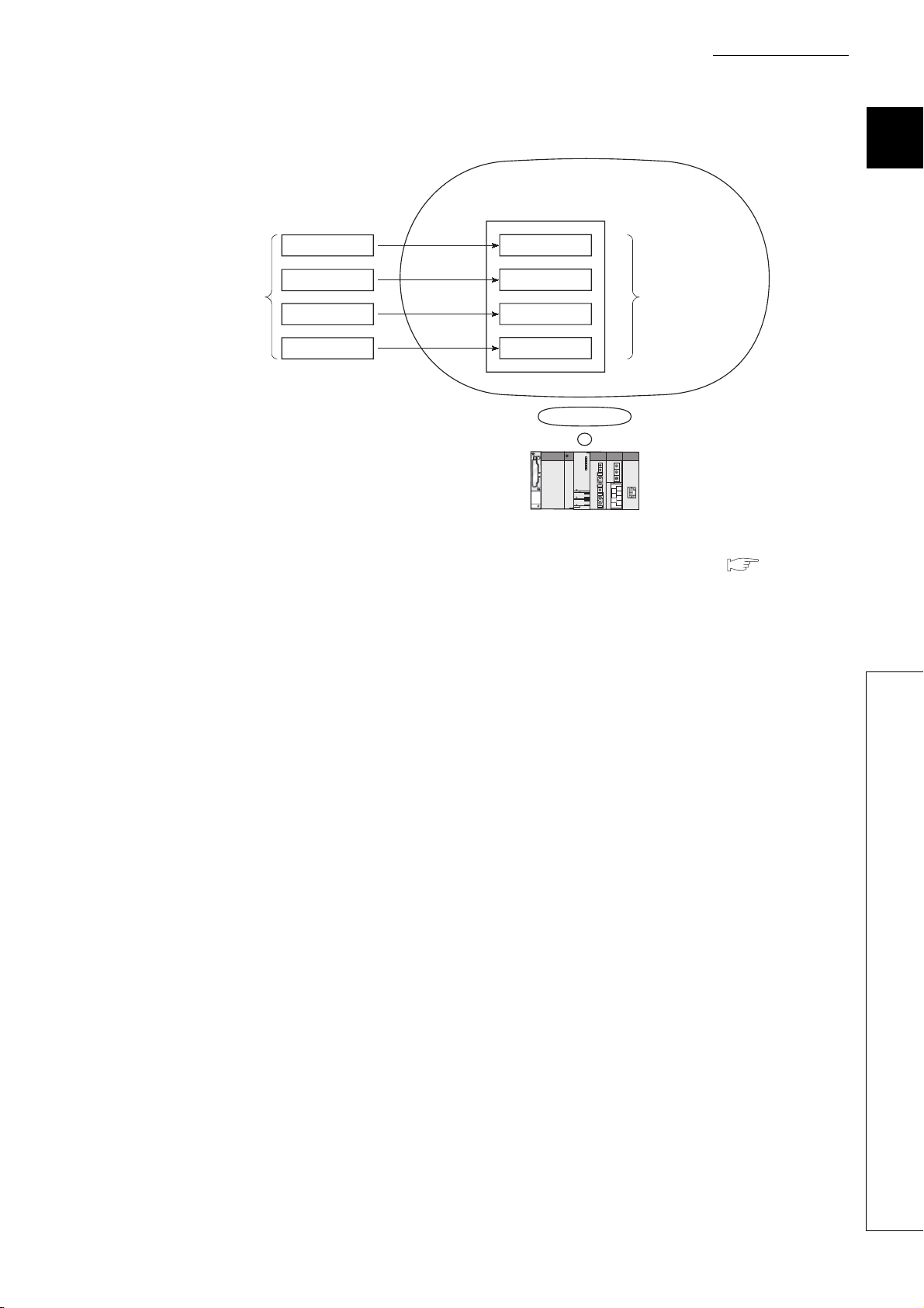
INTRODUCTION
This manual describes the memory maps, functions, programs, I/O number assignment, and devices of the Universal model
QCPU.
Before using this product, please read this manual and the relevant manuals carefully and develop familiarity with the
functions and performance of the Q series programmable controller to handle the product correctly.
Relevant CPU module
CPU module Model
Q00UJCPU, Q00UCPU, Q01UCPU, Q02UCPU, Q03UD(E)CPU,
Universal model QCPU
Remark
This manual does not describe the specifications of the power supply modules, base units, extension cables, memory
cards, and batteries.
For details, refer to the following.
QCPU User's Manual (Hardware Design, Maintenance and Inspection)
Q04UD(E)HCPU, Q06UD(E)HCPU, Q10UD(E)HCPU,
Q13UD(E)HCPU, Q20UD(E)HCPU, Q26UD(E)HCPU
For multiple CPU systems, refer to the following.
QCPU User's Manual (Multiple CPU System)
A - 11
Page 14

CONTENTS
CONTENTS
SAFETY PRECAUTIONS......................................................................................................................A - 1
CONDITIONS OF USE FOR THE PRODUCT ......................................................................................A - 9
REVISIONS ...........................................................................................................................................A - 10
INTRODUCTION ...................................................................................................................................A - 11
MANUALS .............................................................................................................................................A - 18
MANUAL PAGE ORGANIZATION .........................................................................................................A - 20
GENERIC TERMS AND ABBREVIATIONS ..........................................................................................A - 21
CHAPTER1 OVERVIEW 1-1 to 1-14
1.1 Processing Order in the CPU Module....................................................................................1 - 1
1.2 Storing and Executing Programs ...........................................................................................1 - 2
1.3 Structured Programming........................................................................................................1 - 3
1.4 Devices and Instructions Useful for Programming.................................................................1 - 6
1.5 Features.................................................................................................................................1 - 11
1.6 Checking Serial Number and Function Version .....................................................................1 - 13
CHAPTER2 SEQUENCE PROGRAMS 2-1 to 2-43
2.1 Sequence Program Overview................................................................................................2 - 1
2.2 Sequence Program Configuration..........................................................................................2 - 3
2.2.1 Main routine program........................................................................................................2 - 4
2.2.2 Subroutine program ..........................................................................................................2 - 5
2.2.3 Interrupt program ..............................................................................................................2 - 6
2.3 Settings When Program is Divided ........................................................................................2 - 13
2.3.1 Initial execution type program ...........................................................................................2 - 17
2.3.2 Scan execution type program ...........................................................................................2 - 20
2.3.3 Stand-by type program......................................................................................................2 - 21
2.3.4 Fixed scan execution type program ..................................................................................2 - 26
2.3.5 Changing the program execution type ..............................................................................2 - 30
2.4 Data Used in Sequence Programs ........................................................................................2 - 32
2.4.1 BIN (Binary Code) .............................................................................................................2 - 35
2.4.2 HEX (Hexadecimal)...........................................................................................................2 - 37
2.4.3 BCD (Binary-coded Decimal) ............................................................................................2 - 38
2.4.4 Real number (Floating-point data).....................................................................................2 - 39
2.4.5 Character string data.........................................................................................................2 - 43
CHAPTER3 CPU MODULE OPERATION 3-1 to 3-14
3.1 Initial Processing....................................................................................................................3 - 1
3.2 I/O Refresh (Refresh Processing with Input/Output Modules)...............................................3 - 2
3.3 Program Operation ................................................................................................................3 - 2
3.4 END Processing.....................................................................................................................3 - 2
3.5 Operation Processing in the RUN,STOP, or PAUSE Status ..................................................3 - 3
3.6 Operation Processing during Momentary Power Failure.......................................................3 - 5
3.7 Data Clear Processing...........................................................................................................3 - 6
A - 12
Page 15

3.8 I/O Processing and Response Delay.....................................................................................3 - 8
3.8.1 Refresh mode....................................................................................................................3 - 9
3.8.2 Direct mode.......................................................................................................................3 - 12
CHAPTER4 ASSIGNMENT OF BASE UNIT AND I/O NUMBER 4-1 to 4-17
4.1 Base Unit Assignment............................................................................................................ 4 - 1
4.1.1 Base mode........................................................................................................................4 - 1
4.1.2 Base unit assignment setting ............................................................................................4 - 2
4.2 I/O Number Assignment.........................................................................................................4 - 4
4.2.1 Concept of I/O number assignment ..................................................................................4 - 5
4.2.2 Setting I/O numbers ..........................................................................................................4 - 8
4.2.3 I/O number setting example ..............................................................................................4 - 13
4.2.4 Checking I/O numbers ......................................................................................................4 - 17
CHAPTER5 MEMORIES AND FILES USED FOR CPU MODULE 5-1 to 5-38
5.1 Memories Used for CPU Module ...........................................................................................5 - 1
5.1.1 Memory composition and storable data ............................................................................5 - 1
5.1.2 Program memory ..............................................................................................................5 - 5
5.1.3 Program cache memory....................................................................................................5 - 8
5.1.4 Standard ROM ..................................................................................................................5 - 11
5.1.5 Standard RAM...................................................................................................................5 - 12
5.1.6 Memory card .....................................................................................................................5 - 14
5.1.7 Writing to the Flash card by GX Developer .......................................................................5 - 18
5.1.8 Operating the program in the memory card (boot operation) ............................................5 - 23
5.1.9 Details of written files ........................................................................................................5 - 27
5.1.10 Specifying valid parameters (parameter-valid drive setting)..............................................5 - 28
5.2 Program File Structure...........................................................................................................5 - 30
5.3 File Operations by GX Developer and Handling Precautions................................................5 - 32
5.3.1 File operations...................................................................................................................5 - 32
5.3.2 Precautions for handling files ............................................................................................5 - 33
5.3.3 File size.............................................................................................................................5 - 34
5.3.4 Units of file sizes ...............................................................................................................5 - 36
CHAPTER6 FUNCTIONS 6-1 to 6-165
6.1 Function List...........................................................................................................................6 - 1
6.2 Constant Scan ....................................................................................................................... 6 - 4
6.3 Latch Function .......................................................................................................................6 - 7
6.4 Output Mode at Operating Status Change (STOP to RUN)...................................................6 - 10
6.5 Clock Function .......................................................................................................................6 - 13
6.6 Remote Operation.................................................................................................................. 6 - 18
6.6.1 Remote RUN/STOP..........................................................................................................6 - 18
6.6.2 Remote PAUSE.................................................................................................................6 - 21
6.6.3 Remote RESET.................................................................................................................6 - 23
A - 13
Page 16

6.6.4 Remote latch clear ............................................................................................................6 - 25
6.6.5 Relationship between remote operation and RUN/STOP status of the CPU module .......6 - 26
6.7 Q Series-compatible Module Input Response Time Selection (I/O Response Time) ............6 - 27
6.8 Error Time Output Mode Setting ............................................................................................6 - 29
6.9 H/W Error Time PLC Operation Mode Setting.......................................................................6 - 30
6.10 Intelligent Function Module Switch Setting ............................................................................6 - 31
6.11 Monitor Function ....................................................................................................................6 - 33
6.11.1 Monitor condition setting ...................................................................................................6 - 34
6.11.2 Local device monitor/test ..................................................................................................6 - 40
6.11.3 External input/output forced on/off ....................................................................................6 - 43
6.11.4 Executional conditioned device test ..................................................................................6 - 48
6.12 Writing Programs While CPU Module is in RUN Status.........................................................6 - 58
6.12.1 Online change (ladder mode)............................................................................................6 - 58
6.12.2 Online change (files) .........................................................................................................6 - 61
6.12.3 Precautions for online change...........................................................................................6 - 63
6.13 Execution Time Measurement ...............................................................................................6 - 69
6.13.1 Program monitor list ..........................................................................................................6 - 69
6.13.2 Interrupt program monitor list............................................................................................6 - 72
6.13.3 Scan time measurement ...................................................................................................6 - 73
6.14 Sampling Trace Function.......................................................................................................6 - 77
6.15 Debug Function from Multiple GX Developers....................................................................... 6 - 91
6.15.1 Simultaneous monitoring from multiple GX Developers function ......................................6 - 91
6.15.2 Online change function from multiple GX Developers ......................................................6 - 93
6.16 Watchdog Timer (WDT) .........................................................................................................6 - 95
6.17 Self-diagnostic Function.........................................................................................................6 - 97
6.17.1 LEDs indicating errors.......................................................................................................6 - 104
6.17.2 Error clear .........................................................................................................................6 - 104
6.18 Error History...........................................................................................................................6 - 105
6.19 System Protection..................................................................................................................6 - 106
6.19.1 Password registration........................................................................................................6 - 106
6.19.2 Remote password .............................................................................................................6 - 108
6.20 System Display of CPU Module with GX Developer..............................................................6 - 113
6.21 LED Indication........................................................................................................................ 6 - 116
6.21.1 Methods for turning off the LEDs.......................................................................................6 - 116
6.21.2 LED indication priority .......................................................................................................6 - 117
6.22 Interrupt from Intelligent Function Module .............................................................................6 - 119
6.23 Serial Communication Function .............................................................................................6 - 120
6.24 Service Processing ................................................................................................................6 - 128
6.24.1 Service processing setting ................................................................................................6 - 128
6.25 Initial Device Value.................................................................................................................6 - 135
6.26 Battery Life-prolonging Function............................................................................................6 - 139
6.27 Memory Check Function ........................................................................................................6 - 140
6.28 Latch Data Backup to Standard ROM Function .....................................................................6 - 141
6.29 Writing/Reading Device Data to/from Standard ROM ............................................................6 - 146
6.30 CPU Module Change Function with Memory Card................................................................6 - 147
6.30.1 Backup function to memory card.......................................................................................6 - 149
A - 14
Page 17

6.30.2 Backup data restoration function.......................................................................................6 - 157
6.31 Module model name read ......................................................................................................6 - 161
6.32 Module error collection...........................................................................................................6 - 162
CHAPTER7 COMMUNICATIONS WITH INTELLIGENT FUNCTION
MODULE 7-1 to 7-9
7.1 Communications between CPU Module and Intelligent Function Module .............................7 - 1
7.1.1 Initial setting and auto refresh setting by GX Configurator................................................7 - 2
7.1.2 Initial setting by initial device value ...................................................................................7 - 5
7.1.3 Communications with the FROM and TO instructions ......................................................7 - 5
7.1.4 Communications using the intelligent function module device..........................................7 - 6
7.1.5 Communications using the intelligent function module dedicated instruction ...................7 - 8
CHAPTER8 PARAMETERS 8-1 to 8-26
8.1 PLC Parameters .................................................................................................................... 8 - 2
8.2 Network Parameters ..............................................................................................................8 - 21
8.3 Remote Password.................................................................................................................. 8 - 26
CHAPTER9 DEVICES 9-1 to 9-94
9.1 Device List .............................................................................................................................9 - 1
9.2 Internal User Device ..............................................................................................................9 - 3
9.2.1 Input (X) ............................................................................................................................9 - 6
9.2.2 Output (Y)..........................................................................................................................9 - 8
9.2.3 Internal relay (M)...............................................................................................................9 - 9
9.2.4 Latch relay (L) ...................................................................................................................9 - 10
9.2.5 Annunciator (F) .................................................................................................................9 - 11
9.2.6 Edge relay (V) ...................................................................................................................9 - 15
9.2.7 Link relay (B).....................................................................................................................9 - 16
9.2.8 Link special relay (SB) ......................................................................................................9 - 18
9.2.9 Step relay (S) ....................................................................................................................9 - 19
9.2.10 Timer (T)............................................................................................................................9 - 20
9.2.11 Counter (C) .......................................................................................................................9 - 27
9.2.12 Data register (D)................................................................................................................9 - 31
9.2.13 Link register (W)................................................................................................................9 - 32
9.2.14 Link special register (SW) .................................................................................................9 - 34
9.3 Internal System Devices ........................................................................................................9 - 35
9.3.1 Function devices (FX, FY, FD) ..........................................................................................9 - 35
9.3.2 Special relay (SM) .............................................................................................................9 - 38
9.3.3 Special register (SD) .........................................................................................................9 - 39
9.4 Link Direct Device (J\)............................................................................................................ 9 - 40
9.5 Module Access Devices......................................................................................................... 9 - 43
9.5.1 Intelligent function module device (U\G) ...........................................................................9 - 43
9.5.2 Cyclic transmission area device (U3En\G)........................................................................9 - 45
A - 15
Page 18

9.6 Index Register (Z)/Standard Device Resister (Z) ...................................................................9 - 46
9.6.1 Index register (Z) ...............................................................................................................9 - 46
9.6.2 Standard device register (Z)..............................................................................................9 - 48
9.6.3 Switching from the scan execution type program to the interrupt/fixed scan execution
type program
9.7 File Register (R).....................................................................................................................9 - 53
9.7.1 File register data storage location.....................................................................................9 - 54
9.7.2 File register size................................................................................................................9 - 54
9.7.3 Differences in available accesses by storage memory .....................................................9 - 55
9.7.4 Registration procedure for the file register ........................................................................9 - 56
9.7.5 Specification methods of the file register...........................................................................9 - 61
9.7.6 Precautions for using the file register................................................................................9 - 62
9.8 Extended Data Register (D) and Extended Link Register (W)...............................................9 - 64
9.9 Nesting (N)............................................................................................................................ 9 - 70
9.10 Pointer (P)..............................................................................................................................9 - 71
9.10.1 Local pointer..................................................................................................................... 9 - 72
9.10.2 Common pointer................................................................................................................9 - 74
9.11 Interrupt Pointer(I)..................................................................................................................9 - 76
9.11.1 List of interrupt pointer numbers and interrupt factors ......................................................9 - 77
9.12 Other Devices ........................................................................................................................9 - 78
9.12.1 SFC block device (BL) ......................................................................................................9 - 78
9.12.2 Network No. specification device (J) .................................................................................9 - 78
9.12.3 I/O No. specification device (U).........................................................................................9 - 79
9.12.4 Macro instruction argument device (VD)...........................................................................9 - 80
9.13 Constants...............................................................................................................................9 - 81
9.13.1 Decimal constant (K).........................................................................................................9 - 81
9.13.2 Hexadecimal constant (H) .................................................................................................9 - 81
9.13.3 Real number (E)................................................................................................................9 - 82
9.13.4 Character string (" ")..........................................................................................................9 - 83
9.14 Convenient Usage of Devices................................................................................................9 - 84
9.14.1 Global device ....................................................................................................................9 - 84
9.14.2 Local device ......................................................................................................................9 - 85
....................................................................................................9 - 49
CHAPTER10 CPU MODULE PROCESSING TIME 10-1 to 10-18
10.1 Scan Time..............................................................................................................................10 - 1
10.1.1 Scan time structure ...........................................................................................................10 - 1
10.1.2 Time required for each processing included in scan time .................................................10 - 2
10.1.3 Factors that increase the scan time ..................................................................................10 - 11
CHAPTER11 PROCEDURES FOR WRITING PROGRAM TO CPU
MODULE 11-1 to 11-10
11.1 Items to be Considered for Creating Programs .....................................................................11 - 1
11.2 Hardware Check ....................................................................................................................11 - 3
11.3 Procedure for Writing One Program ......................................................................................11 - 5
A - 16
Page 19

11.4 Procedure for Writing Multiple Programs...............................................................................11 - 7
11.5 Procedure for Boot Operation................................................................................................11 - 10
CHAPTER12 SPECIAL RELAY LIST AND SPECIAL REGISTER LIST 12-1 to 12-78
12.1 SPECIAL RELAY LIST...........................................................................................................12 - 1
12.2 SPECIAL REGISTER LIST....................................................................................................12 - 27
APPENDICES App-1 to App-72
Appendix 1 List of Parameter Numbers.........................................................................................App- 1
Appendix 2 Functions Added or Changed by Version Upgrade.....................................................App- 6
Appendix 3 Method of Replacing Basic Model QCPU or High Performance Model QCPU
with Universal Model QCPU
Appendix 3.1 Replacement Precautions ........................................................................... App- 8
Appendix 3.1.1 Replacing Basic model QCPU with Universal model QCPU ....................... App- 8
Appendix 3.1.2 Replacing High Performance model QCPU with Universal model QCPU ......App- 12
Appendix 3.2 Applicable devices and software .................................................................. App- 19
Appendix 3.3 Instructions ..............................................................................................App- 23
Appendix 3.3.1 Instructions not supported in the Universal model QCPU and replacing
methods
Appendix 3.3.2 Replacing programs using multiple CPU transmission dedicated
instructions
Appendix 3.3.3 Program replacement examples ...........................................................App- 26
Appendix 3.4 Functions.................................................................................................App- 40
Appendix 3.4.1 Floating-point operation instructions ......................................................App- 40
Appendix 3.4.2 Error check processing for floating-point data comparison instructions .........App- 48
Appendix 3.4.3 Range check processing for index-modified devices ................................. App- 52
Appendix 3.4.4 Device latch function ..........................................................................App- 55
Appendix 3.4.5 File usability setting............................................................................App- 57
Appendix 3.4.6 Parameter-valid drive and boot file setting .............................................. App- 60
Appendix 3.4.7 External input/output forced on/off function ............................................. App- 63
Appendix 3.5 Special Relay and Special Register............................................................... App- 67
Appendix 3.5.1 Special relay list ................................................................................App- 67
Appendix 3.5.2 Special register list............................................................................. App- 70
Appendix 4 Device Point Assignment Sheet..................................................................................App- 72
...............................................................................App- 8
..........................................................................................App- 23
......................................................................................App- 25
INDEX Index-1 to Index-4
A - 17
Page 20

MANUALS
To understand the main specifications, functions, and usage of the CPU module, refer to the basic manuals.
Read other manuals as well when using a different type of CPU module and its functions.
Order each manual as needed, referring to the following list.
:Basic manual, :Other CPU module manuals
Manual name
< Manual number (model code) >
User's manual
QCPU User's Manual (Hardware Design,
Maintenance and Inspection)
< SH-080483ENG (13JR73) >
QnUCPU User's Manual (Function
Explanation, Program Fundamentals)
< SH-080807ENG (13JZ27) >
QCPU User's Manual (Multiple CPU System)
< SH-080485ENG (13JR75) >
QnUCPU User's Manual (Communication via
Built-in Ethernet Port)
< SH-080811ENG (13JZ29) >
Programming manual
QCPU Programming Manual (Common
Instructions)
< SH-080809ENG (13JW10) >
QCPU (Q Mode)/QnACPU Programming
Manual (SFC)
< SH-080041 (13JF60) >
QCPU (Q Mode) Programming Manual
(MELSAP-L)
< SH-080076 (13JF61) >
QCPU (Q Mode) Programming Manual
(Structured Text)
< SH-080366E (13JF68) >
QCPU (Q Mode) / QnACPU Programming
Manual (PID Control Instructions)
< SH-080040 (13JF59) >
Specifications of the hardware (CPU modules, power
supply modules, base units, extension cables, and
memory cards), system maintenance and inspection,
troubleshooting, and error codes
Functions, methods, and devices for programming
Information on multiple CPU system configuration
(system configuration, I/O numbers, communication
between CPU modules, and communication with the
input/output modules and intelligent function
modules)
Functions for the communication via built-in Ethernet
port of the CPU module
How to use sequence instructions, basic instructions,
and application instructions
System configuration, performance specifications,
functions, programming, debugging, and error codes
for SFC (MELSAP3) programs
Programming methods, specifications, and functions
for SFC (MELSAP-L) programs
Programming methods using structured languages
Dedicated instructions for PID control
Description Manual type
A - 18
Page 21

Other relevant manuals
Manual name Description
CC-Link IE Controller Network Reference
Manual
< SH-080668ENG (13JV16) >
Q Corresponding MELSECNET/H Network
System Reference Manual (PLC to PLC
network)
< SH-080049 (13JF92) >
Q Corresponding MELSECNET/H Network
System Reference Manual (Remote I/O
network)
< SH-080124 (13JF96) >
Q Corresponding Ethernet Interface Module
User's Manual (Basic)
< SH-080009 (13JL88) >
Q Corresponding Ethernet Interface Module
User's Manual (Application)
< SH-080010 (13JL89) >
CC-Link System Master/Local Module User's
Manual
< SH-080394E (13JR64) >
Q Corresponding Serial Communication
Module User's Manual (Basic)
< SH-080006 (13JL86) >
Q Corresponding Serial Communication
Module User's Manual (Application)
< SH-080007 (13JL87) >
Q Corresponding MELSEC Communication
Protocol Reference Manual
< SH-080008 (13JF89) >
GX Developer Version 8 Operating Manual
< SH-080373E (13JU41) >
Specifications, procedures and settings before system operation, parameter
setting, programming, and troubleshooting of the CC-Link IE controller
network module
Specifications, procedures and settings before system operation, parameter
setting, programming, and troubleshooting of a MELSECNET/H network
system (PLC to PLC network)
Specifications, procedures and settings before system operation, parameter
setting, programming, and troubleshooting of a MELSECNET/H network
system (remote I/O network)
Specifications, procedures for data communication with external devices,
line connection (open/close), fixed buffer communication, random access
buffer communication, and troubleshooting of the Ethernet module
E-mail function, programmable controller CPU status monitoring function,
communication via MELSECNET/H or MELSECNET/10, communication
using the data link instructions, and file transfer function (FTP server) of the
Ethernet module
System configuration, performance specifications, functions, handling,
wiring, and troubleshooting of the QJ61BT11N
Overview, system configuration, specifications, procedures before
operation, basic data communication method with external devices,
maintenance and inspection, and troubleshooting for using the serial
communication module
Special functions (specifications, usage, and settings and data
communication method with external devices of the serial communication
module
Communication method using the MC protocol, which reads/writes data to/
from the CPU module via the serial communication module or Ethernet
module
Operating methods of GX Developer, such as programming and printout
A - 19
Page 22
MANUAL PAGE ORGANIZATION
The detailed explanation of "Note . " is
provided under the corresponding
"Note . " at the bottom of the page.
ReferenceNote (icon)
The section in this manual or
another relevant manual that can
be referred to is shown with .
Chapter
The chapter of the current page can be
easily identified by this indication on the
right side.
Note (detailed explanation)
The detailed note corresponding to each icon
is described.
Section title
The section number and title of the current
page can be easily identified.
* cining page components, and differs from an actual page.
Icons
Universal model QCPU
Universal
Icons indicate that specifications described on the page
contain some precautions.
Description
In addition, this manual uses the following types of explanations.
In addition to description of the page, notes or functions that require special attention are described here.
Remark
The reference related to the page or useful information are described here.
A - 20
Page 23
GENERIC TERMS AND ABBREVIATIONS
Unless otherwise specified, this manual uses the following generic terms and abbreviations.
* indicates a part of the model or version.
(Example): Q33B, Q35B, Q38B, Q312B
Generic term/abbreviation Description
Series
Q series Abbreviation for Mitsubishi MELSEC-Q series programmable controller
CPU module type
CPU module Generic term for the Universal model QCPU
Universal model QCPU
Built-in Ethernet port QCPU
Motion CPU
PC CPU module
C Controller module
CPU module model
QnUD(H)CPU
Base unit type
Base unit
Main base unit
Extension base unit
Slim type main base unit
Redundant power main base unit
Redundant power extension base
unit
Multiple CPU high speed main base
unit
Base unit model
Q3 B
Q3 SB
Q3 RB
Q3 DB
Q5 B
Q6 B
Q6 RB
Q3 B
Generic term for the Q00UJCPU, Q00UCPU, Q01UCPU, Q02UCPU,
Q03UDCPU, Q04UDHCPU, Q06UDHCPU, Q10UDHCPU, Q13UDHCPU,
Q20UDHCPU, Q26UDHCPU, Q03UDECPU, Q04UDEHCPU, Q06UDEHCPU,
Q10UDEHCPU, Q13UDEHCPU, Q20UDEHCPU, and Q26UDEHCPU
Generic term for the Q03UDECPU, Q04UDEHCPU, Q06UDEHCPU,
Q10UDEHCPU, Q13UDEHCPU, Q20UDEHCPU, and Q26UDEHCPU
Generic term for Mitsubishi motion controllers, Q172CPUN, Q173CPUN,
Q172HCPU, Q173HCPU, Q172CPUN-T, Q173CPUN-T, Q172HCPU-T,
Q173HCPU-T, Q172DCPU, and Q173DCPU
Generic term for MELSEC-Q series PC CPU module, PPC-CPU852(MS)-512,
manufactured by CONTEC Co., Ltd.
Generic term for the Q06CCPU-V-H01, Q06CCPU-V, Q06CCPU-V-B, and
Q12DCCPU-V C Controller modules
Generic term for the Q03UDCPU, Q04UDHCPU, Q06UDHCPU, Q10UDHCPU,
Q13UDHCPU, Q20UDHCPU, and Q26UDHCPU
Generic term for the main base unit, extension base unit, slim type main base
unit, redundant power main base unit, redundant power extension base unit, and
multiple CPU high speed main base unit
Generic term for the Q3 B, Q3 SB, Q3 RB, and Q3 DB
Generic term for the Q5 B, Q6 B, and Q6 RB
Another name for the Q3 SB
Another name for the Q3 RB
Another name for the Q6 RB
Another name for the Q3 DB
Generic term for the Q33B, Q35B, Q38B, and Q312B main base units
Generic term for the Q32SB, Q33SB, and Q35SB slim type main base units
Another name for the Q38RB main base unit for redundant power supply system
Generic term for the Q38DB and Q312DB multiple CPU high speed main base
units
Generic term for the Q52B and Q55B extension base units
Generic term for the Q63B, Q65B, Q68B, and Q612B extension base units
Another name for the Q68RB extension base unit for redundant power supply
system
A - 21
Page 24

Generic term/abbreviation Description
Power supply module
Power supply module
Q series power supply module
Slim type power supply module Abbreviation for the Q61SP slim type power supply module
Redundant power supply module
Network
MELSECNET/H Abbreviation for the MELSECNET/H network system
Ethernet Abbreviation for the Ethernet network system
CC-Link Abbreviation for the Control & Communication Link
Memory card
Memory card Generic term for the SRAM card, Flash card, and ATA card
SRAM card
Flash card Generic term for the Q2MEM-2MBF and Q2MEM-4MBF Flash cards
ATA car d
Others
Generic term for the Q series power supply module, slim type power supply
module, and redundant power supply module
Generic term for the Q61P-A1, Q61P-A2, Q61P, Q61P-D, Q62P, Q63P, Q64P, and
Q64PN power supply modules
Generic term for the Q63RP and Q64RP power supply modules for redundant
power supply
Generic term for the Q2MEM-1MBS, Q2MEM-2MBS, Q3MEM-4MBS, and
Q3MEM-8MBS SRAM cards
Generic term for the Q2MEM-8MBA, Q2MEM-16MBA, and Q2MEM-32MBA ATA
cards
GX Developer
Extension cable
Battery
GOT
Product name for SW D5C-GPPW-E GPP function software package compatible
with the Q series
Generic term for the QC05B, QC06B, QC12B, QC30B, QC50B, and QC100B
extension cables
Generic term for the Q6BAT, Q7BAT, and Q8BAT CPU module batteries,
Q2MEM-BAT SRAM card battery, and Q3MEM-BAT SRAM card battery
Generic term for Mitsubishi Graphic Operation Terminal, GOT-A*** series, GOT-F***
series, and GOT1000 series
A - 22
Page 25
CHAPTER1 OVERVIEW
CHAPTER1 OVERVIEW
The CPU module performs sequence control by executing programs.
This chapter describes the processing order in the CPU module, locations where the created programs are stored, and
devices and instructions useful for programming.
1.1 Processing Order in the CPU Module
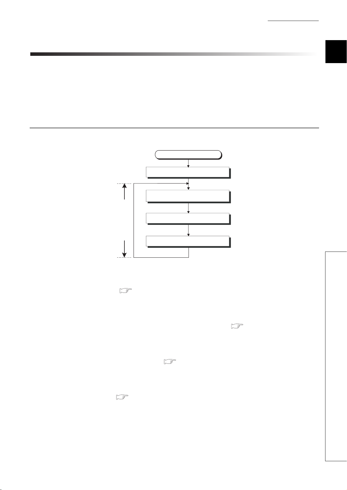
The CPU module performs processing in the following order.
Power-on or reset
Initial processing
Refresh processing with
input/output modules
1
2
3
4
5
6
7
Program operation processing
Scan time
END processing
Figure 1.1 Processing order in the CPU module
(1) Initial processing ( Section 3.1)
The CPU module performs preprocessing required for program operations.
The preprocessing is performed only once when the module is powered on or reset.
(2) Refresh processing with input and output modules ( Section 3.2)
The CPU module takes on/off data from the input module or intelligent function module and outputs on/off data to
the output module or intelligent function module.
(3) Program operation processing ( Section 3.3)
The CPU module sequentially executes the program stored in the module from the step 0 to the END or FEND
instruction.
8
1.1 Processing Order in the CPU Module
(4) END processing ( Section 3.4)
The CPU module performs refresh processing with network modules or communicates with external devices.
1 - 1
Page 26
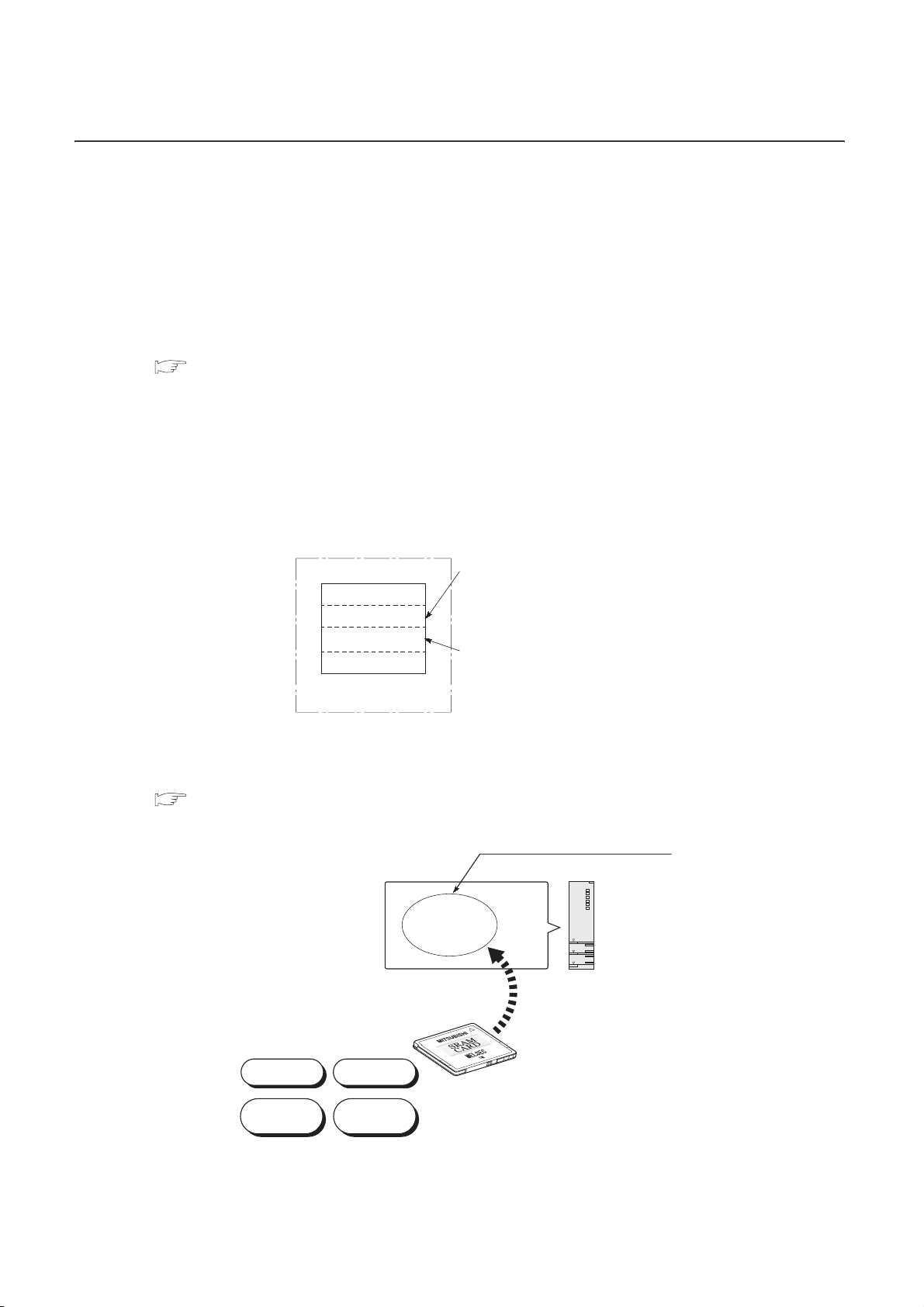
1.2 Storing and Executing Programs
This section describes where to store and how to execute the programs in the CPU module.
(1) Programming
Programs are created with GX Developer.
For details of program configuration and execution conditions, refer to CHAPTER 2.
(2) Storing programs
Created programs and set parameters are stored in the following memories of the CPU module.
( Section 5.1)
• Program memory
• Standard ROM (parameters only)
• Memory card
(3) Executing programs
The CPU module executes the programs stored in the program memory.
CPU module
Program memory
Parameter
Program
Device comment
Initial device value
The CPU module executes
the programs stored here.
Comments are stored
separately from the program.
Figure 1.2 Executing programs
To execute the programs stored in a memory card, the programs need to be booted to the program memory
( Section 5.1.8) when the CPU module is powered off and then on or reset.
The CPU module executes the programs
booted from a memory card to here.
Program
memory
CPU moduleBoot
Parameter Program
Memory card
Device
comment
Initial device
value
Figure 1.3 Executing programs stored in a memory card
1 - 2
Page 27
CHAPTER1 OVERVIEW
1.3 Structured Programming
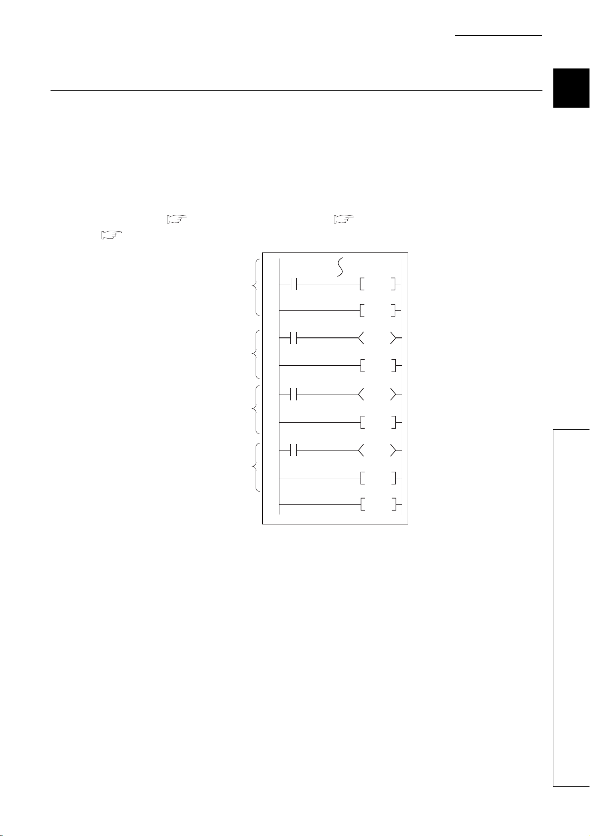
The programs to be executed in the CPU module can be structured in the following two ways.
• In one program
• By dividing into multiple files
(1) Structuring in one program
Structured programming is available by creating one program as a collection of three program sections: main
routine program ( Section 2.2.1), subroutine program ( Section 2.2.2), and interrupt program
( Section 2.2.3).
Main routine
program
P1
Subroutine
program 1
CALL P1
FEND
Y10
RET
1
2
3
4
5
6
7
Subroutine
program 2
Interrupt program
Figure 1.4 Structuring in one program
P8
I0
Y11
RET
Y12
IRET
END
8
1.3 Structured Programming
1 - 3
Page 28
(2) Structuring by dividing into multiple files
A program is stored in a file.
Changing the file name allows the CPU module to store multiple programs.
Multiple programs can be stored
by changing the file name.
File name: PARAM
Parameter Program Program
GX Developer
Figure 1.5 Structuring by dividing into multiple files
Dividing into multiple files according to the processes or functions enables simultaneous programming by two or
more designers. Managing the files separately eases reuse and utilization to other programs.
Structured programming is efficient in this way because only the corresponding file needs to be modified or
debugged in case of change in the specifications.
File name: ABC File name: ABC File name: DEF
Device
comment
CPU module
(a) Dividing into multiple files according to the processes
Program memory/memory card
Program ACarrying in
Manufacturing
Processing contents
are divided according
to the processes.
*1: The processing contents divided according to the processes can further be divided and managed according to the
functions.
*2: The execution order can be set in the Program tab of the PLC parameter dialog box. ( Section 2.3(2)).
Assembly
Carrying out
Figure 1.6 Dividing into multiple files according to the processes
Program B
Program C
Program D
*1
Program A to D will
be executed in the
specified order. *2
1 - 4
Page 29
CHAPTER1 OVERVIEW
(b) Dividing into multiple files according to the functions
Program memory/memory card
Initial processing
Main processing
Processing contents
are divided according
to the functions.
*1: The execution order and conditions can be set in the Program tab of the PLC parameter dialog box. ( Section 2.3(2)).
Communication
processing
Error processing
Figure 1.7 Dividing into multiple files according to the functions
Program A
Program B
Program C
Program D
The execution order and
conditions for program
A to D can be set. *1
1
2
3
4
5
6
7
8
1.3 Structured Programming
1 - 5
Page 30
1.4 Devices and Instructions Useful for Programming
The CPU module is provided with devices and instructions useful for programming.
This section describes the outline of these devices and instructions.
(1) Various ways of device specification
(a) Using each bit of a word device as a contact or coil
By specifying a bit of a word device, the bit can be used as a contact or coil.
X0
SET D0.5
D0.5
SET Y10
Figure 1.8 Specifying a bit of a word device
A bit-specified word device (turns on
(switches to 1) the 5th bit (b5) of D0.)
A bit-specified word device (turns on/off depending
on the on/off (1/0) status of the 5th bit (b5) of D0.)
(b) Easy direct processing in units of one point
Use of the direct access input (DX ) and direct access output (DY ) enables easy direct processing (in units
of one point) in the program. ( Section 3.8.2)
M0 DX10
Direct access input
DY100
On/off data is output to the
output module when the
instruction is executed.
On/off data is input from
the input module when the
instruction is executed.
1 - 6
Figure 1.9 Direct processing in units of one point
(c) No input pulse conversion required by using a differential contact
Pulse conversion processing for inputs is no longer required with the use of a differential contacts ( and
).
X0
Y100
X1
Differential contact
Y100
Figure 1.10 Use of a differential contact
On at the rising
edge of X0
X0
M0
Y100
X1
PLS
M0
Y100
Page 31
CHAPTER1 OVERVIEW
(d) Direct access to the buffer memory of the intelligent function module
The buffer memory of the intelligent function module can be used as a device area in a program.
( Section 9.5.1)
X0
+P
Power supply module
CPU module
Input module (16 points)
Figure 1.11 Direct access to the buffer memory of the intelligent function module
*1
D0U4\G12
The CPU module can read the
data in the buffer memory
address 12 of the Q64AD.
*1:U4\G12
Input module (16 points)
Input module (16 points)
Q64AD (16 points)
Q64AD (16 points)
Q62AD (16 points)
Output module (16 points)
Output module (16 points)
I/O number: X/Y40 to X/Y4F
Specifying the buffer
memory address
Specifying the I/O number of
the intelligent function module
(e) Direct access to the link devices
The link devices (LX, LY, LB, LW, SB, or SW) in network modules can be directly accessed without
the refresh setting. (
M0
Section 9.4)
The CPU module can directly read the data in the
link register (LW12) of the number 5 network module.
J5\W12
D0
J5\W12+P
Specifying the
link register
Specifying the
network number
1
2
3
4
5
6
7
8
1.4 Devices and Instructions Useful for Programming
Power supply module
CPU module
Input module (16 points)
Input module (16 points)
Q68AD (16 points)
Q68AD (16 points)
Q62AD (16 points)
Output module (16 points)
QJ71LP21-25
Network number 5
Figure 1.12 Direct access to the link devices
Output module (16 points)
1 - 7
Page 32

(2) Structural description of programs
Use of the index register and edge relay enables easy structured programming including the pulse conversion
processing. ( Section 9.2.6)
X0Z0 X1Z0
FOR n
V0Z1
Y8Z2
X0 X1
M0
X10 X11
M10
Multiple number (n) of
PLS M0
Y8
PLS M10
Y18
similar programs can
be executed by one
description.
NEXT
X170 X171
M170
PLS M170
Y178
Figure 1.13 Structured programming including the pulse conversion processing
(3) Easy data processing
(a) Using real numbers and character string constants without conversion
Real numbers (floating-point data) and character string constants can be used without conversion for
programming.
X0
E+P E1.23
Real number addition instruction
D0
R0
Real number
data
E1.23
Real number
data
D0
E3.45 E4.68
D1
Real number
R0
R1
data
$+P D5 "CPU" D10
Character string data link instruction
Character
string data
D5
NULL
D6
"0" "Q"
"2"
*1
Character
string data
"CPU"
D10
D11
D12
D13
Character
string data
"0"
"Q"
"C"
"2"
"U"
"P"
NULL *1
Figure 1.14 Using real numbers and character string constants
*1: The NULL character represents "00H" (end of character strings).
(b) High-speed processing of bulk data
Extension of the data table operation instructions, such as the data table processing instruction, allows highspeed processing of bulk data.
X0
Device
where the
data is
currently
stored
Instruction for inserting data
Device
where
the data
is to be
stored
Insertion
position
D0
15
to the table
Figure 1.15 Data processing with the table processing instruction
K2R0D0FINSP
FIF0 table FIF0 table
R0
R1
R2
R3
3
10
20
30
R0
R1
R2
R3
R4
4
10
15
20
30R4
1 - 8
Page 33

CHAPTER1 OVERVIEW
(4) Flexible management of subroutine programs
(a) Subroutine program sharing
The number of steps in a program can be reduced by sharing subroutine programs.
In addition, creating and managing programs become easier.
Subroutine programs can be created within the same program and called. Subroutine programs in other
programs can also be called by using the common pointer.
Program C
Program A
M0
0
Program B
M10
0
P1000CALLP
Calling P1000
Calling P1000
P1000CALLP
Common pointer
Subroutine program
SM400
P1000
Always
on
M0
M0
MOV
1
2
3
4
K4X0MOV
R0
R0K4X20
5
6
RET
7
Figure 1.16 Subroutine program sharing
8
1.4 Devices and Instructions Useful for Programming
1 - 9
Page 34

(b) Subroutine call instruction with argument passing
Subroutine program that is called more than one time can be created easily.
Main routine program
Argument specification
M0
K4X0W0
R0
Argument from FD2
Argument to FD1
Argument to FD0
K4X10W10
R10
Argument from FD2
Argument to FD1
Argument to FD0
FEND
100
CALLP
CALLP
P0
Subroutine program
specification
Argument specification
P0
0
M10
*1
*1
Subroutine program
SM400
P0
Always
on
Figure 1.17 Calling subroutine program with argument passing
*1: For input and output conditions for an argument, refer to Section 9.3.1.
M0
M0
Source data
MOV
FD0MOV
FD2
FD2FD1
RET
END
Destination data
1 - 10
Page 35

CHAPTER1 OVERVIEW
1.5 Features
This section describes the features specific to the Universal model QCPU.
(1) High-speed processing more than ever
The processing time required for the basic instructions, floating-point operations, and accesses to the file register
becomes shorter than the existing Q series CPU modules.
*1
Use of a standard device register (Z)
instruction).
*1: An index register used between register operations is designated as a standard device register.( Section 9.6.2)
(2) Large-capacity file register
The file register whose capacity is 640K points at maximum (4086K points at maximum when a memory card is
*2
used)
can be set inside the CPU module.
*2: For the Q26UDHCPU and Q26UDEHCPU only
(3) Use of double-precision floating-point operation instructions
The double-precision floating-point operation instructions (64-bit instructions) are available as well as the existing
single-precision floating-point operation instructions. ( Section 2.4.4)
This enables more accurate analog control and positioning control.
achieves high-speed processing between register operations (transfer
1
2
3
4
5
6
7
8
(4) Using the file register area as the data register and link register
The file register (ZR) area can be used as an pseudo extended area*3 of the data register (D) and link register
(W). ( Section 9.8)
Programming using the extended data register (D) or extended link register (W) whose capacity is 640K points at
*4
maximum (4086K points at maximum when a memory card is used)
device.
*3: Extended areas of the data register (D) and link register (W) are called the extended data register (D) and extended link
register (W), respectively.
*4: For the Q26UDHCPU and Q26UDEHCPU only
W0.0
W10000.0
B80
MOV D0 W200
SET W100.0
MOV D30000 W10200
SET W10100.0
Internal user devices
are used.
The extended data
register (D) and
extended link register
(W) are used.
is available in addition to the internal user
GX Developer
1.5 Features
Figure 1.18 Extended data register (D) and extended link register (W)
1 - 11
Page 36

(5) 32-bit index modification
Since the index modification range is expanded to 32 bits, index modification for the entire file register areas is
possible. ( Section 9.6.1)
File register in the serial
number access method
ZR0
ZR1
ZR32767
ZR32768
ZR1042431
Applicable range
of existing index
modification
Applicable range of index modification
for the Universal model QCPU
Figure 1.19 32-bit index modification
SM400
K1042431 Z0DMOV
ZR0Z0 D0MOV
Use the index register (Z) when indexing the
file register (ZR) in the serial number access
method by 32 bits.
(6) Communication via the built-in Ethernet port of the CPU module
The Built-in Ethernet port QCPU can communicate with MELSOFT, GOT, and external devices using the built-in
Ethernet port of the module.
QnUCPU User's Manual (Communication via Built-in Ethernet Port)
(7) Communication with the personal computer and HMI by the serial
communication function ( Section 6.23)
The Q00UJCPU, Q00UCPU, Q01UCPU, and Q02UCPU can communicate using the MELSEC communication
protocol (hereafter, MC protocol) by connecting a RS-232 interface and personal computer or HMI.
RS-232 cable
Personal computer or HMI
Communication using the MC protocol
Figure 1.20 Communication with the personal computer or HMI
The CPU module functions are added at the update of serial number of CPU module or GX Developer version.
For functions added by the update, refer to Appendix 2.
1 - 12
Page 37

CHAPTER1 OVERVIEW
1.6 Checking Serial Number and Function Version
The serial number and function version of the CPU module can be checked on the rating plate, on the front of the
module, and on the System monitor screen in GX Developer.
(1) Checking on the rating plate
The rating plate is located on the side of the CPU module.
Serial number (first five digits)
Function version
Relevant regulation
standards
Figure 1.21 Rating plate
(2) Checking on the front of the module
The serial number on the rating plate is printed on the front (at the bottom) of the module. This applies only to the
CPU module manufactured in mid-September, 2007 or later.
1
2
3
4
5
6
7
8
Q03UDCPU
PULL
RS-232
MODE
RUN
ERR.
USER
BAT.
BOOT
USB
Serial number
Figure 1.22 Front of the module
1.6 Checking Serial Number and Function Version
1 - 13
Page 38

(3) Checking on the System monitor (Product Information List) screen
To open the screen for checking the serial number and function version, select [Diagnostics] [System monitor]
and click the button in GX Developer.
Product Inf. List...
On the same screen, the serial number and function version of intelligent function modules can also be checked.
Serial
number
Function
version
Product
number
Figure 1.23 System monitor (Product Information List) screen
[Serial number, function version, and product number]
• The serial number of the module is displayed in the "Serial No." column.
• The function version of the module is displayed in the "Ver." column.
• The serial number (product number) printed on the rating plate of the module is displayed in the "Product
No." column.
Note that "-" is displayed for the module that does not support the product number display.
The serial number displayed on the Product Information List screen of GX Developer may differ from that on the rating plate
and on the front of the module.
• The serial number on the rating plate and on the front of the module indicates the management information of the
product.
• The serial number displayed on the Product Information List screen indicates the functional information of the
product.
The functional information of the product will be updated when a function is added.
1 - 14
Page 39

CHAPTER2 SEQUENCE PROGRAMS
CHAPTER2 SEQUENCE PROGRAMS
2.1 Sequence Program Overview
(1) Definition
Sequence program is one of the programs that can be executed in the CPU module.
A sequence program consists of instructions, such as sequence instructions, basic instruction, and
application instruction.
X0
M0
T0
X1
BIN K4X10 D0
X41
FROM H5 K0 D10 K1
Figure 2.1 Sequence program
K100
T0
Y30
Sequence instruction
Basic instruction
Application instruction
1
2
3
4
5
6
7
Remark
For the instructions used in sequence programs, refer to the following.
QCPU Programming Manual (Common Instructions)
8
2.1 Sequence Program Overview
2 - 1
Page 40

(2) Programming method
There are two programming modes for sequence programs.
• Ladder mode
• List mode
(a) Ladder mode
Ladder mode is a mode based on the concept of sequential control by relay circuits.
A program in ladder mode is similar to a schematic for a set of relay circuits.
of ladder blocks is available.
A ladder block, which starts from the left rail and ends at the right rail, is the minimum unit for
operating sequence programs.
Programming in units
Left rail
Step number
N/O
contact
X0
0
X1 X2
2
X4 X5
8
Y24
* X0 to X5: Input, Y20 to Y24: Output
N/C
contact
X3
Figure 2.2 Ladder mode
Coil (output)
Y20
Y21
Y22
Y23
Y24
Right rail
Ladder block
(b) List mode
List mode uses dedicated instructions for programming. The symbols, such as contacts and coils,
used in ladder mode are replaced with dedicated instructions.
The following instructions are used for normally open contacts, normally closed contacts, and coils.
• Normally open contact ••• LD, AND, OR
• Normally closed contact ••• LDI, ANI, ORI
• Coil ••• OUT
2 - 2
Remark
There are two other types of programs that can be executed in the CPU module: SFC programs and ST
programs.
For details, refer to the following.
QCPU (Q Mode)/QnACPU Programming Manual (SFC)
QCPU (Q Mode) Programming Manual (MELSAP-L)
QCPU (Q Mode) Programming Manual (Structured Text)
Page 41

CHAPTER2 SEQUENCE PROGRAMS
(3) Sequence program operation
A sequence program is sequentially operated from the step 0 to the END or FEND instruction.
In ladder mode, a sequence program is operated from left to right and top to bottom in a ladder block.
[Ladder mode]
From left to right
From top
to bottom
1) 2)
X0 X1 X5 X6 X7
0
3)6)4)
X2
X4
10
* Program operations are executed in the
order of 1) to 11).
7) 8) 9)
X3
5)
Figure 2.3 Comparison between ladder mode and list mode
10)
Y10
11)
END
2.2 Sequence Program Configuration
Sequence programs are classified into the following three types.
Program
operations are
sequentially
executed from
the step 0 to the
END instruction.
[List mode]
0 LD X0
1 AND X1
2 LD X2
3 AND X3
4 ORB
5 OR X4
6 AND X5
7 AND X6
8 AND X7
9 OUT Y10
10 END
Step number
0)
1)
2)
3)
4)
5)
6)
7)
8)
9)
10)
11)
1
2
3
4
5
6
7
• Main routine program
• Subroutine program
• Interrupt program
File A
Main routine
program
FEND
P0
I0
Figure 2.4 Sequence program classification
Subroutine
program
RET
Interrupt
program
IRET
END
8
2.2 Sequence Program Configuration
2 - 3
Page 42

2.2.1 Main routine program
(1) Definition
Main routine program is an entire program from the step 0 to the END or FEND instruction.
(2) Program operation
A main routine program executes its operations from the step 0 to the END or FEND instruction and
then performs END processing.
After the END processing, the program restarts its operations from the step 0.
Step 0
Main routine
program
END/FEND
Figure 2.5 Main routine program
When multiple programs are executed, the main routine program operation after execution of the END or
FEND instruction varies depending on the preset execution conditions. ( Section 2.3.1)
END/FEND
END
processing
Indicates execution of
the program.
The program operation
returns to the step 0.
Remark
For details of the END and FEND instructions, refer to the following.
QCPU Programming Manual (Common Instructions)
2 - 4
Page 43

CHAPTER2 SEQUENCE PROGRAMS
2.2.2 Subroutine program
(1) Definition
Subroutine program is a program from a pointer (P ) to the RET instruction.
This program is executed only when it is called by a subroutine program call instruction (such as
CALL(P), FCALL(P)) from a main routine program.
(2) Application
• Programming a program which is executed two or more times in one scan as a subroutine
program can reduce the number of steps in the entire program.
• Programming a program which is executed only when a certain condition is satisfied as a
subroutine program can shorten the scan time.
(3) Programming of subroutine programs
Create subroutine programs between the FEND and END instructions in the main routine program.
Program A
Main routine
program
1
2
3
4
5
6
7
FEND
P0
Subroutine
program
Figure 2.6 Programming location of subroutine programs
*1: The pointer numbers do not need to be specified in asending order.
Subroutine programs can be managed as one separate program (stand-by type program).
( Section 2.2.3)
P8
P1
pointer
Y10
RET
Y11
RET
Y12
RET
END
*1
8
2.2 Sequence Program Configuration
2.2.2 Subroutine program
Remark
Subroutine programs can be configured with the nesting.( Section 9.9)
2 - 5
Page 44
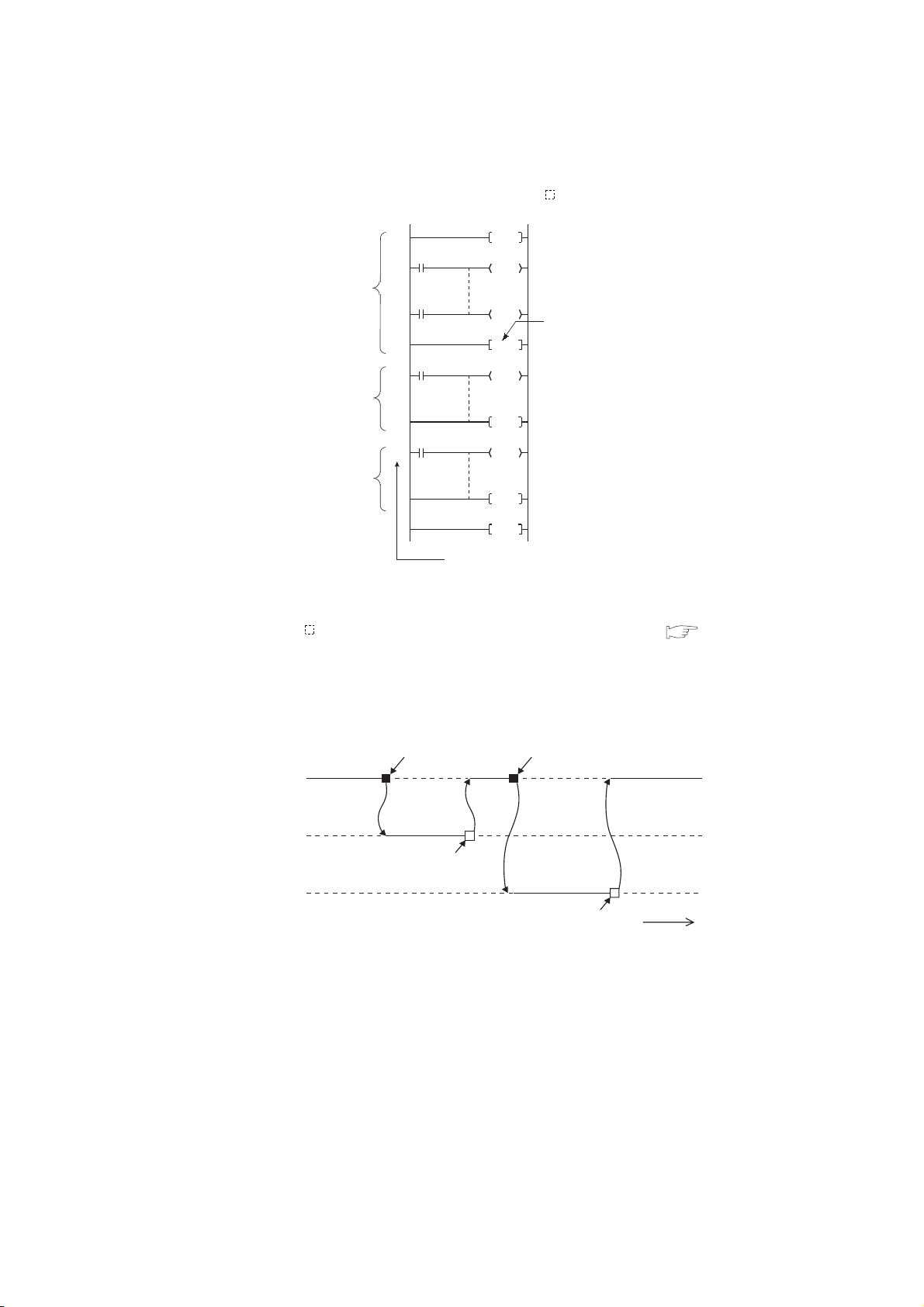
2.2.3 Interrupt program
(1) Definition
Interrupt program is a program from an interrupt pointer (I ) to the IRET instruction.
Main routine
program
EI
FEND
Indicates the end
of the main routine
program.
Interrupt
program (I0)
Interrupt
program (I29)
The interrupt pointer (I ) number varies depending on the interrupt factor. (
I0
IRET
I29
IRET
END
Interrupt pointer
Figure 2.7 Interrupt program
Section 9.11)
When an interrupt factor occurs, the interrupt program of the interrupt pointer number corresponding
to that factor is executed. (Interrupt programs are executed only when the corresponding interrupt
factor occurs.)
Main routine
program
Occurrence of the
interrupt factor for I0
Execution Execution Execution
Occurrence of the
interrupt factor for I29
2 - 6
Interrupt
program (I0)
Interrupt
program (I29)
Execution
IRET
Execution
IRET
Figure 2.8 Interrupt program execution timing
Time
Page 45

CHAPTER2 SEQUENCE PROGRAMS
Only one interrupt program can be created with one interrupt pointer number.
1
EI
FEND
I0
IRET
I29
IRET
END
Interrupt
program (I0)
Interrupt
program (I29)
Remark
For details of the interrupt factors and interrupt pointers, refer to Section 9.11.
(2) Programming of interrupt programs
Create interrupt programs between the FEND and END instructions in the main routine program.
Program A
2
3
4
5
6
7
8
Main routine
program
FEN
I0
Interrupt
program
Figure 2.9 Programming location of interrupt programs
*1: The pointer numbers do not need to be specified in ascending order.
Interrupt programs can be managed as one separate program (stand-by type program). ( Section 2.3.3)
I32
I28
Interrupt pointer
Y10
IRET
Y11
IRET
Y12
IRET
END
*1
2.2 Sequence Program Configuration
2.2.3 Interrupt program
2 - 7
Page 46

(a) Before executing an interrupt program
Before executing the interrupt programs of the interrupt pointers I0 to I15, I28 to I31, I45, and I50 to
I255, enable interrupts with the EI instruction.
Remark
For details of the EI instruction, refer to the following.
QCPU Programming Manual (Common Instructions)
(b) Restrictions on programming
1) PLS and PLF instructions
The PLS and PLF instructions perform off processing in the next scan of which the instruction is
executed.
Therefore, the device which is turned on by the instruction remains on until the same instruction is
reexecuted.
X0
PLS M0
0
OFF
X0
OFF
M0
Figure 2.10 Device turned on by the PLS instruction in the interrupt program
ON
IRET
ENDEND
0
IO
ON
Turns on by executing the PLS M0 instruction at the rise of X0.
END END
0
IO IRET
X0
PLS M0
0
Turns off by executing the
PLS M0 instruction.
2) EI and DI instructions
During execution of an interrupt program, interrupts are disabled (DI) so that any other interrupt
processing will not be executed.
Do not execute the EI or DI instruction during interrupt program execution.
3) Timer (T) and counter (C)
Do not use the timer (T) and counter (C) in interrupt programs.
If more than one interrupts occur in one scan, the timer (T) and counter (C) in the interrupt
program cannot measure the time correctly.
The OUT C instruction status causes the counter (C) measure the number of interrupts
incorrectly.
2 - 8
4) Instructions not available in interrupt programs
Refer to sections corresponding to each instruction in the following.
QCPU Programming Manual (Common Instructions)
Page 47

CHAPTER2 SEQUENCE PROGRAMS
(3) Operation when an interrupt factor occurs
There are restrictions on interrupt programs depending on the interrupt factor occurrence timing.
(a) When an interrupt factor occurs before the interrupt program execution status is enabled
The CPU module stores the interrupt factor occurred.
As soon as the interrupt program execution status is enabled, the CPU module executes the
interrupt program corresponding to the stored interrupt factor.
Interrupt factor
occurrence
Main routine
program
Interrupt
program
Figure 2.11 When an interrupt factor occurs before interrupts are enabled
Not executed because
the interrupt program
execution status is
disabled (DI).
When the same interrupt factor occurs more than one time before the interrupt program execution
status is enabled, the interrupt factors of I0 to I15, I28 to I31, I45, I50 to I255, and fixed scan
execution type programs are stored only once.
Note that all interrupt factors occurred are discarded if they are masked by the IMASK instruction.
Interrupt
enabled (EI)
Execution
Executed as soon as
the interrupt program
execution status
changes to enabled.
1
2
3
4
5
6
7
8
Remark
For details of the IMASK instruction, refer to the following.
QCPU Programming Manual (Common Instructions)
(b) When an interrupt factor occurs in the STOP or PAUSE status
The CPU module executes the interrupt program as soon as the interrupt program execution status is enabled
after the CPU module status is changed to RUN.
STOP/PAUSE
Interrupt factor
occurrence
Main routine
program
Interrupt
program
Figure 2.12 When an interrupt factor occurs in the STOP or PAUSE status
Not executed because
the CPU module is in
the STOP status.
RUN
Interrupt
enabled (EI)
Execution
Executed as soon as the interrupt
program execution status changes
to enabled after the CPU module
status is changed from
STOP/PAUSE to RUN.
2.2 Sequence Program Configuration
2.2.3 Interrupt program
2 - 9
Page 48

(c) When multiple interrupt factors occur simultaneously in the interrupt program execution
enabled status
The interrupt programs are executed in the order of interrupt pointers (I ) with high priority.
(
Section 9.11.1)
Other interrupt programs have to wait until processing of the interrupt program being executed is
completed.
Simultaneous occurrence of
multiple interrupt factors
I50 I100
I150
Execution
IRET
Wait to be
processed
Wait to be processed
Execution
IRET
Execution
IRET
High
Priority
Low
Interrupt
enabled (EI)
Main routine
program
Interrupt
program (I50)
Interrupt
program (I100)
Interrupt
program (I150)
Figure 2.13 When multiple interrupt factors occur simultaneously
(d) When the same interrupt factor as that of the interrupt program being executed occurs
When the same interrupt factor as that of the interrupt program being executed occurs more than
one time before completion of interrupt program processing, the interrupt factors of I0 to I15, I45,
and I50 to I255 are stored only once, and then the interrupt program corresponding to each stored
interrupt factor is executed after completion of current interrupt program execution
.
The interrupt factors of I28 to I31 and fixed scan execution type programs are all stored, and then all
the interrupt programs corresponding to interrupt factors are executed after completion of current
interrupt program execution.
2 - 10
Page 49

CHAPTER2 SEQUENCE PROGRAMS
(e) When an interrupt factor occurs during link refresh
The link refresh is suspended and an interrupt program is executed.
Even if the Block data assurance per station setting is enabled in the CC-Link IE controller network
or MELSECNET/H network, this setting does not work when a device set as a refresh target is used
in the interrupt program.
In the interrupt program, do not use any refresh target device.
10ms 10ms 10ms 10ms
Interrupt factor
Interrupt program
execution
Link refresh execution
Link refresh is suspended and
interrupt program is executed.
Figure 2.14 When an interrupt factor occurs during link refresh
1
2
3
4
5
6
7
Remark
For the Block data assurance per station setting, refer to the following.
Reference manual for each network module
(f) Interrupt during END processing
When the constant scan function is used and an interrupt factor occurs during the waiting time in
END processing, an interrupt program corresponding to the interrupt factor is executed.
(g) When an interrupt factor occurs during access to another module
When an interrupt factor occurs during access to another module (during service processing or instruction
processing), the interrupt program becomes standby status until the service processing or the instruction in
execution is completed.
To shorten the wait time of the interrupt, reduce the amount of data that access to other modules.
8
2.2 Sequence Program Configuration
2.2.3 Interrupt program
2 - 11
Page 50

(4) Processing at program execution type change
When the program execution type is changed from the scan execution type to the interrupt, the CPU
module saves and restores the following data. (
• Data in the index register
• File register block number
Whether to save and restore the data above can be set in the PLC parameter dialog box.
If the data is not saved or restored, the overhead time of the corresponding interrupt program can be shortened.
( Section 10.1.2)
Section 9.6.3)
(5) Restrictions
(a) When the same device is used
During execution of an instruction in a main routine program, an interrupt program may be
executed, suspending the processing of the instruction being executed.
If the same device is used for the main routine program and interrupt program, device data may
become inconsistent. In this case, take the following measures to prevent device data
inconsistency.
1) Moving device data to another device
Do not directly specify the device where the data is written by the interrupt program in the main
routine program. Use the data in another device by moving the data with the transfer instruction.
2) Disabling interrupts with the DI instruction
Disable interrupts with the DI instruction if instructions that may cause inconvenience for the main
routine program are used.
However, interrupts do not occur during access to the device of the corresponding argument of the
instruction. For this reason, data inconsistency will not occur in units of arguments.
2 - 12
Page 51

CHAPTER2 SEQUENCE PROGRAMS
2.3 Settings When Program is Divided
When one sequence program is divided into multiple programs, execution conditions, such as executing a
program only once at start-up or executing a program at fixed intervals, can be set for each program.
(1) Control by multiple programs dividing one program
The CPU module can store multiple programs divided on the basis of each control unit.
This enables programming of one sequence program by two or more designers.
Control by one program
Program A
Control data A
Control data B
Divide one program
into multiple
programs.
Control data A
Program B
Control data B
Program C
The programs divided on
the basis of each control
data are registered.
1
2
3
4
5
6
7
Control data C
Figure 2.15 Control by multiple programs
Control data C
(2) Settings required for execution of multiple programs
To execute multiple programs in the CPU module, names (file names) and execution conditions of the
programs must be set.
Set them in the Program tab of the PLC parameter dialog box.
(a) (b) (b) 4)
Programs are executed
according to the setting
order.
8
2.3 Settings When Program is Divided
(c)
Figure 2.16 Program setting
2 - 13
Page 52

(a) Program name
Enter the name (file name) of the program to be executed in the CPU module.
(b) Execute type
Select an execution type of the program set under "Program name".
The CPU module executes programs whose execution type has been set here according to the
setting order
1) Initial execution type ("Initial")
This program is executed only once when the CPU module is powered on or its status is switched
from STOP to RUN.
2) Scan execution type ("Scan")
This program is executed once in every scan, starting in the next scan of which the initial
execution type program is executed and later.
3) Stand-by type ("Wait")
This program is executed only when its execution is requested.
4) Fixed scan execution type ("Fixed scan")
This program is executed at time intervals specified with fixed scan interval and unit.
( Section 2.3.4)
• Fixed scan interval ("Fixed scan interval")
.
( Section 2.3.1)
( Section 2.3.2)
( Section 2.3.3)
Enter the execution interval of fixed scan execution type program.
The setting range varies depending on the setting unit.
•When the unit is "ms" : 0.5 to 999.5ms (in increments of 0.5ms)
•When the unit is "s" : 1 to 60s (in increments of 1s)
• Unit ("In unit")
Select the unit ("ms" or "s") of the fixed scan interval.
2 - 14
Page 53

CHAPTER2 SEQUENCE PROGRAMS
(c) File usability setting Note2.1Note1
For each program, determine whether to use the file specified for the local device in the PLC file tab
of the PLC parameter dialog box.
Figure 2.17 File usability setting
The default is set to "Use PLC file setting".
When "Not used" is selected, data in the local device is not saved or restored when the program
execution type is changed.
1
2
3
4
5
6
7
8
2.3 Settings When Program is Divided
Note1
Note2.1
Universal
The Q00UJCPU does not support the file usability setting.
When using the file usability setting for the Q02UCPU, Q03UDCPU, Q04UDHCPU, Q06UDHCPU, Q13UDHCPU, or
Q26UDHCPU, check the versions of the CPU module and GX Developer. ( Appendix 2)
2 - 15
Page 54
(3) Program sequence in the CPU module
Figure 2.18 shows the program sequence after the CPU module is powered on or its operating status is changed
from STOP to RUN.
Powered off on/STOP RUN
Initial execution
type program
END processing
Scan execution
type program
Fixed scan
execution type
program
Stand-by
type program
Figure 2.18 Program sequence
Executed only once when
the CPU module is powered
on or its status is switched
from STOP to RUN.
Executed at specified
time intervals.
Executed only when its
execution is requested.
Program execution sequence
Program execution when any
subroutine program or interrupt
program is called
2 - 16
Use initial execution type program, stand-by type program, and fixed scan execution type program as required.
Page 55

CHAPTER2 SEQUENCE PROGRAMS
2.3.1 Initial execution type program
(1) Definition
Initial execution type program is executed only once when the CPU module is powered on or its
operating status is changed from STOP to RUN.
This type of program can be used as a program that need not be executed from the next scan and
later once it is executed, like initial processing to an intelligent function module.
Control by one program
Processing performed
only once
Processing performed
in every scan
Figure 2.19 When processing performed only once is separated as an initial execution type program
(2) Processing
When an initial execution type program is used
Program A
Initial execution type
program
One program can
be divided into two
Program B
Scan execution type
program
programs.
1
2
3
4
5
6
7
(a) Execution order
After completion of all the initial execution type program execution, END processing is performed.
In the next scan and later, scan execution type programs are executed.
Powered off on/
STOP RUN
Initial execution
type program A
Initial execution
type program B
Initial execution
type program n
END processing
Scan execution type
program
Figure 2.20 Execution order of the initial execution type programs
1 scan
If there are multiple initial
execution type programs, the
CPU module executes them in
ascending order of the setting.
2.3.1 Initial execution type program
8
2.3 Settings When Program is Divided
2 - 17
Page 56

(b) Initial scan time
Initial scan time is the execution time of initial execution type program.
When multiple programs are executed, the initial scan time will be the time required for completing
all the initial execution type program execution.
1) Initial scan time storage location
The CPU module measures the initial scan time and stores it into the special register (SD522 and
SD523).
The initial scan time can be checked by monitoring SD522 and SD523.
SD522 SD523
Stores the initial scan time of 1ms or less (unit: s).
Stores the initial scan time. (unit: ms).
Figure 2.21 Initial scan time storage location
Example
time is 3.4ms.
If the stored values in SD522 and SD523 are 3 and 400 respectively, the initial scan
2) Accuracy and measurement of the initial scan time
Accuracy of the initial scan time stored in the special register is 0.1ms.
Even if the WDT instruction (instruction that resets the watchdog timer) is executed in the
sequence program, the measurement of the initial scan time continues.
3) Execution of an interrupt program or fixed scan execution type program
When an interrupt program or fixed scan execution type program is executed before completion of
the initial execution type program execution, the execution time of the executed program will be
added to the initial scan time.
(3) Precautions on programming
Initial execution type programs do not support the instructions that require several scans (instructions
with completion device).
Example
SEND, RECV, and similar instructions
2 - 18
Page 57

CHAPTER2 SEQUENCE PROGRAMS
(4) Initial execution monitoring time setting
Initial execution monitoring time is a timer for monitoring initial scan time.
Set a time value in the PLC RAS tab of the PLC parameter dialog box.
The setting range is 10 to 2000ms (in increments of 10ms).
No default value is set.
Figure 2.22 PLC RAS setting (Initial execution monitoring time)
(a) When the initial scan time exceeds the preset initial execution monitoring time
"WDT ERROR" occurs and the CPU module stops program operations.
Set a time value so that the initial execution monitoring time becomes longer than actual initial scan
time.
1
2
3
4
5
6
7
An error of the measurement value is 10ms for the initial execution monitoring time setting.
If the initial execution monitoring time (t) parameter is set to 10ms, "WDT ERROR" occurs when actual initial
scan time is within the range of 10ms < t < 20ms.
2.3.1 Initial execution type program
8
2.3 Settings When Program is Divided
2 - 19
Page 58
2.3.2 Scan execution type program
(1) Definition
Scan execution type program is executed once in every scan, starting in the next scan of which the
initial execution type program is executed and later.
STOP RUN
Power supply ON RUN
1st scan 2nd scan 3rd scan 4th scan
END processing
Initial execution type program
Scan execution type program A
0 END
0 END
Scan execution type program B
0 END
Scan execution type program C
Scan time
Figure 2.23 Execution order of the scan execution type programs
0 END
0 END
0 END
0 END
(2) Processing
When multiple scan execution type programs are executed, the scan time will be the time required for
completing all the scan execution type program execution.
If an interrupt program or fixed scan execution type program is executed, execution time of the
executed program will be added to the scan time.
0
2 - 20
Page 59

CHAPTER2 SEQUENCE PROGRAMS
2.3.3 Stand-by type program
(1) Definition
Stand-by type program is executed only when its execution is requested.
This type of program can be changed to any desired execution type by a sequence program
instruction.
(2) Application
(a) Program library
Stand-by type program is used as a program library, a collection of subroutine programs and/or
interrupt programs, and managed separately from a main routine program.
Multiple subroutine programs and/or interrupt programs can be created and managed in a single
stand-by type program.
Scan execution type program Scan execution type program
Main routine
program
P100
Subroutine
program
Main routine
program
Stand-by type program
1
2
3
4
5
6
7
Interrupt
I0
program
Figure 2.24 Program library using a stand-by type program
P100
I0
Subroutine
program
Interrupt
program
(b) Program type change
Stand-by type program is used to create and store programs available in all systems. Only required
programs will be executed.
For example, a program preset as a stand-by ("Wait") type program in the PLC parameter dialog
box can be changed to a scan execution type program and executed in the sequence program.
8
2.3 Settings When Program is Divided
2.3.3 Stand-by type program
2 - 21
Page 60

(3) Execution method
Execute stand-by type programs in either of the following methods.
• Create subroutine and/or interrupt programs in a stand-by type program and call them using a
pointer or when an interrupt occurs.
• Change a stand-by type program to any other execution type using instructions.
(a) Creating subroutine and/or interrupt programs in a single stand-by type program
When creating subroutine and/or interrupt programs in a single stand-by type program, start the
program from the step 0.
The FEND instruction used in creation of a subroutine or interrupt program is not required after a
main routine program.
Program A
Main routine
program
Program B (Stand-by type program)
P500
P508
P501
Use common pointer.
Figure 2.25 Creating subroutine programs in a single stand-by type program
Y10
RET
Y11
RET
Y12
RET
END
2 - 22
Page 61

CHAPTER2 SEQUENCE PROGRAMS
1) Executing a subroutine program and interrupt program in a stand-by type program
After execution of the stand-by type program, the CPU module reexecutes the program that called a program
in the stand-by type program.
Figure 2.26 shows the operation when the subroutine and interrupt programs in the stand-by type program
are executed.
CALL P100
instruction execution
END processing END processing END processing
Main routine program
Subroutine program within
a stand-by type program
Interrupt program within a
stand-by type program
Figure 2.26 Operation when the subroutine and interrupt programs in the stand-by type program are executed
● For restrictions on programming of subroutine and interrupt programs, refer to the following.
• Subroutine program: Section 2.2.2
• Interrupt program: Section 2.3.2
P100 RET
Interrupt factor
occurrence
I0 IRET
1
2
3
4
5
6
7
8
● Use common pointers. ( Section 9.10.2)
If local pointers are used, subroutine programs in a stand-by type program cannot be executed from any other program.
2.3 Settings When Program is Divided
2.3.3 Stand-by type program
2 - 23
Page 62
(b) Changing the program execution type using instructions
Use the PSCAN, PSTOP, or POFF instruction to change a program execution type.
1) Changing the execution type (in the case of scan execution type program)
• Set the programs "ABC" and "GHI" as scan execution type programs and the program "DEF" as a standby type program.
• When the condition is established (the internal relay (M0) in Figure 2.27 turns on), the program "DEF" is
changed to a scan execution type program and the program "ABC" to a stand-by type program.
[Before execution of the PSCAN and PSTOP instructions]
Scan execution type program: ABC
MO
PSCAN "DEF"
PSTOP "ABC"
• The PSCAN instruction changes the program "DEF" to
a scan execution type program.
• The PSTOP instruction changes the program "ABC" to
a stand-by type program.
Stand-by type program: DEF Scan execution type program: GHI
PSCAN "GHI"
PSTOP "DEF"
When M0 turns on
[After execution of the PSCAN and PSTOP instructions]
Stand-by type program: ABC
PSCAN "ABC"
PSTOP "GHI"
2 - 24
PSCANMO"DEF"
PSTOP "ABC"
Scan execution type program: DEF Scan execution type program: GHI
PSCAN "GHI"
PSTOP "DEF"
Figure 2.27 Example of changing the execution type (in the case of scan execution type program)
PSCAN "ABC"
PSTOP "GHI"
Page 63

CHAPTER2 SEQUENCE PROGRAMS
2) Execution type change timing
The program execution type is changed in END processing.
Therefore, the execution type will not be changed in the middle of program execution.
If different types are set to the same program in the same scan, the program will be changed to the type
specified by the last instruction executed.
END processing END processing END processing
Program name
*1: The programs "GHI" and "DEF" are executed in the order set in the Program tab of the PLC parameter dialog box.
"GHI" "GHI" "GHI"
"ABC"
PSTOP "ABC"
execution
PSCAN "DEF"
execution
Figure 2.28 Execution type change timing
*1
"GHI"
"DEF" is changed to a scan execution type
program and "ABC" is changed to a stand-by
type program.
"DEF"
*1
(4) Precautions on programming
(a) Unavailable devices
Unavailable devices depend on the program type (subroutine program or interrupt program) or the execution
type changed by an instruction.
1
2
3
4
5
6
7
(b) Use of local devices
For execution of a subroutine program using a local device, refer to Section 9.14.2.
8
2.3 Settings When Program is Divided
2.3.3 Stand-by type program
2 - 25
Page 64

2.3.4 Fixed scan execution type program
(1) Definition
Fixed scan execution type program is a program executed at specified time intervals.
This type of programs, unlike interrupt programs, can be interrupted in units of files without interrupt
pointers or the IRET instruction.
For the restrictions on programming, refer to
(The restrictions on programming are the same as those for interrupt programs.)
Fixed scan interval
Section 2.2.3(2)(b).
END processing
Scan execution
type program
Fixed scan execution
type program
Figure 2.29 Execution of a fixed scan execution type program
To execute a fixed scan execution type program, execute the EI instruction in the initial execution type program
or scan execution type program to enable interrupts.
Condition
established
Condition
established
2 - 26
Page 65

CHAPTER2 SEQUENCE PROGRAMS
(2) Processing
(a) When two or more fixed scan execution type programs exist
Each fixed scan execution type program is executed at specified time intervals.
If two or more fixed scan execution type programs reach the specified time at the same timing,
programs will be executed in ascending order of the numbers set in the Program tab of the PLC
parameter dialog box.
(b) When both fixed scan execution type program and interrupt program exist
When a fixed scan execution type program and an interrupt program (I28 to I31) reach the specified
time at the same timing, the interrupt program will be given priority.
(c) When the execution condition is established during link refresh
The link refresh is suspended and a fixed scan execution type program is executed.
Even if the Block data assurance per station setting is enabled in the CC-Link IE controller network or
MELSECNET/H network, this setting does not work when a device set as a refresh target is used in the fixed
scan execution type program.
In the fixed scan execution type program, do not use any refresh target device.
10ms 10ms 10ms 10ms
1
2
3
4
5
6
7
8
Interrupt factor
Fixed scan execution type
program execution
Link refresh execution
Figure 2.30 When the execution condition is established during link refresh
Remark
For the Block data assurance per station setting, refer to the following.
Reference manual for each network module
Link refresh is suspended and fixed scan
execution type program is executed.
2.3 Settings When Program is Divided
2.3.4 Fixed scan execution type program
2 - 27
Page 66

(d) When the execution condition is established during END processing
When the execution condition is established during the waiting time of the constant scan execution
or the END instruction, a fixed scan execution type program is executed.
Constant scan
*2
Fixed scan interval
END processing
Scan execution
type program
Fixed scan execution
type program
Figure 2.31 When the execution condition is established during the waiting time
Condition
established
*1: Waiting time
*2: If processing is not completed within the
waiting time, the scan time increases.
*1
(3) Processing at program execution type change
For how to save and restore data in the index register when the program execution type is changed, refer to
Section 2.2.3(4). (The method is the same as that for interrupt programs.)
2 - 28
Page 67

CHAPTER2 SEQUENCE PROGRAMS
(4) Precautions
(a) Execution interval of a fixed scan execution type program
Execution interval of a fixed scan execution type program may increase from the preset interval
depending on the time set for disabling interrupts by the DI instruction (interrupt disabled time).
If the interrupt disabled time by the DI instruction becomes too long, use an interrupt program by
fixed scan interrupt (I28 to I31) instead of a fixed scan execution type program.
Highest common factor of fixed scan execution interval
*1: This is the highest common factor of execution interval set to multiple fixed scan execution type programs
When the condition 1) is satisfied, the actual execution interval of a fixed scan execution type
program may increase from the preset interval by the time shown in the expression below.
Interrupt disabled time
Highst common factor of scan
execution interval
Fixed scan execution interval set to
the corresponding program
The following shows an example of the increase in execution time of a fixed scan execution type
program.
*1
< Interrupt disabled time ••• Condition 1)
1
2
3
4
5
6
7
8
Example
• Fixed scan execution interval ••• 10ms, 5ms, 1ms, 0.5ms
• Highest common factor of fixed scan execution interval ••• 0.5ms
• Interrupt disabled time (DI) ••• 5ms
(Interrupt enabled time (EI) ••• less than 0.5ms)
With the settings above, the condition 1) will be 0.5ms < 5ms.
Program execution
operation
Interrupt enabled/
disabled status
n scan
DI
Disabled Disabled Disabled
Interrupt disabled time = 5ms Interrupt disabled time = 5ms
Figure 2.32 Program execution and interrupt enabled/disabled status
EI
END END
Enabled
Less than 0.5ms Less than 0.5ms
DI
n+1 scan
EI
Enabled
2.3 Settings When Program is Divided
2.3.4 Fixed scan execution type program
The execution time of a fixed scan execution type program whose execution interval is set to 10ms
increases 100ms (5 0.5 10 = 100) at the most.
2 - 29
Page 68

2.3.5 Changing the program execution type
(1) Changing the execution type using instructions
(a) Instructions used to change the execution type
The execution type of sequence programs can be changed using instructions even during
execution.
Use the PSCAN, PSTOP, or POFF instruction to change the execution type.
PSCAN
Initial execution
type program
instruction
Scan execution
type program
PSTOP, POFF
instruction
Stand-by type
program
Figure 2.33 Pattern of execution type change
Table2.1 Timing of execution type change
Execution type before
change
PSCAN PSTOP POFF
Scan execution type Remains unchanged.
Initial execution type
Stand-by type
Fixed scan execution
type
Changes to the scan
execution type.
Changes to the scan
execution type.
Changes to the scan
execution type.
PSTOP, POFF
instruction
PSCAN
instruction
Fixed scan execution
type program
PSTOP, POFF
instruction
Changes to the stand-by
type.
Changes to the stand-by
type.
PSCAN
instruction
Instruction
Turns off outputs in the next scan.
Changes to the stand-by type in two
scans later.
Turns off outputs in the next scan.
Changes to the stand-by type in two
scans later.
Remains unchanged. No processing
Changes to the stand-by
type.
Turns off outputs in the next scan.
Changes to the stand-by type in two
scans later.
2 - 30
Once the fixed scan execution type program is changed to another execution type, the type cannot be returned
to the fixed scan execution type.
Page 69

CHAPTER2 SEQUENCE PROGRAMS
(b) Execution type change example
In a control program, a stand-by type program matching the preset condition is changed to a scan
execution type program in the course of program execution.
An unused scan execution type program can also be changed to a stand-by type program.
Figure 2.34 shows the case where the execution type of the stand-by type programs "ABC", "DEF",
"GHI", and "JKL" are changed in the control program.
When M0 turns on, the
program "ABC" is
changed from a stand-by
type to a scan execution
type program.
When M1 turns on, the
program "ABC" is
changed from a scan
execution type to a
stand-by type program.
Control program
M0
M1
PSCAN
PSTOP
PSCAN
PSTOP
"ABC"
"ABC"
"DEF"
"DEF"
The PSCAN instruction
changes the program "ABC" to
a scan execution type program.
The PSTOP instruction changes
the program "ABC" to a standby type program.
1
2
3
4
5
6
7
Stand-by
type
program
:ABC
Figure 2.34 Execution type change example
Stand-by
type
program
:DEF
Stand-by
type
program
:GHI
Stand-by
type
program
:JKL
(2) Changing the execution type from the Program monitor list screen
The execution type of programs can be changed on the screen opened by selecting [Online]
[Monitor] [Program monitor list].
( Section 6.13.1)
2.3.5 Changing the program execution type
8
2.3 Settings When Program is Divided
2 - 31
Page 70

2.4 Data Used in Sequence Programs
The CPU module represents numeric and alphabetic data using two symbols (states): 0 (off) and 1 (on).
Data represented using these two symbols is called binary number (BIN).
The CPU module can also use hexadecimal (HEX) (each hexadecimal digit represents four binary bits), binary-coded
decimal (BCD), or real numbers.
Ta bl e 2 .2
DEC (Decimal) HEX (Hexadecimal) BIN (Binary) BCD (Binary-coded decimal)
shows the numeric representations of BIN, HEX, BCD, and DEC (decimal).
Table2.2 Numeric representations of BIN, HEX,BCD,and DEC
00 0 0
11 1 1
22 10 10
3 3 11 11
9 9 1001 1001
10 A 1010 1 0000
11 B 1011 1 0001
12 C 1100 1 0010
13 D 1101 1 0011
14 E 1110 1 0100
15 F 1111 1 0 101
16 10 1 0000 1 0110
17 11 1 0001 1 0111
47 2F 1 0 1111 10 0 0111
32766 7FFE 0111 1111 1111 1110 -
32767 7FFF 0111 1111 1111 1111 -
-32768 8000 1000 0000 0000 0000 1000 0000 0000 0000
-32767 8001 1000 0000 0000 0001 1000 0000 0000 0001
-2 FF FE 1111 1111 1111 111 0 -
-1 FFF F 1111 1111 1111 1111 -
2 - 32
Page 71

CHAPTER2 SEQUENCE PROGRAMS
(1) Inputting numeric values externally to the CPU module
When setting a numeric value to the CPU module externally using a digital switch, BCD (binary-coded decimal)
can be used as DEC (decimal) by the method given in (b).
(a) Numeric values used inside the CPU module
The CPU module performs program operations in binary.
If the value set in binary-coded decimal is used without conversion, the CPU module performs program
operations regarding the set value as binary.
Therefore, the program operations are not performed correctly. ( (b) below)
(b) Using any numeric data regardless of the data type
To convert the data set in binary-coded decimal into binary, which can be used in the CPU module, use the BIN
instruction.
The BIN instruction allows the CPU module to use any external numeric data regardless of the data type.
CPU module
[Setting numeric data]
Digital switch
4321
XF X0to
Input data in BCD.
BINP K4X0 DO
BIN data
BCD D5 K4Y30
1
2
3
4
5
6
7
Figure 2.35 Inputting data from a digital switch to the CPU module
Remark
For details of the BIN instruction, refer to the following.
QCPU Programming Manual (Common Instructions)
8
2.4 Data Used in Sequence Programs
2 - 33
Page 72

(2) Outputting numeric values externally from the CPU module
When externally displaying numeric values operated in the CPU module, a digital indicator can be used.
(a) Outputting numeric values
The CPU module performs program operations in binary.
If the binary values used in the CPU module are output to a digital indicator, the indicator does not show the
values correctly.
To convert the data set in binary into binary-coded decimal, which can be used in the external indicator, use the
BCD instruction.
The BCD instruction allows the external indicator to display values in decimal.
CPU module
[Setting numeric data]
BINP K4X0 DO
Digital indicator
Y3F Y30to
BCD D5 K4Y30
Figure 2.36 Display of operation results in the CPU module by a digital indicator
Remark
For details of the BCD instruction, refer to the following.
QCPU Programming Manual (Common Instructions)
Output data
in BCD.
BIN data
2 - 34
Page 73

CHAPTER2 SEQUENCE PROGRAMS
2.4.1 BIN (Binary Code)
(1) Definition
Binary is a numeral system that represents numeric values using two symbols, 0 (off) and 1 (on).
Decimal notation uses the symbols 0 through 9. When the symbols for the first digit are exhausted (a
digit reaches 9), the next-higher digit (to the left) is incremented, and counting starts over at 0.
In binary notation, only the symbols 0 and 1 are used. After a digit reaches 1, an increment resets it to
0 and the next digit (to the left) is incremented. (The numeric value becomes 10, which is equal to 2 in
decimal.)
Table2.3 shows the numeric representations in BIN and DEC.
Table2.3 Numeric representations in BIN and DEC
DEC (Decimal) BIN (Binary)
0 0000
1 0001
2 0010
3 0011
4 0100
5 0101
60110
7 0111
8 1000
9 1001
10 1010
11 1011
Carry
Carry
Carry
1
2
3
4
5
6
7
8
2.4 Data Used in Sequence Programs
2.4.1 BIN (Binary Code)
2 - 35
Page 74

(2) Numeric representation in BIN
(a) Bit configuration of BIN used in the CPU module
Each register (such as the data register, link register) in the CPU module consists of 16 bits.
(b) Numeric data available in the CPU module
Each register in the CPU module can store numeric values in the range of -32768 to 32767.
Figure 2.37 shows the numeric representations for registers.
Most significant bit (sign bit)
b15
Bit name
b14 b13 b12 b11 b10 b9 b8 b7 b6 b5 b4 b3 b2 b1 b0
0
Decimal value
Figure 2.37 Numeric representations for registers in the CPU module
2152142132122112102928272625242322212
8192
-32768
16384
4096 2048 1024 512 256 128 64 32 16 8 4 2 1
A value will be negative value when the most significant bit is "1".
A numeric value of 2n is assigned for each bit of registers.
Note that an unsigned binary number (0 to 65535) cannot be used in the most significant bit position since the
most significant bit is a sign bit.
• The most significant bit is "0"...Positive
• The most significant bit is "1"...Negative
2 - 36
Page 75

CHAPTER2 SEQUENCE PROGRAMS
2.4.2 HEX (Hexadecimal)
(1) Definition
Hexadecimal (HEX) is a numeral system that represents four binary bits as one digit.
With four binary bits, sixteen different numeric values, 0 to 15, can be represented.
Hexadecimal notation uses 16 symbols to represent numeric values 0 to 15 in one digit, the symbols 0
to 9 to represent values zero to nine, and A
reaches F
ï\2.4 shows the numeric representations in BIN, HEX, and DEC.
H, the next-higher digit (to the left) is incremented.
Table2.4 Numeric representations in BIN,HEX,and DEC
DEC (Decimal) HEX (Hexadecimal) BIN (Binary)
0 0 0
1 1 1
22 10
33 11
9 9 1001
10 A 1010
11 B 1011
12 C 1100
13 D 1101
14 E 111 0
15 F 1111
16 10 1 0000
17 11 1 0001
47 2 F 10 1111
H to FH to represent values ten to fifteen. After a digit
Carry
2.4.2 HEX (Hexadecimal)
1
2
3
4
5
6
7
8
2.4 Data Used in Sequence Programs
(2) Numeric representation in HEX
Each register (such as the data register, link register) in the CPU module consists of 16 bits.
In the 16-bit configuration register, 0 to FFFF
H can be specified in hexadecimal.
2 - 37
Page 76

2.4.3 BCD (Binary-coded Decimal)
(1) Definition
BCD is a numeral system that uses four binary bits to represent the decimal digits 0 through 9.
The difference from hexadecimal is that BCD does not use letters A to F.
Table2.5
shows the numeric representations in BIN, BCD, and DEC.
Table2.5 Numeric representations in BIN,BCD,and DEC
DEC (Decimal) BIN (Binary) BCD (Binary-coded Decimal)
0 0000 0
1 0001 1
20010 10
3 0011 11
4 0100 100
5 0101 101
6 0110 110
7 0 111 111
8 1000 1000
9 1001 1001
10 1010 1 0000
11 1011 1 0001
12 1100 1 0010
Carry
(2) Numeric representation in BCD
Each register (such as the data register, link register) in the CPU module consists of 16 bits.
Therefore, the numeric values can be stored in each register are those in the range between 0 to 9999 in BCD.
2 - 38
Page 77

CHAPTER2 SEQUENCE PROGRAMS
2.4.4 Real number (Floating-point data)
There are two types of real number data: single-precision floating-point data and double-precision
floating-point data.
(1) Single-precision floating-point data
(a) Internal representation
Internal representation of real numbers used in the CPU module is given below.
Real number data can be represented as follows, using two word devices.
[Sign] 1. [Mantissa] 2
The bit configuration and the meaning of each bit are described below.
b31 b30
b31
Sign
to
b30 to b23
Exponent (8 bits)
[Exponent]
b23 b22
Figure 2.38 Bit configuration of real number data
to
b16 b15
b22 to b0
Mantissa (23 bits)
to
1
2
3
4
5
6
b0
7
1) Sign
The most significant bit, b31, is the sign bit.
0: Positive
1: Negative
2) Exponent
The 8 bits, b23 to b30, represent the excess n of 2n.
The following shows the excess n according to the binary values in b23 to b30.
b23 to b30
n
Not used
FEH
H
FF
127
Figure 2.39 Relation between the exponent and excess n
FD
126
H
81
H
H
80
2
H
7F
1
0
7E
-1
H
02H
-125
01
-126
H
Not used
00
H
3) Mantissa
Each of the 23 bits, b0 to b22, represents the "XXXXXX..." portion when the data is represented in binary,
"1.XXXXXX...".
8
2.4 Data Used in Sequence Programs
2.4.4 Real number (Floating-point data)
2 - 39
Page 78

(b) Calculation example
Calculation examples are shown below. (The "X" in (nnnnnn) x indicates the numeral system used.)
1) Storing "10"
(10)10 (1010)
2
(1.010000..... 23)
2
Sign: Positive 0
Exponent: 3 82H (10000010)
Mantissa: (010 00000 00000 00000 00000)
2
2
In this case, the value will be encoded as 41200000H.
Sign Exponent Mantissa
0 1 0 0 0 0 0 1 0 0 1 0 0 0 0 0 0 0 0 0 0 0 0 0 0 0 0 0 0 0 0 0
41 2 00000
2) Storing "0.75"
(0.75)10 (0.11)
2
(1.100..... 2-1)
Sign: Positive 0
Exponent: -1 7E
H (01111110)2
Mantissa: (100 00000 00000 00000 00000)2
2
In this case, the value will be encoded as 3F400000H.
Sign Exponent Mantissa
0 0 1 1 1 1 1 1 0 1 0 0 0 0 0 0 0 0 0 0 0 0 0 0 0 0 0 0 0 0 0 0
3F4 00000
Values after the decimal point (in binary) is calculated as follows.
Example
(0.1101)
2 = 2
(0.1101)
-1
2
0.1101
-1
The bit represents 2-2The bit represents 2-3The bit represents 2
+ 2-2 + 2
The bit represents 2
-4
= 0.5 + 0.25 + 0.0625 = (0.8125)10
-4
2 - 40
Page 79

CHAPTER2 SEQUENCE PROGRAMS
(2) Double-precision floating-point data
(a) Internal representation
Real number data used in the CPU module is internally represented as follows, using four word
devices.
[Sign] 1. [Mantissa] 2
The bit configuration and the meaning of each bit are described below.
b63 b62
b63
Sign
to
b52 to b62
Exponent (11 bits)
1) Sign
The most significant bit, b63, is the sign bit.
0: Positive
1: Negative
[Exponent]
b52 b51
Figure 2.40 Bit configuration of real number data
to
b16 b15
b0 to b51
Mantissa (52 bits)
to
1
2
3
4
b0
5
6
7
2) Exponent
The 11 bits, b52 to b62, represent the excess n of 2n.
The following shows the excess n according to the binary values in b52 to b62.
b52 to b62
n
7FF
7FEH
H
1023
H
7FD
1022
Figure 2.41 Relation between the exponent and excess n
400
H
H
3FF
2
H
3FE
3FD
1
0
-1
H
H
3FC
-2
02H
-1021
01
-1022
H
H
00
Not usedNot used
3) Mantissa
Each of the 52 bits, b0 to b51, represents the "XXXXXX..." portion when the data is represented in binary,
"1.XXXXXX...".
8
2.4 Data Used in Sequence Programs
2.4.4 Real number (Floating-point data)
2 - 41
Page 80

(b) Calculation example
Calculation examples are shown below. (The "X" in (nnnnnn) x indicates the numeral system used.)
1) Storing "10"
(10)10 (1010)2 (1.010000..... 23)
2
Sign: Positive 0
Exponent: 3 401H (100 0000 0001)
Mantissa: (0100 0000 0000 0000 0000 0000 0000 0000 0000 0000 0000 0000 0000)
2
2
In this case, the value will be encoded as 4014000000000000H.
Sign Exponent Mantissa
0 100000000010100000000000000000000000000000000000000000000000000
4 014000000000000
2) Storing "0.75"
(0.75)10 (0.11)2 (1.100..... 2-1)
Sign: Positive 0
Exponent: -1 3FDH (011 1111 1101 ) 2
Mantissa: (1000 0000 0000 0000 0000 0000 0000 0000 0000 0000 0000 0000 0000)2
In this case, the value will be encoded as 3FD8000000000000H.
2
Sign Exponent Mantissa
0 011111111011000000000000000000000000000000000000000000000000000
3 FD8000000000000
Values after the decimal point (in binary) is calculated as follows.
Example
(0.1101)
2 = 2
(0.1101)
-1
2
0.1101
-1
The bit represents 2-2The bit represents 2-3The bit represents 2
+ 2-2 + 2
The bit represents 2
-4
= 0.5 + 0.25 + 0.0625 = (0.8125)10
-4
2 - 42
Page 81

CHAPTER2 SEQUENCE PROGRAMS
2.4.5 Character string data
(1) Definition
The CPU module uses ASCII code data.
(2) ASCII code character strings
Ta bl e2 .6 lists the ASCII code character strings.
"00
H" (NULL code) in Table2.6 is used at the end of a character string as a terminator.
0000000011111111
0000111100001111
0011001100110011
0101010101010101
b8 b7 b6 b5 b4 b3 b2 b1 Low
00000
0011
0
0102
0
0123456789ABCDEF
NULL (SP)
Table2.6 ASCII code character strings
Column
P
@
0
Q
A
1
!
R
B
2
"
p
`
q
a
r
b
1
2
3
4
5
6
7
0113
0
1004
0
1015
0
1106
0
11
0
0008
1
0019
1
010A
1
011B
1
1
10
1
10
1
11
1
11
17
C
0
D
1
E
0
F
1
#
$
%
&
'
(
)
+
(Comma)
,
(Minus)
-
(Period)
z
/
S
C
3
s
c
8
T
D
4
U
E
5
V
F
6
W
G
7
X
H
8
Y
I
9
Z
J
:
[
K
;
\
L
<
]
M
=
^
N
>
(Under
line)
O
?
_
t
d
u
e
2.4 Data Used in Sequence Programs
v
f
w
g
x
h
y
i
z
j
{
k
|
l
}
m
n
o
2.4.5 Character string data
2 - 43
Page 82

CHAPTER3 CPU MODULE OPERATION
This chapter describes operation of the CPU module.
3.1 Initial Processing
The CPU module performs preprocessing required for sequence program operations.
The preprocessing is executed only once when any of the operations described in
the CPU module.
When initial processing is completed, the CPU module will be placed in the operation status set by the
RUN/STOP/RESET switch. (
Section 3.5)
Table3.1 Initial processing list
Ta bl e 3 .1 is performed to
Initial processing item
Powered-on Reset
The I/O module initialization
Boot from a memory card
PLC parameter check
Multiple CPU system parameter consistency check
Initialization of devices outside the latch range
(bit device: off, word device: 0)
Automatic I/O number assignment of mounted modules
CC-Link IE controller network and MELSECNET/H
information setting
Intelligent function module switch setting
CC-Link information setting
Ethernet information setting
Initial device value setting
Serial communication function setting
*1: The operation indicates that the status is changed back to RUN without resetting the module after any parameter or program was changed
in the STOP status.
(The RUN/STOP/RESET switch is set from STOP to RUN (the RUN LED will flash), then back to STOP and to RUN again.)
Note that the PLS P instruction (instruction for pulse conversion) may not be executed properly with the above operation. This is
because the previous information may not be inherited depending on the program changes.
CPU module status
Changed from STOP to RUN
: Performed, : Not performed
*1
3 - 1
If any parameter or program is changed in the STOP status, reset the CPU module using the RUN/STOP/RESET switch.
RUN/STOP/RESET switch
RUN
RESET
STOP
Page 83

CHAPTER3 CPU MODULE OPERATION
3.2 I/O Refresh (Refresh Processing with Input/Output Modules)
The CPU module performs the following before sequence program operations.
• On/off data input from the input module or intelligent function module to the CPU module
• On/off data output from the CPU module to the output module or intelligent function module
When the constant scan time is set, I/O refresh is performed after the constant scan waiting time has
elapsed.
(I/O refresh is performed at each constant scan cycle.)
3.3 Program Operation
The CPU module sequentially executes the program stored in the module from the step 0 to the END or
FEND instruction.( CHAPTER 2)
3.4 END Processing
1
2
3
4
5
6
7
The CPU module performs refresh processing with network modules and communication with external
devices.
END processing includes the following.
• Refresh with network modules ( CHAPTER 10)
• Auto refresh with intelligent function module ( Section 7.1.1)
• Intelligent function module dedicated instruction processing ( CHAPTER 10)
• Device data latch processing ( Section 6.3, CHAPTER 10)
• Service processing ( Section 6.24, CHAPTER 10)
• Watchdog timer reset ( Section 6.16)
• Auto refresh between multiple CPU modules ( QCPU User's Manual (Multiple CPU System))
• Device data collection using the sampling trace function (only when trace point is set to every scan (after
END instruction execution)) ( Section 6.14)
• Self-diagnostics processing ( Section 6.17)
• Special relay/special register value setting (only for those that should be set during END processing)
( CHAPTER 12)
8
3.2 I/O Refresh (Refresh Processing with Input/Output Modules)
When the constant scan function ( Section 6.2) is used, the results of processing performed in
END processing are held for the period between after END processing is completed and until the
next scan starts.
3 - 2
Page 84

3.5 Operation Processing in the RUN,STOP, or PAUSE Status
There are three types of operating status of the CPU module.
•RUN status
•STOP status
•PAUSE status
This section describes program operation processing in the CPU module based on its operating status.
(1) Operation processing in the RUN status
RUN status is a status where sequence program operations are repeatedly performed in a loop
between the step 0 and the END (FEND) instruction.
(a) Output status when entering the RUN status
The CPU module outputs either of the following according to the output mode parameter setting when its status
is changed to RUN. ( Section 6.4)
• Output (Y) status saved immediately before entering the STOP status
• Result of operations performed for one scan after entering the RUN status
(b) Processing time required before operations
The processing time required for the CPU module to start sequence program operations after its
operating status is changed from STOP to RUN varies depending on the system configuration and/
or parameter settings. (It takes one to three seconds normally.)
(2) Operation processing in the STOP status
STOP status is a status where sequence program operations are stopped by the RUN/STOP/RESET
switch or the remote STOP function (
The CPU module status will be changed to STOP when a stop error occurs.
Section 6.6.1).
(a) Output status when entering the STOP status
When entering the STOP status, the CPU module saves data in the output (Y) and turns off all
outputs.
The device memory other than that of the output (Y) will be held.
(3) Operation processing in the PAUSE status
PAUSE status is a status where sequence program operations are stopped by the remote PAUSE
function (
device memory status.
Section 6.6.2) after operations are performed for one scan, holding the output and
3 - 3
Page 85

CHAPTER3 CPU MODULE OPERATION
(4) Operation processing in the CPU module when switch operation is performed
Table3.2 Operation processing when switch operation is performed
CPU module operation processing
RUN/STOP
status
RUN
STOP
STOP
RUN
Sequence program
operation
processing
The CPU module
executes the program
until the END
instruction and stops.
The CPU module
executes the program
from the step 0.
External output
The CPU module saves
the output (Y) status
immediately before its
status is changed to
STOP and turns off all the
outputs.
The CPU module outputs
data according to the
output mode parameter
setting.
( Section 6.4)
Device memory
M,L,S,T,C,D Y
The CPU module holds the device
memory status immediately before its
status is changed to STOP.
The CPU module holds the device
memory status immediately before its
status is changed to STOP.
Note that the CPU module uses initial
device values if those values are
preset.
Local device data are cleared.
The CPU module saves
the output (Y) status
immediately before its
status is changed to
STOP and turns off all the
outputs.
The CPU module outputs
data according to the
output mode parameter
setting.
( Section 6.4)
1
2
3
4
5
6
7
The CPU module performs the following in any of the RUN, STOP, or PAUSE status.
• Refresh processing with I/O modules
• Refresh processing with network modules
• Auto refresh processing with intelligent function modules
• Self-diagnostics processing
• Service processing
• Intelligent function module dedicated instruction processing (completion processing only)
• Operation processing of Multiple CPU high speed transmission function
Even if the CPU module is in the STOP or PAUSE status, the following operations can be executed.
• I/O monitor or test operation from GX Developer
• Read/write data from/to external devices using the MC protocol
• Communication with other stations using CC-Link IE controller network or MELSECNET/H
• Communication with CC-Link remote stations
8
3.5 Operation Processing in the RUN,STOP, or PAUSE Status
3 - 4
Page 86

3.6 Operation Processing during Momentary Power Failure
When the input voltage supplied to the power supply module drops below the specified range, the CPU
module detects a momentary power failure and performs the following operation.
(1) When a momentary power failure occurs for a period shorter than the allowable power
failure time
The CPU module registers error data and suspends the operation processing.
The CPU module, however, continues measurement in the timer device and holds the output status.
(a) When resume start is specified for the SFC program
Data in the system is saved.
(b) When power is recovered after a momentary power failure
The CPU module restarts its operation processing.
(c) Watchdog timer (WDT) measurement during a momentary power failure
Even if operation processing is suspended due to a momentary power failure, the CPU module
continues the measurement of the watchdog timer (WDT).
For example, when the WDT setting of PLC parameter is 200ms and the scan time is 190ms, if a
momentary power failure occurs for 15ms, "WDT ERROR" occurs.
Momentary power
failure occurrence
END
0
Figure 3.1 Operation processing during a momentary power failure
Power recovery
END
0
The CPU module suspends
its program operations.
END
(2) When a momentary power failure occurs for a period longer than the allowable power
failure tim
The CPU module starts its operations initially.
Operation processing will be the same as that when any of the following is performed.
• Programmable controller is powered on.
• The CPU module is reset by the RUN/STOP/RESET switch.
• The CPU module is reset by GX Developer (the remote reset operation).
● In a redundant power supply system, the CPU module does not suspend its operations if a momentary
power failure occurs in either of the power supply modules. However, if a momentary power failure occurs
under the condition where the power is supplied to only one of the power supply modules, operations are
suspended.
3 - 5
● Information of a momentary power failure occurred in a redundant power supply system will be stored in
SM1782 to SM1783 and SD1782 to SD1783.
On the other hand, information of a momentary power failure occurred in a single power supply system
will be stored in SM53 and SD53. (
CHAPTER 12)
Page 87

CHAPTER3 CPU MODULE OPERATION
3.7 Data Clear Processing
This section describes how to clear data in the CPU module and the setting required for the latch data
clear.
(1) Clearing data in the CPU module
Data in the CPU module are cleared when the reset operation (by the RUN/STOP/RESET switch or
by powering the module off and then on) is performed.
However, data in (a) below cannot be cleared by the reset operation.
(a) Data that cannot be cleared by the reset operation
• Data in the program memory
• Data in the standard ROM
• Data in a memory card
• Data in latch-specified devices ( (2) in this section)
• Data in the file register
(b) Clearing data that cannot be cleared by the reset operation
1) Data in the program memory
Data can be cleared by:
1
2
3
4
5
6
7
• selecting the "Clear program memory" checkbox in the Boot file tab of the PLC parameter
dialog box, or
selecting [Online] [Delete PLC data] in GX Developer.
•
2) Data in the standard ROM
Data can be cleared automatically when the data is written to the standard ROM.
3) Data in a memory card
Data can be cleared by selecting [Online]
4) Data in latch-specified devices
Refer to (2) in this section.
5) Data in the file register
Data can be cleared by:
• resetting devices with the RST instruction,
• transferring K0 with the MOV or FMOV instruction, or
QCPU Programming Manual (Common Instructions)
• executing "Clear all file registers" from the screen opened by selecting [Online] [Clear PLC
memory] in GX Developer.
[Delete PLC data] in GX Developer.
8
3.7 Data Clear Processing
3 - 6
Page 88

(2) Latch specification of devices
Set a latch range for each latch-target device in the Device tab of the PLC parameter dialog box.
(
Section 6.3(5))
(a) Latch range setting
Two kinds of latch range can be set by GX Developer.
1) Latch clear operation enable range ("Latch (1) start/end")
Data in this latch range can be cleared with the remote latch clear operation.
2) Latch clear operation disable range ("Latch (2) start/end")
Data in this latch range cannot be cleared with the remote latch clear operation.
(b) Clearing device data set in the latch clear operation enable range
Clear data with the remote latch clear operation (
(c) Clearing device data set in latch clear operation disable range
Clear data by:
• resetting devices with the RST instruction,
• transferring K0 with the MOV or FMOV instruction, or
QCPU Programming Manual (Common Instructions)
• executing "Clear device’s whole memory (including latch)" from the screen opened by
selecting [Online] [Clear PLC memory] in GX Developer
Section 6.6.4).
.
Latching devices increases the scan time.
When latching a device, consider the increase in the scan time. ( Section 10.1.2(9))
Remark
For the operation of GX Developer, refer to the following.
GX Developer Version 8 Operating Manual
3 - 7
Page 89

CHAPTER3 CPU MODULE OPERATION
3.8 I/O Processing and Response Delay
The CPU module performs I/O processing in the refresh mode.
Using the direct access input/output in a sequence program, however, allows the CPU module to perform
I/O processing in the direct mode at the time of each instruction execution.
This section describes these I/O processing modes of the CPU module and response delays.
(a) Refresh mode( Section 3.8.1)
Refresh mode is a mode for the CPU module to access input/output modules and perform I/O
processing collectively before the start of sequence program operations.
(b) Direct mode( Section 3.8.2)
Direct mode is a mode for the CPU module to access input/output modules and perform I/O
processing at the timing when each instruction is executed in a sequence program.
To access input/output modules in the direct mode, use the direct access input or direct access
output in a sequence program.
(1) Differences between refresh mode and direct mode
The direct mode directly accesses input/output modules at execution of an instruction. Therefore, data
input is faster than in refresh mode.
Processing time required for each instruction, however, is longer.
1
2
3
4
5
6
7
8
Ta bl e 3 .3
Input/output modules
Input/output of intelligent function modules
Remote input/output in CC-Link IE controller network, MELSECNET/H, or CC-Link Available Not available
shows the availability of the refresh mode and the direct mode for each input and output.
Table3.3 Availability of modes
Item Refresh mode direct mode
Available Available
3.8 I/O Processing and Response Delay
3 - 8
Page 90
3.8.1 Refresh mode
(1) Definition
Refresh mode is a mode for the CPU module to access input/output modules and perform I/O
processing collectively before the start of sequence program operations.
0
On/off
data
Device memory
X10
Input of on/off data by
input refresh
Output of on/off data by
output refresh
On/off data
CPU module
Figure 3.2 Refresh mode
Input module or
output module
(2) Input
On/off data of an input module are batch-input to the area for communication with the input module in
the CPU module before the start of sequence program operations.
The CPU module performs sequence program operations using the on/off data stored in the input (X)
device memory.
3 - 9
Page 91

CHAPTER3 CPU MODULE OPERATION
(3) Output
The operation results of the sequence program is output to the output (Y) device memory in the CPU
module every time program operation is performed. Then, the CPU module batch-outputs the on/off
data in the output (Y) device memory to an output module before the start of sequence program
operations.
CPU module
CPU (operation
processing area)
3)
X0
Y22
Y20
Input (X)
device
memory
4)
5)
Remote
input refresh
area
GX Developer
input area
Input module
access area
*3
Output (Y)
device
memory
*1
Input
*2
refresh
1)
Output
refresh
2)
Network
module
Input
module
Output
module
Network
module
1
2
3
4
5
6
7
•Input refresh:
Before the start of sequence program operations, the CPU module batch-reads input data 1) from
an input module, performs a logical OR operation with data in the GX Developer input area or data
in the remote input refresh area, and then stores the result in the input (X) device memory.
•Output refresh:
Before the start of sequence program operations, the CPU module batch-outputs data in the output
(Y) device memory 2) to the output module.
•When a contact instruction for input is executed:
The CPU module reads input data 3) from the input (X) device memory and executes a sequence
program.
•When a contact instruction for output is executed:
The CPU module reads output data 4) from the output (Y) device memory and executes a sequence
program.
•When the OUT instruction for output is executed:
The CPU module stores the operation result of the sequence program 5) in the output (Y) device
memory.
Figure 3.3 I/O data flow in refresh mode
8
3.8 I/O Processing and Response Delay
3.8.1 Refresh mode
3 - 10
Page 92

*1: The remote input refresh area indicates the area to be used when auto refresh is set to the input (X) in the
CC-Link IE controller network, MELSECNET/H, or CC-Link.
Data in the remote input refresh area will be refreshed automatically during END processing.
*2: Data in the GX Developer input area can be turned on/off by the following operation.
•Test operation by GX Developer
•Writing data from a network module
*3: Data in the output (Y) device memory can be turned on/off by the following operation.
•Test operation by GX Developer
•Refresh via CC-Link IE controller network or MELSECNET/H
•Writing data from an external device using the MC protocol
•Auto refresh via CC-Link
(4) Response delay
An output response which corresponds to the status change in the input module delays for two scans
(maximum) depending on the on timing of an external contact.
Examples
X5
55
Devices in the
CPU module
Devices in the
CPU module
External contact
X5
Y5E
External load
External contact
X5
Y5E
External load
A program that turns on the output
Y5E
Y5E when the input X5 turns on.
0 END END00
OFF
OFF
OFF
OFF
Figure 3.4 Y5E turns on the earliest
0 END END00
ON
OFF
OFF
OFF
OFF
(Maximum 2 scans)
56
ON
ON
ON
ON
Delay time
(Minimum 1 scan)
56
ON
ON
ON
Delay time
: Input refresh
: Output refresh
: Input refresh
: Output refresh
3 - 11
Figure 3.5 Y5E turns on the latest
Page 93

CHAPTER3 CPU MODULE OPERATION
3.8.2 Direct mode
(1) Definition
The direct mode is a mode for the CPU module to access input/output modules and performs I/O
processing at the timing when each instruction is executed in a sequence program.
On/off
data
Device memory
0
DX10
Input of on/off data upon
instruction execution
Output of on/off data upon
instruction execution
CPU module
On/off data
Input module or
output module
1
2
3
4
5
6
7
Figure 3.6 Direct mode
With this mode, the CPU module uses the direct access input (DX) and direct access output (DY) to
perform I/O processing.
3.8.2 Direct mode
8
3.8 I/O Processing and Response Delay
3 - 12
Page 94
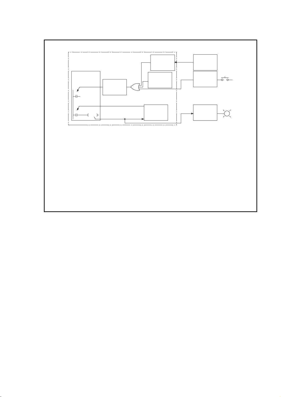
CPU module
CPU (operation
processing area)
3)
DX0
Y20
DY25
Input (X)
device
memory
4)
5)
Remote
input refresh
area
GX
2)
Developer
input area
*3
Output (Y)
device
memory
*1
1)
*2
Network
module
Input
module
Output
module
•When a contact instruction for input is executed:
The CPU module performs a logical OR operation between input data from the input module 1) and
input data in the GX Developer input area 2) or data in the remote input refresh area.
Then, the module stores the result in the input (X) device memory and executes a sequence
program using the stored result as input data 3).
•When a contact instruction for output is executed:
The CPU module reads output data 4) from the output (Y) device memory and executes a sequence
program.
•When the OUT instruction for output is executed:
The CPU module outputs the operation result of the sequence program 5) to the output module and
also stores the result in the output (Y) device memory.
Figure 3.7 I/O data flow in direct mode
*1: The remote input refresh area indicates the area to be used when auto refresh is set to the input (X) in the
CC-Link IE controller network, MELSECNET/H, or CC-Link.
Data in the remote input refresh area will be refreshed automatically during END processing.
*2: Data in the GX Developer input area can be turned on/off by the following operation.
•Test operation by GX Developer
•Writing data from a network module
*3: Data in the output (Y) device memory can be turned on/off by the following operation.
•Test operation by GX Developer
•Refresh via CC-Link IE controller network or MELSECNET/H
•Writing data from an external device using the MC protocol
•Auto refresh via CC-Link
3 - 13
Page 95
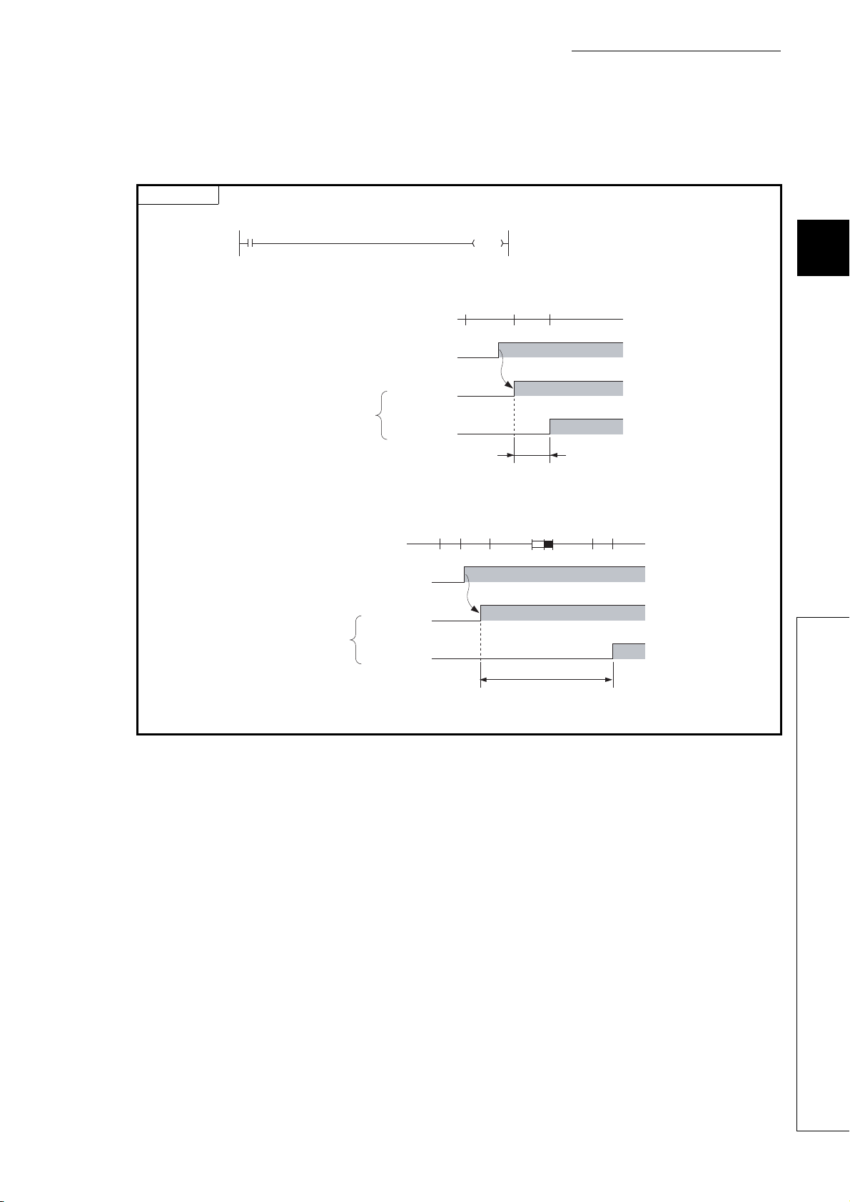
CHAPTER3 CPU MODULE OPERATION
(2) Response delay
An output response which corresponds to the status change in the input module delays for one scan
(maximum) depending on the on timing of an external contact.
Examples
55
DX5
Devices in the
CPU module
Devices in the
CPU module
Figure 3.8 DY5E turns on the earliest
External contact
External contact
DX5
(External
contact)
DY5E
(External
load)
DX5
(External
contact)
DY5E
(External
load)
05556
OFF
OFF
OFF
055 56
ON
OFF
OFF
OFF
A program that turns on the output
DY5E
DY5E when the input DX5 turns on.
ON
ON
ON
Delay time
END 0
ON
Delay time
(Maximum 1 scan)
55 56
ON
3.8.2 Direct mode
1
2
3
4
5
6
7
8
3.8 I/O Processing and Response Delay
Figure 3.9 DY5E turns on the latest
3 - 14
Page 96

CHAPTER4 ASSIGNMENT OF BASE UNIT AND I/O
r
NUMBER
This chapter describes the base unit and I/O number assignment required for the CPU module to
communicate data with I/O modules and/or intelligent function modules.
4.1 Base Unit Assignment
4.1.1 Base mode
Use this mode when assigning the number of available slots to the main base unit and extension base units.
The following two modes are available.
• Auto mode
• Detail mode
(1) Auto mode
Use this mode when assigning the number of slots equal to that on the base unit used.
(2) Detail mode
Use the detail mode when assigning the number of slots for each base unit.
Any number of slots can be assigned irrespective of the actual number of slots on the base unit to be used.
(a) Setting the number of slots greater than the actual one
Slots are occupied by the number of slots set.
The slots after actually used ones are regarded as empty slots.
For example, three slots will be the empty slots when a 5-slot base unit is used and the number of available
slots are set to eight.
Main base unit
Q35B
CPU 0 1 2 3 4 5 6 7
Power supply
module
CPU module
Figure 4.1 Setting the number of slots greater than the actual one
Actual number of slots
Empty
Empty
Number of slots set
Slot numbe
Empty
4 - 1
The number of points for the empty slots will be either value set on the PLC system tab, or on the I/O
assignment tab in the PLC parameter dialog box. (The default is 16 points.)
Page 97

CHAPTER4 ASSIGNMENT OF BASE UNIT AND I/O NUMBER
r
(b) Setting the number of slots smaller than the actual one
Set the smaller number than the actual number of slots when slots with no module mounted need not be
recognized.
For example, four slots from the right end of the base unit will be the prohibited slots when using a 12-slot base
unit and setting the number of available slots to eight. (Mounting a module on a prohibited slot causes
"SP.UNIT LAY ERR.".)
Main base unit
Q312B
Power supply
module
CPU module
CPU 0 1 2 3 4 5 6 7 8 9 10 11
Number of slots set
Figure 4.2 Setting the number of slots smaller than the actual one
4.1.2 Base unit assignment setting
Set base units on the I/O assignment tab of the PLC parameter dialog box.
Actual number of slots
Slot numbe
Prohibited
Prohibited
Prohibited
Prohibited
Mounting a module will result in an error.
1
2
3
4
5
6
7
8
(1)
(4)
(2) (3)
Figure 4.3 I/O assignment setting
(1) Auto/Detail
Select the mode for the base unit assignment either from auto mode or detail mode.
(2) Base model name, Power model name, and Extension cable
Enter the model names of mounted base units, power supply modules, and extension cables to be used within 16
characters for user reference or when printing out parameters.
CPU modules do not use the entered model names.
4.1 Base Unit Assignment
4.1.2 Base unit assignment setting
4 - 2
Page 98

(3) Slots
When "Detail" is set, select the number of slots on the base unit to use from the following.
2 (2 slots), 3 (3 slots), 5 (5 slots), 8 (8 slots), 10 (10 slots), or 12 (12 slots)
(4) 8 Slot Default/12 Slot Default
When "Detail" is set, select either of these items for batch-setting the base units to the specified number of slots.
● In auto mode, when any extension base number is skipped at the setting using the base number setting connector, an
empty extension base cannot be reserved.
To reserve empty extension bases for future extension, select detail mode.
● In detail mode, set the number of slots to all base units used.
Failure to do so may result in incorrect I/O assignment setting.
4 - 3
Page 99

CHAPTER4 ASSIGNMENT OF BASE UNIT AND I/O NUMBER
4.2 I/O Number Assignment
The I/O number indicates addresses used for sequence programs in the following cases.
• Input of on/off data to the CPU module
• Output of on/off data from the CPU module to the external device
(1) Input and output of on/off data
The input (X) is used to input on/off data to the CPU module, and the output (Y) is used to output on/
off data from the CPU module.
(2) I/O number representation
The I/O numbers are represented in hexadecimal.
When a 16-point I/O module is used, the I/O number for each slot will be 16 point-sequence number from
to
"X" and "Y" is prefixed to the I/O number of input modules and the I/O number of output modules, respectively.
F as shown in Figure 4.4.
For the case of input
module
01234
0
000000000
XXXYY
For the case of
output module
1
2
3
4
5
0
6
7
XXXYY
0F0F0F0F00
16 input
points
CPU modulePower supply
Figure 4.4 I/O numbers
1234
F
16 input
points
16 input
points
16 output
points
16 output
points
8
4.2 I/O Number Assignment
4 - 4
Page 100

4.2.1 Concept of I/O number assignment
The CPU module assigns I/O numbers at power on or reset, according to the I/O assignment setting.
(1) I/O number assignment
The Figure 4.5 shows an example of I/O number assignment to base units in the system where the CPU module
is mounted on the main base unit.
Q35B (5 slots occupied)
Number of slot points
Q65B (5 slots occupied)
Assignment order
Number of slot points
Q68B (8 slots occupied)
CPU 0 1 2 3 4
Assignment order
Slot number
I/O number: assign the I/O points of each slot
X00 to 0F
X10 to 1F
X20 to 3F
16 points 16 points 16 points 16 points 16 points
5678 9
90 to AF
B0 to CF
D0 to EF
16 points 16 points 16 points 16 points 16 points
10 11 12 13 14 15 16 17
50 to 8F
X40 to 4F
YF0 to FF
Vacancy (100 to 10F)
I/O number assignment order
Number of I/O points
130 to 14F
150 to 16F
170 to 18F
Y190 to 19F
X 0 to F : Inupt module
Y 0 to F :Output module
0 to F :Intelligent function module
Y180 to 1BF
Y1A0 to 1AF
Assignment order
Number of slot points
Figure 4.5 I/O number assignment example
X110 to 11F
X120 to 12F
16 points 16 points 16 points 16 points 16 points 16 points 16 points 16 points
(a) Assignment order
For the main base unit, the I/O numbers are assigned to the modules from left to right in a
sequential order, starting from 0
H assigned to the module on the right of the CPU module.
For extension base units, the I/O numbers are continued from the last number of the I/O number of
the main base unit.
(b) I/O number of each slot
Each slot on the base unit occupies I/O numbers by the number of I/O points of the mounted
modules.
4 - 5
 Loading...