Feb.1999
MITSUBISHI TRANSISTOR MODULES
QM30E2Y/E3Y-H
MEDIUM POWER SWITCHING USE
INSULATED TYPE
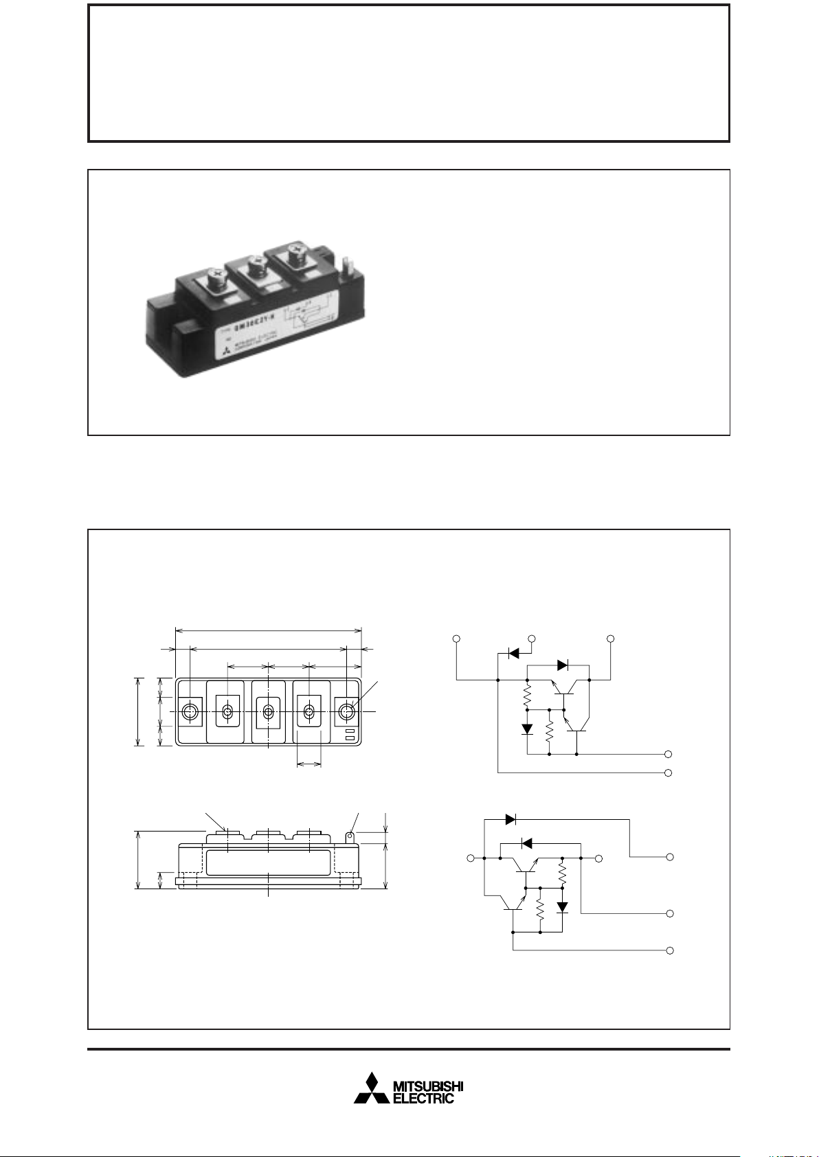
OUTLINE DRAWING & CIRCUIT DIAGRAM Dimensions in mm
APPLICATION
DC chopper, DC motor controllers, Inverters
QM30E2Y/E3Y-H
94
80
(7) (7)
2020 27
φ6.5
12
34
13 10.510.5
E
1
B
1
M5
Tab#110,
t=0.5
6.5
22.5
(8)
31
C
1
A
1
E
1
B
1
E
1
D
1
D
2
D
2
D
1
E
1
E
1
B
1
C
1
K
1
LABEL
(E
2
Y)
(E
3
Y)
• IC Collector current .......................... 30A
• V
CEX Collector-emitter voltage ........... 600V
• h
FE DC current gain............................... 75
• Insulated Type
• UL Recognized
Yellow Card No. E80276 (N)
File No. E80271

Feb.1999
MITSUBISHI TRANSISTOR MODULES
QM30E2Y/E3Y-H
MEDIUM POWER SWITCHING USE
INSULATED TYPE
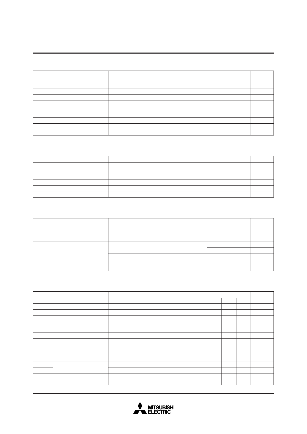
ABSOLUTE MAXIMUM RATINGS (Transistor part including D1, Tj=25°C)
Symbol
V
CEX (SUS)
VCEX
VCBO
VEBO
IC
–IC
PC
IB
–ICSM
Parameter
Collector-emitter voltage
Collector-emitter voltage
Collector-base voltage
Emitter-base voltage
Collector current
Collector reverse current
Collector dissipation
Base current
Surge collector reverse current
(forward diode current)
Conditions
I
C=1A, VEB=2V
V
EB=2V
Emitter open
Collector open
DC
DC (forward diode current)
T
C=25°C
DC
Peak value of one cycle of 60Hz (half wave)
Ratings
600
600
600
7
30
30
250
1.8
300
Unit
V
V
V
V
A
A
W
A
A
ABSOLUTE MAXIMUM RATINGS (Diode part (D2), Tj=25°C)
Symbol
V
RRM
VRSM
VR (DC)
IDC
IFSM
I
2
t
Parameter
Repetitive peak reverse voltage
Non-repetitive peak reverse voltage
DC reverse voltage
DC current
Surge (non-repetitive) forward current
I
2
t
for fusing
Conditions
DC circuit, resistive, inductive load
Peak value of one cycle of 60Hz (half wave)
Value for one cycle of surge current
Ratings
600
720
480
30
600
1.5 × 10
3
Unit
V
V
V
A
A
A
2
s
ABSOLUTE MAXIMUM RATINGS (Common)
Symbol
T
j
Tstg
Viso
—
—
Parameter
Junction temperature
Storage temperature
Isolation voltage
Mounting torque
Weight
Conditions
Charged part to case, AC for 1 minute
Main terminal screw M5
Mounting screw M6
Typical value
Ratings
–40~150
–40~125
2500
1.47~1.96
15~20
1.96~2.94
20~30
210
Unit
°C
°C
V
N·m
kg·cm
N·m
kg·cm
g
Unit
mA
mA
mA
V
V
V
—
µs
µs
µs
°C/W
°C/W
°C/W
Limits
Min.
—
—
—
—
—
—
75/100
—
—
—
—
—
—
Symbol
I
CEX
ICBO
IEBO
VCE (sat)
VBE (sat)
–VCEO
hFE
ton
ts
tf
Rth (j-c) Q
Rth (j-c) R
Rth (c-f)
Parameter
Collector cutoff current
Collector cutoff current
Emitter cutoff current
Collector-emitter saturation voltage
Base-emitter saturation voltage
Collector-emitter reverse voltage
DC current gain
Switching time
Thermal resistance
(junction to case)
Contact thermal resistance
(case to fin)
Test conditions
V
CE=600V, VEB=2V
V
CB=600V, Emitter open
V
EB=7V
I
C=30A, IB=0.4A
–I
C=30A (diode forward voltage)
I
C=30A, VCE=2V/5V
V
CC=300V, IC=30A, IB1=–IB2=0.6A
Transistor part
Diode part
Conductive grease applied
Typ.
—
—
—
—
—
—
—
—
—
—
—
—
—
Max.
1.0
1.0
200
2.0
2.5
1.85
—
1.5
12
3.0
0.5
2.0
0.15
ELECTRICAL CHARACTERISTICS (Transistor part including D1, Tj=25°C)
 Loading...