


Channel Isolated Analog-Digital Converter Module/
Channel Isolated Analog-Digital Converter Module
(With Signal Conditioning Function)
User's Manual
-Q68AD-G
-Q66AD-DG
-GX Configurator-AD (SW2D5C-QADU-E)

SAFETY PRECAUTIONS
(Read these precautions before using this product.)
Before using this product, please read this manual and the relevant manuals carefully and pay full attention
to safety to handle the product correctly.
In this manual, the safety precautions are classified into two levels: " WARNING" and " CAUTION".
WARNING
CAUTION
Under some circumstances, failure to observe the precautions given under " CAUTION" may lead to
serious consequences.
Observe the precautions of both levels because they are important for personal and system safety.
Make sure that the end users read this manual and then keep the manual in a safe place for future
reference.
Indicates that incorrect handling may cause hazardous conditions,
resulting in death or severe injury.
Indicates that incorrect handling may cause hazardous conditions,
resulting in minor or moderate injury or property damage.
[Design Precaution]
WARNING
Do not write any data to the "system area" or "write-protect area" of the buffer memory areas in
the intelligent function module. Also, do not use any "prohibited to use" signals as an output
signal to an intelligent function module from the programmable controller CPU.
Doing so may cause malfunction of the programmable controller system.
CAUTION
Do not bunch the control wires or communication cables with the main circuit or power wires, or
install them close to each other.
They should be installed 100mm or more from each other.
Not doing so could result in noise that may cause malfunction.
A - 1
[Installation Precautions]
CAUTION
Use the programmable controller in an environment that meets the general specifications
contained in the user's manual of the CPU module to use.
Using this programmable controller in an environment outside the range of the general
specifications may cause electric shock, fire, malfunction, and damage to or deterioration of the
product.
While pressing the installation lever located at the bottom of module, insert the module fixing tab
into the fixing hole in the base unit until it stops. Then, securely mount the module with the fixing
hole as a supporting point.
For the Q66AD-DG, secure the module with fixing brackets after installation to the base unit.
When using the Q68AD-G in an environment where they are frequent vibrations, screw the module
to the base unit after installation.
Tighten the screws within the range of specified torque.
If the screws are loose, it may cause the module to fallout, short circuits, or malfunction.
If the screws are tightened too much, it may cause damage to the screw and/or the module,
resulting in fallout, short circuits or malfunction.
Be sure to shut off all phases of the external power supply used by the system before mounting or
removing the module.
Not doing so may cause damage to the module.
In the system where a CPU module supporting the online module change is used and on the
MELSECNET/H remote I/O stations, modules can be replaced online (during energizing).
However, there are some restrictions on replaceable modules and the replacement procedures
are predetermined for each module.
For details, refer to the chapter of the online module change in this manual.
Do not directly touch the conductive area or electronic components of the module.
Doing so may cause malfunction or failure in the module.
A - 2
[Wiring Precautions]
CAUTION
Individually ground the FG terminal of the programmable controller with a ground resistance of
100Ω or less.
Not doing so can cause an electric shock or malfunction.
When turning on the power and operating the module after wiring is completed, always attach the
terminal cover that comes with the product.
There is a risk of electric shock if the terminal cover is not attached.
Tighten the terminal screws within the range of specified torque.
If the terminal screws are loose, it may result in short circuits or malfunction.
If the terminal screws are tightened too much, it may cause damage to the screw and/or the
module, resulting in short circuits or malfunction.
Be careful not to let foreign matter such as sawdust or wire chips get inside the module.
They may cause fires, failure or malfunction.
The top surface of the module is covered with protective film to prevent foreign objects such as
cable offcuts from entering the module when wiring.
Do not remove this film until the wiring is complete.
Before operating the system, be sure to remove the film to provide adequate ventilation.
A - 3
[Starting and Maintenance Precautions]
CAUTION
Do not disassemble or modify the modules.
Doing so could cause failure, malfunction injury or fire.
Be sure to shut off all phases of the external power supply used by the system before mounting or
removing the module.
Not doing so may cause failure or malfunction of the module.
In the system where a CPU module supporting the online module change is used and on the
MELSECNET/H remote I/O stations, modules can be replaced online (during energizing).
However, there are some restrictions on replaceable modules and the replacement procedures
are predetermined for each module.
For details, refer to the chapter of the online module change in this manual.
Do not install/remove the module to/from the base unit more than 50 times after the first use of the
product. (IEC 61131-2 compliant)
Failure to do so may cause malfunction.
Do not touch the connector while the power is on.
Doing so may cause malfunction.
Be sure to shut off all phases of the external power supply before cleaning or retightening the
terminal screws or module fixing screws.
Not doing so may cause failure or malfunction of the module.
If the screws are loose, it may cause the module to fallout, short circuits, or malfunction.
If the screws are tightened too much, it may cause damages to the screws and/or the module,
resulting in the module falling out, short circuits or malfunction.
Always make sure to touch the grounded metal to discharge the electricity charged in the body,
etc., before touching the module.
Failure to do so may cause a failure or malfunctions of the module.
[Disposal Precautions]
CAUTION
When disposing of this product, treat it as industrial waste.
A - 4

CONDITIONS OF USE FOR THE PRODUCT
(1) Mitsubishi programmable controller ("the PRODUCT") shall be used in conditions;
i) where any problem, fault or failure occurring in the PRODUCT, if any, shall not lead to any major
or serious accident; and
ii) where the backup and fail-safe function are systematically or automatically provided outside of
the PRODUCT for the case of any problem, fault or failure occurring in the PRODUCT.
(2) The PRODUCT has been designed and manufactured for the purpose of being used in general
industries.
MITSUBISHI SHALL HAVE NO RESPONSIBILITY OR LIABILITY (INCLUDING, BUT NOT
LIMITED TO ANY AND ALL RESPONSIBILITY OR LIABILITY BASED ON CONTRACT,
WARRANTY, TORT, PRODUCT LIABILITY) FOR ANY INJURY OR DEATH TO PERSONS OR
LOSS OR DAMAGE TO PROPERTY CAUSED BY the PRODUCT THAT ARE OPERATED OR
USED IN APPLICATION NOT INTENDED OR EXCLUDED BY INSTRUCTIONS, PRECAUTIONS,
OR WARNING CONTAINED IN MITSUBISHI'S USER, INSTRUCTION AND/OR SAFETY
MANUALS, TECHNICAL BULLETINS AND GUIDELINES FOR the PRODUCT.
("Prohibited Application")
Prohibited Applications include, but not limited to, the use of the PRODUCT in;
• Nuclear Power Plants and any other power plants operated by Power companies, and/or any
other cases in which the public could be affected if any problem or fault occurs in the PRODUCT.
• Railway companies or Public service purposes, and/or any other cases in which establishment of
a special quality assurance system is required by the Purchaser or End User.
• Aircraft or Aerospace, Medical applications, Train equipment, transport equipment such as
Elevator and Escalator, Incineration and Fuel devices, Vehicles, Manned transportation,
Equipment for Recreation and Amusement, and Safety devices, handling of Nuclear or
Hazardous Materials or Chemicals, Mining and Drilling, and/or other applications where there is a
significant risk of injury to the public or property.
Notwithstanding the above, restrictions Mitsubishi may in its sole discretion, authorize use of the
PRODUCT in one or more of the Prohibited Applications, provided that the usage of the PRODUCT
is limited only for the specific applications agreed to by Mitsubishi and provided further that no
special quality assurance or fail-safe, redundant or other safety features which exceed the general
specifications of the PRODUCTs are required. For details, please contact the Mitsubishi
representative in your region.
A - 5
REVISIONS
Correction
Correction
Addition
Correction
Correction
Addition
Correction
Addition
Correction
* The manual number is given on the bottom left of the back cover.
Print Date *Manual Number Revision
Oct., 2006 SH (NA)-080647ENG-A First edition
Jan., 2007 SH(NA)-080647ENG-B
Section 3.3.2, 3.4.12, 4.6.2, 6.3.1, 6.3.2, 6.5.1, 6.5.2
Jan., 2008 SH(NA)-080647ENG-C
SAFETY PRECAUTIONS, About the Generic Terms and Abbreviations, Section
1.1, Section 2.1, Section 2.3, Section 3.2.1, Section 3.4.1, Section 4.1, Section
4.4.2, Section 4.6.1, Section 4.6.2, Section 5.2.1, Section 5.2.2, Section 5.3.2,
Section 5.3.3, Section 5.6.1, Section 5.6.4, Section 5.6.5, Section 7.3.3, Section
7.3.5, Section 8.1, Appendix 1, Appendix 1.1, Appendix 1.2, Appendix 1.3
Section 2.2
May, 2008 SH(NA)-080647ENG-D
SAFETY PRECAUTIONS, Compliance with the EMC and Low Voltage Directives, About the Generic Terms and Abbreviations, Section 2.1, 2.3, Section
3.1.1, 3.2.1, 3.2.4, Section 4.1, 4.3, Section 5.2.1, 5.2.2, 5.3.1, 5.3.2, 5.3.3,
Chapter 7, Section 7.1
Oct., 2008 SH(NA)-080647ENG-E
Section 2.1, Section 3.1.1, 3.1.2, 3.2, 3.2.1, 3.2.3, 3.2.6, 3.3.2, 3.4.1, 3.4.2,
3.4.4, 3.4.7, 3.4.9, 3.4.11, 3.4.12, 3.4.13, 3.4.22, Section 4.3, 4.5, Section 5.1,
5.4, Section 8.1, 8.2.4, 8.2.6, Appendix 1.1, 1.2, 1.3
Sep., 2011 SH(NA)-080647ENG-F
Feb., 2012 SH(NA)-080647ENG-G
Appendix 2
SAFETY PRECAUTIONS, COMPLIANCE WITH THE EMC AND LOW VOLTAGE DIRECTIVES, Section 4.6.1, 4.6.2, 4.6.3, 6.2.1, 6.2.2, 6.2.3, 6.3, 6.3.1,
6.3.2, 6.4, 6.4.1, 6.4.2, 6.4.3, 6.5, 6.5.1, 6.5.2
CONDITIONS OF USE FOR THE PRODUCT
SAFETY PRECAUTIONS, COMPLIANCE WITH THE EMC AND LOW VOLTAGE DIRECTIVES, Section 1.1, 2.1 to 2.3, 3.1.1, 3.1.2, 3.2, 3.2.1, 3.2.3, 3.2.4,
3.2.6, 3.3.2, 3.4.1, 3.4.2, 3.4.4, 3.4.5, 3.4.7, 3.4.10, 3.4.15 to 3.4.17, 3.4.19,
3.4.21, 3.4.22, 3.4.25, 4.1, 4.1.1, 4.3, 4.4.2, 4.5, 4.6.1, 4.6.2, 5.2.1, 5.2.2, 5.3.1,
5.3.3, 5.4, 5.5, 5.6.1 to 5.6.3, 6.2.1, 6.2.2, 6.3, 6.3.1, 6.4.1, 6.4.2, 6.5, 6.5.1,
Chapter 7, 7.1, 7.2, 7.3.1 to 7.3.6, 7.5, 8.1, 8.2.4, 8.2.6, Appendix 2, Appendix 3
A - 6

Print Date *Manual Number Revision
Correction
Correction
Dec., 2015 SH(NA)-080647ENG-H
SAFETY PRECAUTIONS, MANUALS, COMPLIANCE WITH THE EMC, LOW
VOLTAGE, AND MACHINERY DIRECTIVES, GENERIC TERMS AND ABBREVIATIONS, Section 2.1, 3.1, 3.1.1, 3.2, 3.3.2, 3.4.2, 3.4.4, 4.4.2, 4.6.2, 5.2.1,
5.2.2, 6.3.2, 6.4.2, 6.5.1, 6.5.2, 8.1, 8.2.1, 8.2.4, Appendix 2
Jul., 2017 SH(NA)-080647ENG-I
INTRODUCTION, COMPLIANCE WITH THE EMC, LOW VOLTAGE, AND
MACHINERY DIRECTIVES, GENERIC TERMS AND ABBREVIATIONS, Section 2.1, 2.3, 4.3, 4.4.2, 4.4.3, 6.2.1, 6.4.1, Appendix 3
Japanese Manual Version SH-080645-L
This manual confers no industrial property rights or any rights of any other kind, nor does it confer any patent
licenses. Mitsubishi Electric Corporation cannot be held responsible for any problems involving industrial
property rights which may occur as a result of using the contents noted in this manual.
© 2006 MITSUBISHI ELECTRIC CORPORATION
A - 7

INTRODUCTION
Thank you for purchasing the Mitsubishi Electric MELSEC-Q series programmable controllers.
Before using the equipment, please read this manual carefully to develop full familiarity with the functions
and performance of the Q series programmable controller you have purchased, so as to ensure
correct use.
Please forward a copy of this manual to the end user.
CONTENTS
SAFETY PRECAUTIONS .................................................................................................................................A - 1
CONDITIONS OF USE FOR THE PRODUCT..................................................................................................A - 5
REVISIONS.......................................................................................................................................................A - 6
INTRODUCTION...............................................................................................................................................A - 8
CONTENTS ......................................................................................................................................................A - 8
MANUALS....................................................................................................................................................... A - 12
COMPLIANCE WITH THE EMC, LOW VOLTAGE, AND MACHINERY DIRECTIVES ..................................A - 12
GENERIC TERMS AND ABBREVIATIONS....................................................................................................A - 13
PACKING LIST ...............................................................................................................................................A - 14
1 OVERVIEW 1 - 1 to 1 - 3
1.1 Features........................................................................................................................................... 1 - 1
2 SYSTEM CONFIGURATION 2 - 1 to 2 - 6
2.1 Applicable Systems ......................................................................................................................... 2 - 1
2.2 Precautions on System Configuration ............................................................................................. 2 - 3
2.3 How to Check the Function Version, Serial No., and Software Version .......................................... 2 - 4
3 SPECIFICATIONS 3 - 1 to 3 - 75
3.1 Performance Specifications ............................................................................................................. 3 - 1
3.1.1 Performance specifications list ............................................................................................... 3 - 1
3.1.2 I/O conversion characteristic .................................................................................................. 3 - 5
3.1.3 Accuracy ............................................................................................................................... 3 - 12
3.2 Function List .................................................................................................................................. 3 - 13
3.2.1 A/D conversion methods ...................................................................................................... 3 - 15
3.2.2 Maximum and minimum values hold function....................................................................... 3 - 18
3.2.3 Input signal error detection function ..................................................................................... 3 - 18
3.2.4 Warning output function........................................................................................................ 3 - 25
3.2.5 Conversion starting time setting function (Q66AD-DG only) ................................................ 3 - 29
3.2.6 Scaling Function ................................................................................................................... 3 - 30
3.3 I/O Signals for the Programmable Controller CPU ........................................................................ 3 - 33
3.3.1 List of I/O signals .................................................................................................................. 3 - 33
3.3.2 Details of I/O signals............................................................................................................. 3 - 35
3.4 Buffer Memory ............................................................................................................................... 3 - 43
3.4.1 Buffer memory assignment...................................................................................................3 - 43
A - 8

3.4.2 A/D conversion enable/disable setting (Un\G0).................................................................... 3 - 55
3.4.3 CH[ ] average time/average number of times/moving average/time constant settings
(Un\G1 to Un\G8) ................................................................................................................. 3 - 56
3.4.4 A/D conversion completed flag (Un\G10) ............................................................................. 3 - 57
3.4.5 CH[ ] digital output value (Un\G11 to Un\G18) ..................................................................... 3 - 58
3.4.6 Write data error code (Un\G19) ............................................................................................ 3 - 59
3.4.7 Setting range (Un\G20, Un\G21) .......................................................................................... 3 - 59
3.4.8 Offset/gain setting mode offset/gain specification (Un\G22, Un\G23) .................................. 3 - 60
3.4.9 Averaging process specification (Un\G24, Un\G25))............................................................ 3 - 61
3.4.10 CH[ ] maximum value/minimum value storage area (Un\G30 to Un\G45)............................ 3 - 62
3.4.11 Input signal error detection extended/input signal error detection setting (Un\G47) ............ 3 - 62
3.4.12 Warning output settings (Un\G48) ........................................................................................ 3 - 64
3.4.13 Input signal error detection flag (Un\G49) ............................................................................ 3 - 65
3.4.14 Warning output flag (Un\G50,Un\51) .................................................................................... 3 - 66
3.4.15 Scaling enable/disable setting (Un\G53) .............................................................................. 3 - 66
3.4.16 CH[ ] scaling value storage area (Un\G54 to Un\G61) ......................................................... 3 - 67
3.4.17 CH[ ] scaling upper / lower limit value (Un\G62 to Un\G77) ................................................. 3 - 67
3.4.18 CH[ ] conversion starting time setting (for 2-wire transmitter) (Un\G78 to Un\G83)
(Q66AD-DG only) .................................................................................................................3 - 67
3.4.19 CH[ ] process alarm upper/lower limit value (Un\G86 to Un\G117) ...................................... 3 - 68
3.4.20 CH[ ] rate alarm warning detection period (Un\G118 to Un\G125)....................................... 3 - 69
3.4.21 CH[ ] rate alarm upper/lower limit value (Un\G126 to Un\G141) .......................................... 3 - 70
3.4.22 CH[ ] input signal error detection setting value/CH[ ] Input signal error detection lower
limit setting value (Un\G142 to Un\G149)
CH[ ] Input signal error detection upper limit setting value (Un\G150 to Un\G157).............. 3 - 71
3.4.23 Mode switching setting (Un\G158, Un\G159) ....................................................................... 3 - 74
3.4.24 Save data classification setting (Un\G200) (Q68AD-G only) ................................................ 3 - 74
3.4.25 Factory default and User range settings offset/gain value (Un\G202 to Un\G233) .............. 3 - 75
4 SETUP AND PROCEDURES BEFORE OPERATION 4 - 1 to 4 - 24
4.1 Handling Precautions....................................................................................................................... 4 - 1
4.1.1 Attaching a module fixing bracket (Q66AD-DG only) ............................................................. 4 - 2
4.2 Setup and Procedures before Operation ......................................................................................... 4 - 3
4.3 Part Names...................................................................................................................................... 4 - 4
4.4 Wiring............................................................................................................................................... 4 - 7
4.4.1 Wiring precautions.................................................................................................................. 4 - 7
4.4.2 External wiring ........................................................................................................................ 4 - 8
4.4.3 Connector/terminal block converter module ......................................................................... 4 - 11
4.5 Intelligent Function Module Switch Setting .................................................................................... 4 - 12
4.6 Offset/Gain Settings....................................................................................................................... 4 - 14
4.6.1 Offset/gain settings (Q68AD-G)............................................................................................ 4 - 15
4.6.2 Offset/gain settings (Q66AD-DG) ......................................................................................... 4 - 19
4.6.3 A/D conversion value storage during offset/gain setting ...................................................... 4 - 24
5 UTILITY PACKAGE (GX Configurator-AD) 5 - 1 to 5 - 33
5.1 Utility Package Functions ................................................................................................................ 5 - 1
5.2 Installing and Uninstalling the Utility Package ................................................................................. 5 - 2
A - 9

5.2.1 Handling precautions.............................................................................................................. 5 - 2
5.2.2 Operating environment ........................................................................................................... 5 - 4
5.3 Utility Package Operation ................................................................................................................ 5 - 6
5.3.1 Common utility package operations ....................................................................................... 5 - 6
5.3.2 Operation overview................................................................................................................. 5 - 9
5.3.3 Starting the intelligent function module utility ....................................................................... 5 - 11
5.4 Initial Setting .................................................................................................................................. 5 - 14
5.5 Auto Refresh Setting...................................................................................................................... 5 - 16
5.6 Monitoring/Test .............................................................................................................................. 5 - 18
5.6.1 Monitor/test window .............................................................................................................. 5 - 18
5.6.2 Offset/gain setting operation................................................................................................. 5 - 21
5.6.3 Confirmation of conversion characteristic............................................................................. 5 - 23
5.6.4 Pass data (Q68AD-G) .......................................................................................................... 5 - 25
5.6.5 Pass data (Q66AD-DG) ........................................................................................................ 5 - 27
5.7 FB Conversion of Initial Setting/Auto Refresh Setting ................................................................... 5 - 28
5.8 Usage of FB................................................................................................................................... 5 - 30
5.8.1 Outline .................................................................................................................................. 5 - 30
5.8.2 Paste an FB to a sequence program .................................................................................... 5 - 32
5.8.3 Convert (compile) a sequence program ............................................................................... 5 - 33
6 PROGRAMMING 6 - 1 to 6 - 38
6.1 Programming Procedure.................................................................................................................. 6 - 1
6.2 For Use in Normal System Configuration (Q68AD-G) ..................................................................... 6 - 2
6.2.1 Before creating a program ...................................................................................................... 6 - 3
6.2.2 Programming example using the utility package .................................................................... 6 - 5
6.2.3 Programming example without using the utility package........................................................ 6 - 8
6.3 For Use in Remote I/O Network (Q68AD-G) ................................................................................. 6 - 11
6.3.1 Programming example using the utility package .................................................................. 6 - 14
6.3.2 Programming example without using the utility package...................................................... 6 - 17
6.4 For Use in Normal System Configuration (Q66AD-DG)................................................................. 6 - 21
6.4.1 Before creating a program .................................................................................................... 6 - 22
6.4.2 Programming example using the utility package .................................................................. 6 - 24
6.4.3 Programming example without using the utility package...................................................... 6 - 27
6.5 For Use in Remote I/O Network (Q66AD-DG) ............................................................................... 6 - 30
6.5.1 Programming example using the utility package .................................................................. 6 - 32
6.5.2 Programming example without using the utility package...................................................... 6 - 35
7 ONLINE MODULE CHANGE 7 - 1 to 7 - 38
7.1 Online Module Change Conditions .................................................................................................. 7 - 2
7.2 Online Module Change Operations ................................................................................................. 7 - 3
7.3 Online Module Change Procedure .................................................................................................. 7 - 4
7.3.1 When industrial shipment setting is used and initial setting was made with
GX Configurator-AD ............................................................................................................... 7 - 5
7.3.2 When industrial shipment setting is used and initial setting was made with
sequence program................................................................................................................7 - 10
A - 10

7.3.3 When user range setting is used and initial setting was made with GX Configurator-AD
(other system is available).................................................................................................... 7 - 15
7.3.4 When user range setting is used and initial setting was made with GX Configurator-AD
(other system is unavailable)................................................................................................ 7 - 20
7.3.5 When user range setting is used and initial setting was made with sequence program
(other system is available).................................................................................................... 7 - 26
7.3.6 When user range setting is used and initial setting was made with sequence program
(other system is unavailable)................................................................................................ 7 - 31
7.4 Range Reference Table................................................................................................................. 7 - 37
7.5 Precautions for Online Module Change.........................................................................................7 - 38
8 TROUBLESHOOTING 8 - 1 to 8 - 8
8.1 Error Code List................................................................................................................................ 8 - 1
8.2 Troubleshooting ............................................................................................................................... 8 - 5
8.2.1 When the "RUN" LED is flashing or turned off ....................................................................... 8 - 5
8.2.2 When the "ERR." LED is on or flashing.................................................................................. 8 - 5
8.2.3 When the "ALM" LED is on or flashing ................................................................................... 8 - 5
8.2.4 When the digital output values cannot be read ...................................................................... 8 - 6
8.2.5 When A/D conversion completed flag does not turn ON during use in normal mode ............ 8 - 7
8.2.6 Checking the A/D converter module status using GX Developer system monitor.................. 8 - 7
APPENDIX App - 1 to App - 17
Appendix 1 Dedicated Instruction List and Available Devices.................................................................. App- 1
Appendix 1.1G(P).OFFGAN .................................................................................................................App- 2
Appendix 1.2G(P).OGLOAD ................................................................................................................. App- 4
Appendix 1.3G(P).OGSTOR................................................................................................................. App- 8
Appendix 2 Functions Added or Changed Due to Version Upgrade ......................................................App- 13
Appendix 3 External Dimensions............................................................................................................ App- 17
INDEX Index - 1 to Index - 2
A - 11
MANUALS
Remark
Relevant Manuals
The manuals related to this product are listed below.
Please place an order as needed.
Manual name
GX Developer Version 8 Operating Manual
Operating methods of GX Developer, such as programming, printing, monitoring, and debugging
(Sold separately)
GX Developer Version 8 Operating Manual (Function Block)
Operating methods of GX Developer, such as creating and printing function blocks (Sold separately)
GX Works2 Version1 Operating Manual (Common)
System configuration, parameter settings, and online operations (common to Simple project and Structured
project) of GX Works2 (Sold separately)
GX Works2 Version1 Operating Manual (Intelligent Function Module)
Operating methods of the intelligent function module of GX Works2, such as parameter settings, monitoring,
and predefined protocol support function (Sold separately)
Printed manuals are available separately. Please place an order with the manual
number (model code) in the table above.
COMPLIANCE WITH THE EMC, LOW VOLTAGE, AND MACHINERY DIRECTIVES
Manual number
(model code)
SH-080373E
(13JU41)
SH-080376E
(13JU44)
SH-080779ENG
(13JU63)
SH-080921ENG
(13JU69)
(1) Method of ensuring compliance
To ensure that Mitsubishi Electric programmable controllers maintain EMC and Low
Voltage Directives when incorporated into other machinery or equipment, certain
measures may be necessary. Please refer to one of the following manuals.
• QCPU User's Manual (Hardware Design, Maintenance and Inspection)
• Safety Guidelines (This manual is included with the CPU module or head module.)
The CE mark on the side of the programmable controller indicates compliance with
EMC and Low Voltage Directives.
(2) Additional measures
No additional measures are necessary for the compliance of this product with EMC
and Low Voltage Directives.
A - 12

GENERIC TERMS AND ABBREVIATIONS
Unless otherwise specified, this manual uses the following general terms and
abbreviations.
General term/Abbreviation Description
A/D converter module A generic term for the Q68AD-G and Q66AD-DG
DOS/V personal computer
GX Developer
GX Works2
GX Configurator-AD
QCPU (Q mode)
Process CPU A generic term for the Q02PHCPU, Q06PHCPU, Q12PHCPU and Q25PHCPU
Redundant CPU Generic term for Q12PRHCPU and Q25PRHCPU.
Personal computer A generic term for DOS/V personal computers
Industrial shipment setting
FB The abbreviation for function block
An IBM PC/AT or compatible computer with DOS/V
The product name of the software package for the MLSEC programmable controllers
The abbreviation for the analog-digital converter module setting and monitor tool GX Configurator-AD (SW2D5C-QADU-E)
A generic term for the Q00JCPU, Q00CPU, Q01CPU, Q02CPU, Q02HCPU, Q06HCPU, Q12HCPU,
Q25HCPU, Q02PHCPU, Q06PHCPU, Q12PHCPU, Q25PHCPU, Q12PRHCPU, Q25PRHCPU,
Q00UJCPU, Q00UCPU, Q01UCPU, Q02UCPU, Q03UDCPU, Q04UDHCPU, Q06UDHCPU,
Q10UDHCPU, Q13UDHCPU, Q20UDHCPU, Q26UDHCPU, Q03UDVCPU, Q04UDVCPU,
Q06UDVCPU, Q13UDVCPU, Q26UDVCPU, Q03UDECPU, Q04UDEHCPU, Q06UDEHCPU,
Q10UDEHCPU, Q13UDEHCPU, Q20UDEHCPU, Q26UDEHCPU, Q50UDEHCPU, and
Q100UDEHCPU.
A generic term for analog input ranges 0 to 10V, 0 to 5V, 1 to 5V, -10 to 10V, 0 to 20mA, and 4 to
20mA
A - 13

PACKING LIST
The product package contains the following.
Model Product Quantity
Q68AD-G Type Q68AD-G Channel Isolated Analog-Digital Converter Module 1
Type Q66AD-DG Channel Isolated Analog-Digital Converter Module (with Signal
Q66AD-DG
SW2D5C-QADU-E GX Configurator-AD Version 2 (1-license product)(CD-ROM) 1
SW2D5C-QADU-EA GX Configurator-AD Version 2 (Multiple-license product)(CD-ROM) 1
Conditioning Function)
FG terminal L-Shaped metal fitting 1
1
A - 14

1
OVERVIEW
1 OVERVIEW
This User's Manual describes the specifications, handling and programming methods for
the type Q68AD-G channel isolated analog-digital converter module (hereinafter referred
to as the Q68AD-G) and type Q66AD-DG channel isolated analog-digital converter
module (with signal conditioning function) (hereinafter referred to as the Q66AD-DG),
which are used with the MELSEC-Q series CPU modules.
The Q66AD-DG is exclusively used for current input.
In this manual, the Q68AD-G and Q66AD-DG are collectively referred to as the A/D
converter modules.
1.1 Features
(1) Channel isolated
The channels are isolated.
The Q66AD-DG is also isolated between the external power supply and channels.
(2) Multi-channel analog input is available.
1
2
SYSTEM
3
4
OVERVIEW
CONFIGURATION
SPECIFICATIONS
(a) By using a single Q68AD-G, analog voltage or current inputs of 8 channels are
available.
(b) A single Q66AD-DG allows connection of 2-wire transmitters of 6 channels.
It has an input range for analog current, in addition to connections to 2-wire
transmitters.
(3) Power supply to 2-wire transmitter (Q66AD-DG only)
Supplying power to the 2-wire transmitter, the Q66AD-DG does not require the power
supply for the 2-wire transmitter.
Supply power can be switched ON/OFF channel-by-channel by the A/D conversion
enable/disable setting.
(4) Module protection provided by short-circuit protection circuit
(Q66AD-DG only)
If an excessive current flows into the module due to a short circuit of the wiring, the
short-circuit protection circuit limits the current to within 25 to 35mA, protecting the
module.
(5) Analog input check by check terminals (Q66AD-DG only)
Measurement of a voltage at the check terminals allows the mA of the 2-wire
transmitter output to be checked without the wiring being disconnected.
SETUP AND
PROCEDURES
BEFORE OPERATION
5
UTILITY PACKAGE
(GX CONFIGURATOR-
AD)
6
PROGRAMMING
7
1.1 Features
ONLINE MODULE
CHANGE
8
TROUBLESHOOTING
1 - 1

1
OVERVIEW
(6) High accuracy
The reference accuracy *1 is as high as ±0.1% and the temperature coefficient*2 is as high
as ±71.4ppm/°C.
*1 Accuracy of offset/gain setting at ambient temperature
*2 Accuracy per temperature change of 1°C
Example) Accuracy when the temperature varies from 25 to 30°C
0.1% (reference accuracy) + 0.00714 %/°C (temperature coefficient) 5°C
(temperature variation difference) = 0.1357%
(7) Changing the input range
The input range*3 can easily be set from the GX Developer.
*3 Input range refers to the type of offset/gain settings. The most frequently used range is set as the
default but the user can also set the offset/gain.
(8) A/D conversion system
There are the following five A/D conversion systems.
(a) Sampling processing
Analog input values are converted into digital values one by one on a channel
basis and the digital output value is output at every conversion.
(b) Averaging processing
1) Time averaging
A/D conversion is averaged in terms of time on a channel basis and a digital
average value is output.
2) Count averaging
A/D conversion is averaged in terms of count on a channel basis and a digital
average value is output.
3) Move averaging
The specified number of digital output values measured per sampling time are
averaged.
(c) Primary delay filter
A digital output value is smoothed according to the preset time constant.
*1 Refer to Section 3.2.1 for the details of the A/D conversion system.
*1
1 - 2
(9) Input signal error detection function
The voltage/current outside the setting range is detected.
(10)Warning output
There are the following two warning outputs.
(a) Process alarm
A warning is output if a digital output value falls outside the setting range.
(b) Rate alarm
A warning is output if the varying rate of a digital output value falls outside the
preset varying rate range.
*1 Refer to Section 3.2.4 for details on warning output.
1.1 Features
*1

1
OVERVIEW
(11)Scaling function
(12)Online module change
(13)Offset/gain setting
(14)Easy settings using GX Configurator-AD
A/D conversion values can be converted to percentage values (%) in the preset range
and be loaded into the buffer memory. This function can reduce the time required for
programming. (Refer to Section 3.2.6.)
Furthermore, the following operations can be processed by using sequence programs. (Note that these operations are possible for the modules of the same model
only.) (Refer to Chapter7.)
• Transferring the offset/gain set values to the replacement A/D converter module
• Transferring the offset/and gain set values to another A/D converter module
mounted on the other slot
GX Configurator-AD, dedicated instruction (G(P).OFFGAN) or mode switching setting
allows a shift to the offset/gain setting mode easily.
Using GX Configurator-AD which is sold separately, sequence programs can be
reduced since settings of the A/D converter module can be made on the window.
Also, the set status or operating status of the module can be checked easily.
*1
can be created automatically from the set intelligent function module parame-
A FB
ter, and can be used in sequence programs.
*1 FB is the function for making a circuit block used in a sequence program repeatedly a part (FB) to
use it in the sequence program.
This function can improve the efficiency of program development and minimize program bugs to
improve program qualities.
1
2
SYSTEM
3
4
SETUP AND
PROCEDURES
5
OVERVIEW
CONFIGURATION
SPECIFICATIONS
BEFORE OPERATION
For the details of FB, refer to "GX Developer Version 8 Operating Manual (Function
Block)."
UTILITY PACKAGE
(GX CONFIGURATOR-
AD)
6
PROGRAMMING
7
ONLINE MODULE
CHANGE
8
1.1 Features
TROUBLESHOOTING
1 - 3

2
Remark
SYSTEM CONFIGURATION
2 SYSTEM CONFIGURATION
This chapter explains the system configuration of the A/D converter module.
2.1 Applicable Systems
This section describes the applicable systems.
(1) Applicable modules and base units, and No. of modules
(a) When mounted with a CPU module
For the CPU modules, the number of modules, and base units applicable to the A/
D converter module, refer to the following.
• User's Manual (Hardware Design, Maintenance and Inspection) for the CPU
module used
To use the A/D converter module with a C Controller module, refer to the user's
manual for the C Controller module.
(b) Mounting to a MELSECNET/H remote I/O station
For the number of modules and base units applicable to the A/D converter module, refer to the following.
• Q Corresponding MELSECNET/H Network System Reference Manual
(Remote I/O network)
(2) Support of the multiple CPU system
When using the A/D converter in a multiple CPU system, refer to the following manual
first.
• QCPU User's Manual (Multiple CPU System)
(a) Applicable A/D converter module
The A/D converter module is of the function version C from the first product, and
applicable to a multiple CPU system.
(b) Intelligent function module parameters
Write intelligent function module parameters to only the control CPU of the A/D
converter module.
2 - 1
(3) Compatibility with online module change
The A/D converter module is of the function version C from the first product, and
online module change is possible.
For the procedure of online module change, refer to Chapter7.
2.1 Applicable Systems
2
SYSTEM CONFIGURATION
(4) Supported software packages
Relation between the system containing the Q68AD-G and software package is
shown in the following table.
GX Developer or GX Works2 is required to use the A/D converter module.
Software Version
GX Developer GX Configurator-AD GX Works2
Q00J/Q00/Q01CPU
Q02/Q02H/Q06H/
Q12H/Q25HCPU
Q02PH/Q06PHCPU
Q12PH/Q25PHCPU
Q12PRH/
Q25PRHCPU
Q00UJ/Q00U/
Q01UCPU
Q02U/Q03UD/
Q04UDH/
Q06UDHCPU
Q10UDH/
Q20UDHCPU
Q13UDH/
Q26UDHCPU
Q03UDE/Q04UDEH/
Q06UDEH/Q13UDEH/
Q26UDEHCPU
Q10UDEH/
Q20UDEHCPU
CPU modules other than the above unsupported unsupported
If installed in a MELSECNET/H remote I/O station Version 6 or later Version 2.09K or later
Single CPU system Version 7 or later
Multiple CPU system Version 8 or later
Single CPU system Version 4 or later
Multiple CPU system Version 6 or later
Single CPU system
Multiple CPU system
Single CPU system
Multiple CPU system
Redundant CPU system Version 8.45X or later
Single CPU system
Multiple CPU system
Single CPU system
Multiple CPU system
Single CPU system
Multiple CPU system
Single CPU system
Multiple CPU system
Single CPU system
Multiple CPU system
Single CPU system
Multiple CPU system
Version 8.68W or later
Version 7.10L or later
Version 8.76E or later
Version 2.09K or later Refer to the GX Works2
Version 8.48A or later
Version 8.76E or later
Version 8.62Q or later
Version 8.68W or later
Version 8.76E or later
(1) Depending on the version of GX Configurator-AD, applicable system, CPU
module and functions of A/D converter module vary.
Refer to Appendix 2 for details.
(2) When using GX Works2, refer to the following.
• GX Works2 Version1 Operating Manual (Common)
• GX Works2 Version1 Operating Manual (Intelligent Function Module)
Version1 Operating
Manual (Common)
1
OVERVIEW
2
SYSTEM
CONFIGURATION
3
SPECIFICATIONS
4
SETUP AND
PROCEDURES
BEFORE OPERATION
5
UTILITY PACKAGE
(GX CONFIGURATOR-
AD)
6
PROGRAMMING
7
2.1 Applicable Systems
ONLINE MODULE
CHANGE
8
TROUBLESHOOTING
2 - 2
2
Main base unit
Extension base unit
1 2
1
2
Connection through an intelligent function module on the main base unit
(Through Ethernet module, MELSECNET/H module, or CC-Link module)
Direct connection to use the CPU
(GX Configurator-AD cannot be used.)
SYSTEM CONFIGURATION
2.2 Precautions on System Configuration
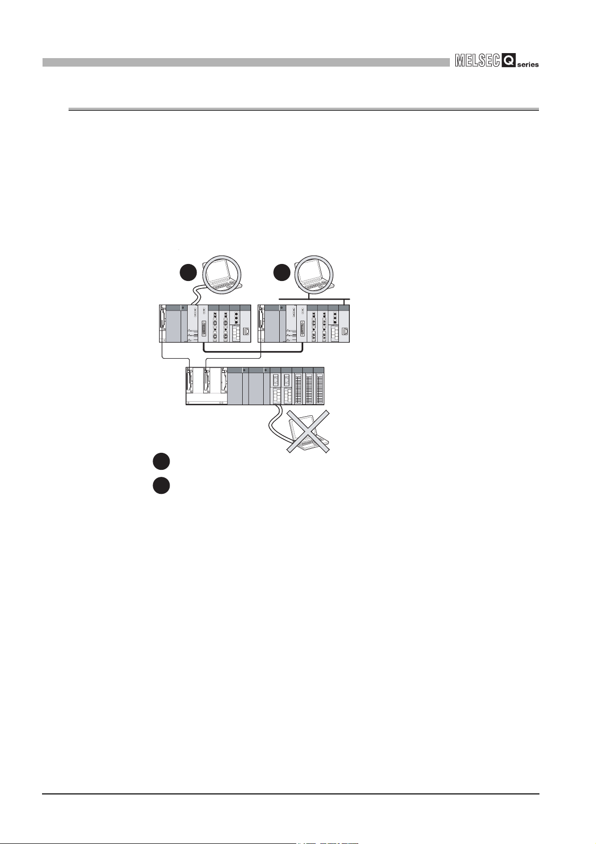
(1) When using the A/D converter module with Redundant CPU
(a) Dedicated instruction
The dedicated instruction cannnot be used.
(b) GX Configurator-AD connection
GX Configurator-AD cannot be used when accessing Redundant CPU via an
intelligent function module on an extension base unit from GX Developer.
Connect a personal computer with a communication path indicated below.
2 - 3
2.2 Precautions on System Configuration
2
-C
Function version
Relevant regulation
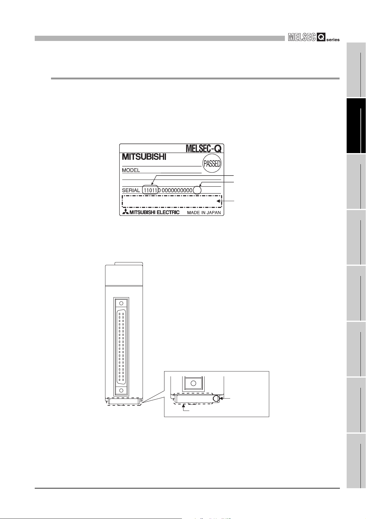
standards
Serial No. (Upper 5 digits)
SYSTEM CONFIGURATION
2.3 How to Check the Function Version, Serial No., and Software
Version
1
(1) Checking the function version and serial No.
The serial No. and function version of the A/D converter module can be checked on
the rating plate, front of the module, and system monitor of GX developer.
(a) On the rating plate
The rating plate is put on the side of the A/D converter module.
(b) On the front of the module
The function version and serial No. on the rating plate is also indicated on the
front of the module (lower part)
2
SYSTEM
3
4
SETUP AND
PROCEDURES
5
OVERVIEW
CONFIGURATION
SPECIFICATIONS
BEFORE OPERATION
1101120000000000-C
Serial No.
2.3 How to Check the Function Version, Serial No., and Software Version
Function version
UTILITY PACKAGE
(GX CONFIGURATOR-
AD)
6
PROGRAMMING
7
ONLINE MODULE
CHANGE
8
TROUBLESHOOTING
2 - 4
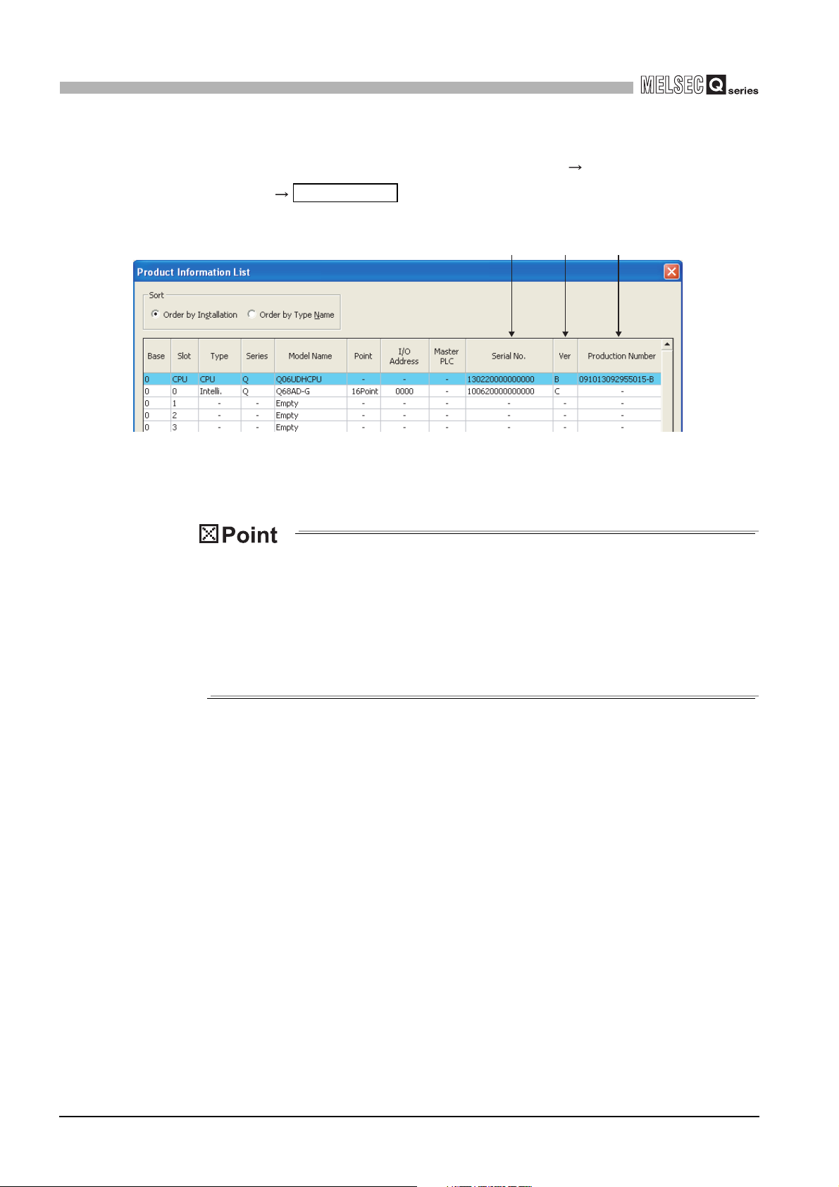
2
Product Inf. List
Serial
No.
Function
version
Product
No.
SYSTEM CONFIGURATION
(c) On the system monitor (product information list)
To display the system monitor, select [Diagnostics] [System moni-
tor] of GX Developer.
1) Production number
Production number indication is not available for the A/D converter module; "-"
is shown.
The serial No. on the rating plate and the front of the module may be different from
the serial No. displayed on the product information list in GX Developer.
• The serial No. on the rating plate and the front of the module indicates the
management information of the product.
• The serial No. displayed on the product information list in GX Developer
indicates the function information of the product. The function information
of the product is updated when a new function is added.
2 - 5
2.3 How to Check the Function Version, Serial No., and Software Version
2
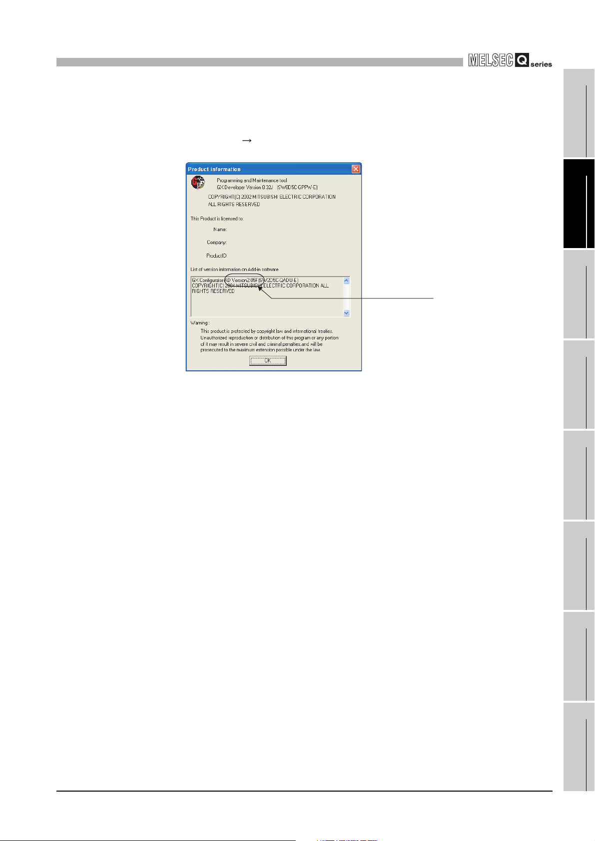
(In the case of GX Developer Version 8)
Software version
SYSTEM CONFIGURATION
(2) Checking the software version of GX Configurator-AD
The software version of GX Configurator-AD can be checked on GX Developer by
clicking [Help] [Product information].
1
2
SYSTEM
3
4
OVERVIEW
CONFIGURATION
SPECIFICATIONS
SETUP AND
PROCEDURES
BEFORE OPERATION
5
UTILITY PACKAGE
(GX CONFIGURATOR-
AD)
6
PROGRAMMING
7
ONLINE MODULE
CHANGE
8
2.3 How to Check the Function Version, Serial No., and Software Version
TROUBLESHOOTING
2 - 6
3
SPECIFICATIONS
3 SPECIFICATIONS
The description of this chapter and later is based on the Q68AD-G.
3.1 Performance Specifications
3.1.1 Performance specifications list
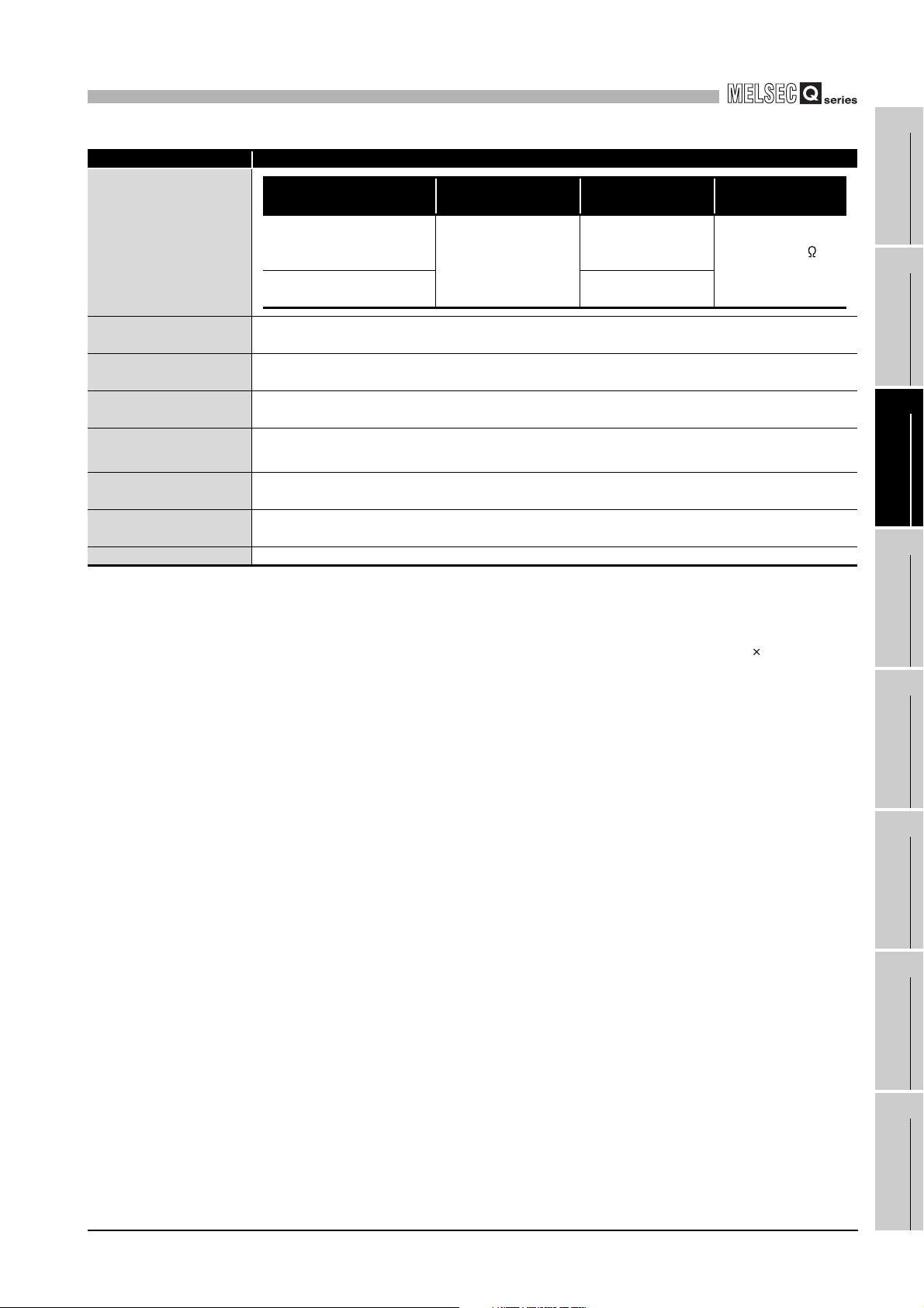
Table 3.1 shows the performance specifications of the A/D converter modules.
Table3.1 Performance Specifications of Q68AD-G
Item Specifications
Number of analog input
channels
Analog input
Digital output
Using scaling function 16-bit signed binary (-32768 to 32767)
Voltage
Current
16-bit signed binary (normal resolution mode: –4096 to 4095, high resolution mode: –12288 to 12287,
-10 to 10VDC (Input impedance 1 M or more)
0 to 20mADC (Input resistance 250 )
8 channels
–16384 to 16383)
I/O characteristics,
maximum resolution
Accuracy
(Accuracy
relative to
digital output
value)
Common mode
characteristic
Sampling cycle
Response time
Absolute maximum input
*7
Reference
accuracy
Temperature
coefficient
*4
*5
Normal resolution mode High resolution mode
Input Analog input range
0 to 10V
0 to 5V 1.25 mV
1 to 5V 1.0 mV 0.333 mV
1 to 5V
Voltage
Current
*1
*3
(Extended mode)
-10 to 10V
Users range setting
0 to 20mA
4 to 20mA
4 to 20mA
(Extended mode)
Users range setting -4000 to 4000
Normal resolution mode : ±4digit
High resolution mode (0 to 10V, -10 to 10V) : ±16digit
High resolution mode (Other than the above ranges) : ±12digit
Common mode voltage, Input-Common ground (input voltage 0V): 500VAC
Common mode voltage rejection ratio (VCM < 500V): 60Hz 107dB, 50Hz 106dB
Voltage: ± 15V Current: ± 30mA
Digital
output value
0 to 4000
-1000 to 4500 1.0 mV
-4000 to 4000
0 to 4000
-1000 to 4500
±0.1%
±71.4ppm/°C (0.00714%/°C)
10ms/ channel
20ms
Maximum
resolution
2.5 mV 0 to 16000 0.625 mV
2.5 mV
0.375 m V
5A
4 A 1.33 A
4A
1.37 A
*8
*8
*2
*6
Digital
output value
0 to 12000
-3000 to
13500
-16000 to
16000
-12000 to
12000
0 to 12000
-3000 to
13500
-12000 to
12000
*2
*2
Maximum
resolution
0.416 mV
0.333 mV
0.625 mV
0.333 mV
1.66 A
1.33 A
1.33 A
*8
*8
3 - 1
3.1 Performance Specifications
3.1.1 Performance specifications list
3
SPECIFICATIONS
1
Table3.1 Performance Specifications of Q68AD-G
Item Specifications
Specific isolated area Isolation method
Between input terminal and
Isolation
Maximum number of writes
to flash memory
Number of I/O occupied
points
External wiring connection
system
Applicable wire size
External device connection
connector
Internal current
consumption (5VDC)
Weight 0.16kg
programmable controller
power supply Transformer isolation
Between analog input
channels
Up to 50,000 times
16 points (I/O assignment: Intelligent 16 points)
40-pin connector
2
0.3mm
(AWG22) or less (for A6CON1, A6CON4)
0.088mm
*1 Accuracy of offset/gain setting at ambient temperature
*2 "digit" indicates a digital value.
*3 Accuracy per temperature change of 1°C
Example) Accuracy when temperature changes from 25 to 30°C
0.1% (reference accuracy) + 0.00714 %/°C (temperature coefficient) 5°C
(temperature change difference) = 0.1357%
*4 The cycle in which A/D conversion values are updated.
*5 The time required for an input signal to reach the A/D converter inside the Q68AD-G.
*6 Current value indicates value of instant input current that does not break module inner electrical
resistance.
*7 For details on I/O conversion characteristics, refer to Section3.1.2 (1).
*8 The maximum resolution for the user range setting
2
to 0.24mm2(AWG28 to 24) (for A6CON2)
A6CON1, A6CON2, A6CON4 (sold separately)
0.46A
Dielectric withstand
voltage
500VAC rms, 1min.
1000VAC rms, 1min.
Insulation resistance
500VDC, 10M or
more
2
SYSTEM
3
4
SETUP AND
PROCEDURES
5
UTILITY PACKAGE
(GX CONFIGURATOR-
6
OVERVIEW
CONFIGURATION
SPECIFICATIONS
BEFORE OPERATION
AD)
3.1 Performance Specifications
3.1.1 Performance specifications list
3 - 2
PROGRAMMING
7
ONLINE MODULE
CHANGE
8
TROUBLESHOOTING
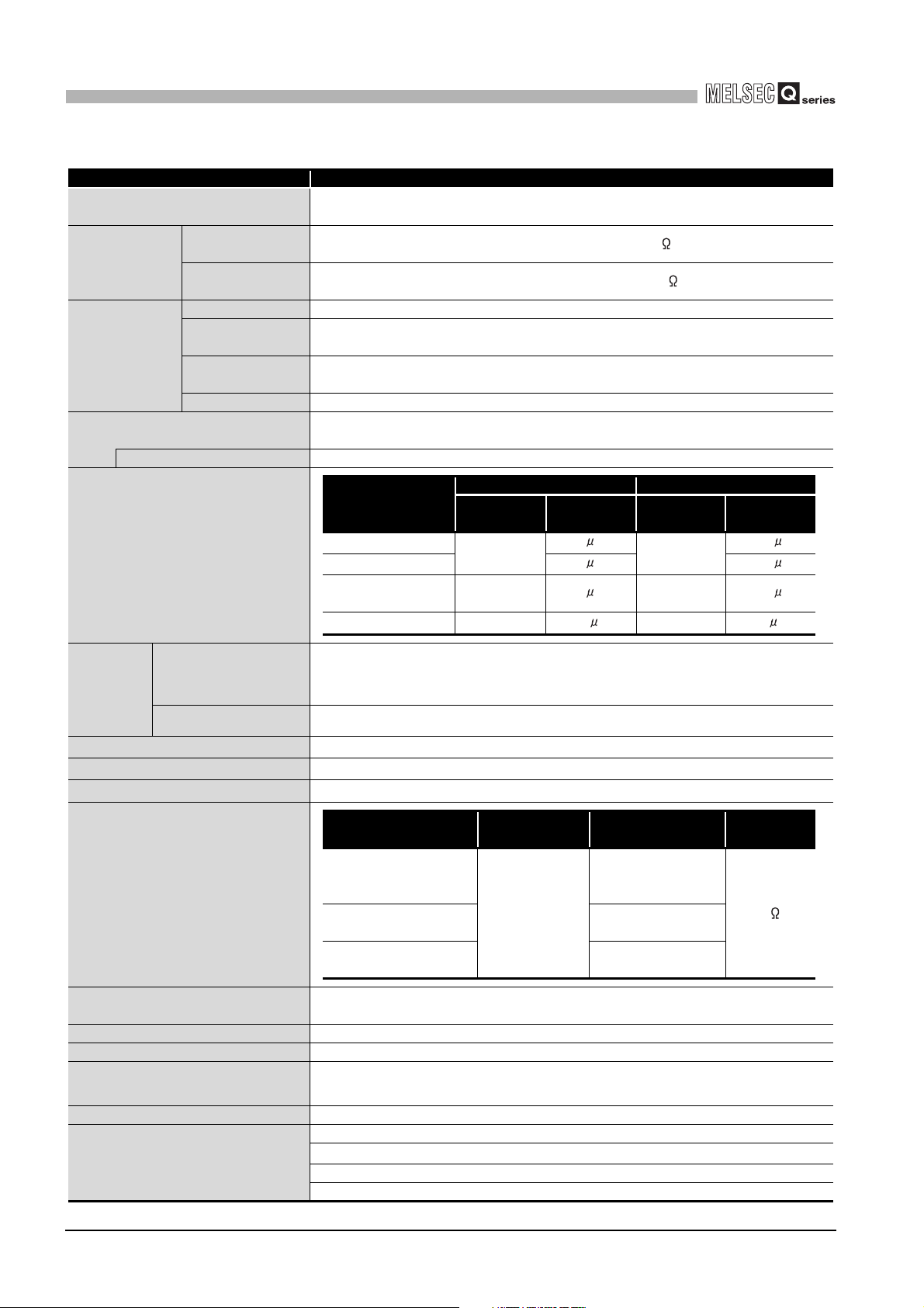
3
Number of analog input channels (2-wire
transmitters)
Input
specification
Power supply part
for 2-wire transmitter
Digital output
I/O characteristics, maximum resolution
SPECIFICATIONS
Item Specifications
With 2-wire
transmitter
Without 2-wire
transmitter
Supply voltage 26±2VDC
Maximum supply
current
Short-circuit
protection
Check terminals Available
Using scaling function 16-bit signed binary (-32768 to 32767)
Table3.2 Performance Specifications of Q66AD-DG
6 channels
4 to 20mADC (Input resistance 250 )
0 to 20mADC±1 (Input resistance 250 )
24mADC
Available
Limit current: 25 to 35mA
16-bit signed binary (normal resolution mode: –96 to 4095, high resolution mode:
–288 to 12287)
Normal resolution mode High resolution mode
Analog input range
*8
(Extended mode)
Users range setting
0 to 20mA
4 to 20mA
4 to 20mA
Digital out-
put value
0 to 4000
-1000 to 4500
*4
0 to 4000
Maximum
resolution
1.37 A
Digital out-
put value
5A
4 A 1.33 A
4A
*9
0 to 12000
-3000 to
13500
0 to 12000
Maximum
resolution
1.66 A
1.33 A
1.33 A
*9
Accuracy
(Accuracy
relative to
digital
output value)
Sampling cycle
Response time
Absolute maximum output
Isolation
Maximum number of writes to flash
memory
Number of I/O occupied points 16 points (I/O assignment: Intelligent 16 points)
External wiring connection system 40-pin connector
Applicable wire size
External device connection connector A6CON1, A6CON2, A6CON4 (sold separately)
External power supply
Reference accuracy
Temperature coefficient
*5
*6
*10
*1
*3
Specific isolated area Isolation method
Between I/O terminal and
programmable controller
power supply
Between analog input
channels
Between external power
supply and analog input
0.088mm
(Normal resolution mode: ±4digit
High resolution mode: ±12digit *2)
±71.4ppm/°C (0.00714 %/°C)
Transformer
2
0.3mm
(AWG22) or less (for A6CON1, A6CON4)
2
to 0.24mm2(AWG28 to 24) (for A6CON2)
Ripple, spike within 500mV
Inrush current : 5.0A, within 400µs
±0.1%
10ms/ channel
20ms
*7
±30mA
Dielectric withstand
500VAC rms, 1min.
isolation
Up to 50,000 times
24VDC +20%, -15%
1000VAC rms, 1min.
500VAC rms, 1min.
0.36A
*2
voltage
P-P
Insulation
resistance
500VDC
10M or
more
3 - 3
3.1 Performance Specifications
3.1.1 Performance specifications list
3
Remark
Internal current consumption (5VDC) 0.42A
Weight 0.22kg
SPECIFICATIONS
Table3.2 Performance Specifications of Q66AD-DG
Item Specifications
*1 Accuracy of offset/gain setting at ambient temperature
Q66AD-DG needs to be powered on 30 minutes prior to operation for compliance to the
specification (accuracy).
*2 "digit" indicates a digital value.
*3 Accuracy per temperature change of 1°C
Example) Accuracy when temperature changes from 25 to 30°C
0.1% (reference accuracy) + 0.00714 %/°C (temperature coefficient) 5°C
(temperature change difference) = 0.1357%
*4 User range setting is 2 to 24mA
*5 The cycle in which A/D conversion values are updated.
*6 The time required for an input signal to reach the A/D converter inside the Q66AD-DG.
*7 Current value indicates value of instant input current that does not break module inner electrical
resistance.
*8 For details on I/O conversion characteristics, refer to Section3.1.2 (2).
*9 The maximum resolution for the user range setting
*10 The external power supply is for a 2-wire transmitter.
When all the channels used are for current input, wiring for 24VDC is not required.
Note that to use the Q66AD-DG with a product number (first five digits) of 15031 or earlier, refer to
Appendix 2.
1
2
SYSTEM
3
4
OVERVIEW
CONFIGURATION
SPECIFICATIONS
See the user's manual for the CPU module being used for general specifications
of the A/D converter modules.
SETUP AND
PROCEDURES
BEFORE OPERATION
5
UTILITY PACKAGE
(GX CONFIGURATOR-
AD)
6
PROGRAMMING
7
ONLINE MODULE
CHANGE
8
3.1 Performance Specifications
3.1.1 Performance specifications list
TROUBLESHOOTING
3 - 4

3
SPECIFICATIONS
3.1.2 I/O conversion characteristic
The I/O conversion characteristic represents the angle formed by a straight line
connecting the "offset value" and "gain value" when the analog signals (voltage or current
input) from outside the programmable controller are converted to digital values.
Offset value
The offset value denotes the analog input value (voltage or current) that makes the digital
output value 0.
Gain value
The gain value denotes the analog input value (voltage or current) that makes the digital
output value:
4000 (in normal resolution mode)
16000/12000 (in high resolution mode)
3 - 5
3.1 Performance Specifications
3.1.2 I/O conversion characteristic

3
1) 1 to 5V
12287
12000
4095
4000
0
-96
-288
0
Analog input practical range
High resolution mode
Normal resolution
mode
Digital output value
Analog input voltage (V)
01 5
Analog input practical range
Digital output value
Analog input voltage (V)
3) -10 to 10V
16383
16000
4095
4000
-4000
-4096
-16000
-16384
0
0
0
10-10
High resolution mode
Normal resolution mode
Analog input practical range
Digital output value
Analog input voltage (V)
4) 0 to 10V
0
0
10
16383
16000
4095
4000
0
-96
-384
Normal resolution mode
High resolution mode
SPECIFICATIONS
(1) Input characteristics of Q68AD-G
(a) Voltage input characteristic
Fig. 3.1 shows a graph of the voltage input characteristic.
2) 0 to 5V
Analog input practical range
1
OVERVIEW
2
12287
12000
4095
4000
0
-96
-288
Digital output value
High resolution mode
0
05
Analog input voltage (V)
Normal resolution
mode
SYSTEM
3
4
SETUP AND
PROCEDURES
5
CONFIGURATION
SPECIFICATIONS
BEFORE OPERATION
Fig.3.1 Voltage input characteristic of Q68AD-G (1/2)
3.1 Performance Specifications
3.1.2 I/O conversion characteristic
3 - 6
UTILITY PACKAGE
(GX CONFIGURATOR-
AD)
6
PROGRAMMING
7
ONLINE MODULE
CHANGE
8
TROUBLESHOOTING

Analog input practical range
Digital output value
Analog input voltage (V)
3) -10 to 10V
16383
16000
4095
4000
-4000
-4096
-16000
-16384
0
0
0
10-10
High resolution mode
Normal resolution mode
3
SPECIFICATIONS
Fig.3.1 Voltage input characteristic of Q68AD-G (2/2)
(1) Set within the analog input range and digital output range for each input
range. If these ranges are exceeded, the maximum resolution and accuracy
may not fall within the performance specifications. (Avoid use shown by the
dotted lines in Fig.3.1.)
(2) Do not input an analog input voltage of -15V or less and 15V or more The
input elements may be damaged.
(3) Set the offset/gain values for the User range setting marked within a range
which satisfies the following conditions.
(a) Offset value, gain value setting range: 10 to 10V
(b) Use one of the following formulas according to the resolution mode to be
set.
1) Normal resolution mode
{ (Gain value) - (Offset value) } > 1.5V
2) High resolution mode
{ (Gain value) - (Offset value) } 4.0V
(4) When an analog value that exceeds the range for the digital output value is
entered, the digital output value will be fixed at the maximum or minimum
value.
Analog input
range setting
1 to 5V
0 to 5V
-10 to 10V -4096 -16384
0 to 10V -96 -384
1 to 5V
(Extended mode)
User range setting -4096 4095 -12288 12287
Normal resolution mode High resolution mode
Minimum Maximum Minimum Maximum
-96
4095
-1096 4595 -3288 13787
-288 12287
16383
3 - 7
3.1 Performance Specifications
3.1.2 I/O conversion characteristic

3
0
04
0
20
12287
4000
12000
4095
-288
-96
Practical analog input range
Digital output value
Normal resolution
mode
High resolution
mode
1) 4 to 20mA
Analog input current (mA)
20 22
Analog input practical range
Digital output value
Analog input current (mA)
3) 4 to 20mA (Expanded mode)
004
0
-1000
-1096
-3000
-3288
High resolution
mode
Normal resolution
mode
13787
13500
12000
4595
4500
4000
SPECIFICATIONS
1
(b) Current input characteristic
Fig. 3.2 shows a graph of the current input characteristic
2) 0 to 20mA
12287
12000
4095
4000
0
-96
-288
Digital output value
Analog input practical range
High resolution mode
Normal resolution
mode
0
0
Analog input current (mA)
OVERVIEW
2
SYSTEM
CONFIGURATION
3
20
SPECIFICATIONS
4
SETUP AND
PROCEDURES
BEFORE OPERATION
5
Fig.3.2 Current input characteristic of Q68AD-G
3.1 Performance Specifications
3.1.2 I/O conversion characteristic
3 - 8
UTILITY PACKAGE
(GX CONFIGURATOR-
AD)
6
PROGRAMMING
7
ONLINE MODULE
CHANGE
8
TROUBLESHOOTING

3
SPECIFICATIONS
(1) Set within the analog input range and digital output range for each input
range.
If these ranges are exceeded, the maximum resolution and accuracy may not
fall within the performance specifications. (Avoid use shown by the dotted
lines in Fig.3.2.)
(2) Do not input an analog input current of -30mA or less and 30mA or more.
The input elements may be damaged.
(3) Set the offset/gain values for the User range setting marked within a range in
which satisfies the following conditions.
(a) Gain value 20mA, offset value 0mA
(b) Use one of the following formulas according to the resolution mode to be
(4) When an analog value that exceeds the range of the digital output value is
entered, the digital output value will be fixed at the maximum or minimum
value.
range setting
(Extended mode)
User range setting -4096 4095 -12288 12287
set.
1) Normal resolution mode
{ (Gain value) - (Offset value) } > 5.5mA
2) High resolution mode
{ (Gain value) - (Offset value) } 16.0mA
Analog input
4 to 20mA
0 to 20mA
4 to 20mA
Digital output value
(Normal resolution mode)
Minimum Maximum Minimum Maximum
-96 4095 -288 12287
-1096 4595 -3288 13787
Digital output value
(High resolution mode)
3 - 9
3.1 Performance Specifications
3.1.2 I/O conversion characteristic

3
20 22
Analog input practical range
Digital output value
Analog input current (mA)
3) 4 to 20mA (Expanded mode)
004
0
-1000
-1096
-3000
-3288
High resolution
mode
Normal resolution
mode
13787
13500
12000
4595
4500
4000
SPECIFICATIONS
1
(2) Input characteristic of Q66AD-DG
Fig. 3.3 shows a graph of the Q66AD-DG input characteristic.
1) 4 to 20mA
12287
12000
4095
4000
0
-96
-288
Digital output value
Practical analog input range
0
04
Analog input current (mA)
High resolution
mode
Normal resolution
mode
20
2) 0 to 20mA
12287
12000
4095
4000
0
-96
-288
Digital output value
Analog input practical range
High resolution mode
0
0
Analog input current (mA)
Normal resolution
mode
20
2
SYSTEM
3
4
SETUP AND
PROCEDURES
5
OVERVIEW
CONFIGURATION
SPECIFICATIONS
BEFORE OPERATION
Fig.3.3 Input characteristic of Q66AD-DG
3.1 Performance Specifications
3.1.2 I/O conversion characteristic
3 - 10
UTILITY PACKAGE
(GX CONFIGURATOR-
AD)
6
PROGRAMMING
7
ONLINE MODULE
CHANGE
8
TROUBLESHOOTING

3
SPECIFICATIONS
(1) Set within the analog input range and digital output range for each input
range.
If these ranges are exceeded, the maximum resolution and accuracy may not
fall within the performance specifications. (Avoid use shown by the dotted
lines in Fig.3.3.)
(2) Do not input an analog input current of -30mA or less and 30mA or more.
The input elements may be damaged.
(3) Set the offset/gain values for the User range setting marked within a range
which satisfies the following conditions.
(a) Gain value 24mA, offset value 0mA
(b) Use one of the following formulas according to the resolution mode to be
(4) When an analog value that exceeds the range of the digital output value is
entered, the digital output value will be fixed at the maximum or minimum
value.
range setting
(Extended mode)
User range setting -96 4095 -288 12287
set.
1) Normal resolution mode
{ (Gain value) - (Offset value) } > 5.5mA
2) High resolution mode
{ (Gain value) - (Offset value) } 16.0mA
Analog input
0 to 20mA
4 to 20mA
4 to 20mA
Digital output value
(Normal resolution mode)
Minimum Maximum Minimum Maximum
-96 4095 -288 12287
-1096 4595 -3288 13787
Digital output value
(High resolution mode)
3 - 11
3.1 Performance Specifications
3.1.2 I/O conversion characteristic

3
SPECIFICATIONS
3.1.3 Accuracy
The reference accuracy is the accuracy at the ambient temperature for offset/gain setting.
The temperature coefficient is the accuracy per temperature variation of 1°C.
The reference accuracy is the accuracy relative to the maximum digital output value.
Even if you change the offset/gain setting or input range to change the input characteristic,
the reference accuracy and temperature coefficient do not change and are kept within the
ranges given in the performance specifications.
[Example] Accuracy when the temperature changed from 25°C to 30°C
0.1% (reference accuracy) + 0.00714%/°C (temperature coefficient) 5°C (temperature
variation difference) = 0.1357%
1
2
SYSTEM
3
4
OVERVIEW
CONFIGURATION
SPECIFICATIONS
SETUP AND
PROCEDURES
BEFORE OPERATION
5
UTILITY PACKAGE
(GX CONFIGURATOR-
AD)
6
PROGRAMMING
7
ONLINE MODULE
CHANGE
8
3.1 Performance Specifications
3.1.3 Accuracy
TROUBLESHOOTING
3 - 12

3
SPECIFICATIONS
3.2 Function List
Table 3.3 lists the functions of the A/D converter modules.
Item Function Reference section
A/D conversion enable/
disable setting
A/D conversion method
Maximum and minimum
values hold function
Input signal error
detection function
Warning output function
Conversion starting time
setting function
(Q66AD-DG only)
Supply power ON/OFF
function
(Q66AD-DG only)
Scaling function
Online module change
(1) Specifies whether to enable or disable the A/D conversion for each channel.
(2) Since the conversion time is 10ms per channel, disabling A/D conversion of
(1) Sampling processing
(2) Averaging processing
(3) Primary delay filter
(1) The maximum and minimum values of the digital output values are retained in the
(1) A voltage or current input that is equal to or more than the input signal error
(1) Process alarm
(2) Rate alarm
(1) Setting the A/D conversion starting time allows A/D conversion to be started at
(1) The supply power to the 2-wire transmitter can be switched ON/OFF channel by
(2) Power is supplied to channels that have input range settings of "4 to 20mA
(1) Conversion of A/D conversion values to preset percentage values and loading
(1) The module can be changed without the system being stopped.
Table3.3 Function list
unused channels can reduce the entire conversion time.
The A/D conversion for analog input values is performed successively for each
channel, and the digital output value is output upon each conversion.
(a) Time averaging
A/D conversion is averaged in terms of time on a channel basis and a digital
average value is output.
(b) Count averaging
A/D conversion is averaged in terms of count on a channel basis and a
digital average value is output.
(c) Move averaging
The specified number of digital output values measured per sampling time
are averaged.
A digital output value is smoothed according to the preset time constant.
module.
detection upper limit value, or equal to or less than the input signal error detection lower limit value is detected.
A warning is output when a digital output value is equal to or more than the process alarm upper upper limit value, or equal to or less than the process alarm
lower lower limit value.
A warning is output when the digital output value changes in a rate by which the
digital output value reaches the rate alarm upper limit value or more, or the rate
alarm lower limit value or less.
the point when the output of the 2-wire transmitter stabilizes.
channel.
(2-wire transmitter input): 0
H" or "User range setting (2-wire transmitter input): FH", and that are set
input): A
to "Enabled" in A/D conversion enable/disable setting (Un\G0).
into the buffer memory is available.
Programming steps for the scaling can be eliminated.
H", "4 to 20mA (Extended mode) (2-wire transmitter
*1
Section 3.4.2
Section 3.2.1
Section 3.2.2
Section 3.2.3
Section 3.2.4
Section 3.2.5
Section 3.4.2
Section 3.2.6
Chapter 7
3 - 13
3.2 Function List

3
SPECIFICATIONS
*1 If the module is changed online to a module that has no extended mode for analog input range under
the following input range settings, an intelligent function module switch error will occur.
Q68AD-G: 4 to 20mA (extended mode): A
1 to 5V (extended mode): B
Q66AD-DG: 4 to 20mA (extended mode) (2-wire transmitter input): A
4 to 20mA (extended mode) (current input): C
1
H
H
H
H
OVERVIEW
2
SYSTEM
CONFIGURATION
3
SPECIFICATIONS
4
SETUP AND
PROCEDURES
BEFORE OPERATION
5
UTILITY PACKAGE
(GX CONFIGURATOR-
AD)
6
PROGRAMMING
7
ONLINE MODULE
CHANGE
8
3.2 Function List
TROUBLESHOOTING
3 - 14

3
SPECIFICATIONS
3.2.1 A/D conversion methods
(1) Sampling processing
A/D conversion is performed successively for analog input values, and the
converted digital output values are stored in the buffer memory.
The sampling processing time varies depending on the number of channels used
(number of channels set as A/D conversion enable).
Sampling processing time = No. of channels used 10 (ms)
Example) When setting 6 for the number of channels used
6 10 = 60 (ms)
(2) Averaging processing
(a) Time averaging
A/D conversion is made for the preset period of time, the sum of values other than
the maximum and minimum values is averaged, and the result is stored into the
buffer memory.
The processing count within the set time varies depending on the number of
channels used (number of channels set as A/D conversion enable).
Processing count = Set time/(No. of channels used 10) (times)
Example) When setting 6 for the number of channels used, and 500ms for the
set time
500/(6 10) = 8.333 (times) Drop the fractional part.
(b) Count averaging
A/D conversion is made the preset number of times, the sum of values other than
the maximum and minimum values is averaged, and the result is stored into the
buffer memory.
The time required for the count-based average value to be stored into the buffer
memory varies depending on the number of channels used (number of channels
set as A/D conversion enable).
Processing time = Set count (No. of channels used 10) (ms)
Example) When setting 5 (times) for the average processing count
5 6 10 = 50 (ms)
(c) Moving average
The specified count of digital output values imported per sampling time are averaged to find a value, which is then stored into the buffer memory.
Since average processing is performed with data shifted per sampling, the most
recent digital output value is obtainable.
3 - 15
3.2 Function List
3.2.1 A/D conversion methods

3
Yn = Yn-1 +
t
t + TA
(yn - Yn-1)
SPECIFICATIONS
Moving average processing at the preset count of 4 times
A/D conversion
value
12000
1
Sampling time
3) 4)
2)
1)
5)
6)
8) 9)
7)
10) 11)
12)
OVERVIEW
2
6000
0
Data transition inside buffer memory
First storage
1)+2)+3)+4) 2)+3)+4)+5) 3)+4)+5)+6)
A/D conversion completed flag ON
Second storage
4
4
First storage
Second storage
Third storage
Time [ms]
Third storage
4
Buffer memory
Digital output value
(3) Primary delay filter
A digital value whose transient noise has been smoothed is output according to the
preset time constant.
The degree of smoothing varies with the time constant setting.
The relational expression of the time constant and digital output value is indicated
below.
[If n = 1*1]
Yn = 0
SYSTEM
3
4
SETUP AND
PROCEDURES
5
CONFIGURATION
SPECIFICATIONS
BEFORE OPERATION
[If n = 2]
t
Yn = yn-1 +
t + TA
(yn - yn-1)
[If n 3]
Yn : Current digital output value yn : Pre-smoothing digital output value
Yn-1 : Immediately preceding digital output
value
n : Sampling count
TA : Time constant (s)
*1 The A/D conversion completed flag turns ON when n 2.
Yn-1 : Immediately preceding
pre-smoothing digital output value
:
t
3.2.1 A/D conversion methods
A/D conversion time (0.01
number of conversion enabled channels)(s)
3.2 Function List
3 - 16
UTILITY PACKAGE
(GX CONFIGURATOR-
AD)
6
PROGRAMMING
7
ONLINE MODULE
CHANGE
8
TROUBLESHOOTING

3
Analog input value Digital output value
0 1000
0
0.2
0.4
0.6
0.8
1
1.2 12000
10000
0
2000
4000
6000
8000
Elapsed time (ms)
Analog input value (V)
Digital output value
Digital output value
(moving average processing: 16 times)
Digital output value
(time constant setting: 2000ms)
0
0
0.2
0.4
0.6
0.8
1
1.2 12000
10000
0
2000
4000
6000
8000
Analog input value
Digital output value
(time constant setting: 1000ms)
Elapsed time (ms)
Analog input value (V)
Digital output value
SPECIFICATIONS
[Example 1] Digital output value when the analog input value varied from 0 to 1V
When the high resolution mode and the input range of 0 to 10V is
specified for the Q68AD-G
The variation of the digital output value at the time constant setting of
1000ms (1s) is as shown below.
1000ms (1s) after the analog input value has reached 1V, the digital
output value reaches 63.2% of the value attained when the sampling
processing is selected.
[Example 2] Digital output value when the variation of the analog input value has a
ringing waveform
When the high resolution mode and the input range of 0 to 10V is
specified for the Q68AD-G
The variations of the digital output values at the time constant setting
of 2000ms (2s), at the time constant setting of 1000ms (1s), and at
the moving average processing of 16 times are as shown below.
3 - 17
3.2 Function List
3.2.1 A/D conversion methods

3
SPECIFICATIONS
3.2.2 Maximum and minimum values hold function
(1) The maximum and minimum values are held in the buffer memory channel by
channel.
(2) The maximum and minimum values are cleared to 0 when the maximum value/
minimum value reset request (YD) or operating condition setting request (Y9) is
turned ON, and new maximum and minimum values are stored when conversion is
started.
(3) Since the area for storing the maximum and minimum values can be rewritten with the
sequence program, the maximum and minimum values within a specific period of time
can be checked.
(4) When the scaling function is enabled, values after scaling conversion are stored as
the maximum and minimum values.
For the scaling function, refer to Section 3.2.6.
1
2
SYSTEM
3
OVERVIEW
CONFIGURATION
3.2.3 Input signal error detection function
(1) If the input voltage/current rose to or above the input signal error detection upper limit
value or fell to or below the lower limit value, the input signal error detection flag
(Un\G49) and input signal error detection signal (XC) turn ON and the ALM LED
flickers to indicate the error.
(2) When the input signal error detection flag (Un\G49) turns ON for a channel, a digital
output value immediately before the error detection is held for the channel, and the
A/D conversion completed flag (Un\G10) of the corresponding channel turns OFF.
(3) By bringing the analog input value within the setting range and then turning ON the
error clear request (YF), the input signal error detection flag (Un\G49) and input signal
error detection signal (XC) turn OFF.
SPECIFICATIONS
4
SETUP AND
PROCEDURES
BEFORE OPERATION
5
UTILITY PACKAGE
(GX CONFIGURATOR-
AD)
6
PROGRAMMING
7
3.2 Function List
3.2.2 Maximum and minimum values hold function
3 - 18
ONLINE MODULE
CHANGE
8
TROUBLESHOOTING

3
SPECIFICATIONS
(4) When the analog input value returns to within the setting range, A/D conversion is
resumed independently of whether the input signal error detection flag (Un\G49) and
input signal error detection signal (XC) are reset or not, the A/D conversion completed
flag (Un\G10) of the corresponding channel turns ON again after the first updating.
(The ERR. LED remains flickering.)
Analog input value
Upper limit
value
CH1 analog
input value
Lower limit
value
Error detection
Input value
normal
Time
CH1 input signal error detection flag
Input signal error detection signal
CH1 A/D conversion completed flag
Error clear request (YF)
(5) This function is executed at every sampling processing.
(6) Perform the following procedure to use this function.
1) Set the input signal error detection setting value for the corresponding channel.
2) Enable the A/D conversion of the corresponding channel.
3) Enable the input signal error detection of the corresponding channel.
4) Turn ON the operating condition setting request (Y9).
(Un\G49.b0)
(XC)
(Un\G10.b0)
3 - 19
3.2 Function List
3.2.3 Input signal error detection function

3
=
Input signal error detection
setting value
(Input signal error detection
upper limit setting value)
Gain value of each range-
Input signal error detection
upper limit value
Gain value of each range - Offset value of each range
1000
=
Input signal error detection
setting value
(Input signal error detection
lower limit setting value)
Input signal error detection
lower limit value
-
Lower limit value of each
range
Gain value of each range - Offset value of each range
1000
SPECIFICATIONS
(7) How to set an input signal error detection upper/lower limit values
Set input signal error detection upper/lower limit values based on the input signal error
detection setting value (input signal error detection upper/lower limit setting values).
(Set the values in the unit of 1 (0.1%)).
The input signal error detection setting value is reflected to both the input signal error
detection upper and lower limit values by default.
To detect input signal errors using only an upper limit value or lower limit value, or to
individually set an upper limit value and a lower limit value, refer to (9) in this section.
(a) Input signal error detection upper limit value
This value is calculated as follows:
Gain value + {Full input range (Gain value - Offset value)
detection setting value (Input signal error detection upper limit setting value)}
A value equal to or greater than the gain value can be set.
A setting value (%) can be calculated by the following formula.
(b) Input signal error detection lower limit value
This value is calculated as follows:
Lower limit value of the input range - {Full input range (Gain value - Offset value)
Input signal error detection setting value (Input signal error detection lower limit
setting value)}
A value equal to or smaller than the lower limit value of the input range can be set.
A setting value (%) can be calculated by the following formula.
× Input signal error
×
1
2
SYSTEM
3
4
SETUP AND
PROCEDURES
5
OVERVIEW
CONFIGURATION
SPECIFICATIONS
BEFORE OPERATION
3.2 Function List
3.2.3 Input signal error detection function
3 - 20
UTILITY PACKAGE
(GX CONFIGURATOR-
AD)
6
PROGRAMMING
7
ONLINE MODULE
CHANGE
8
TROUBLESHOOTING

3
Remark
SPECIFICATIONS
The following table lists the lower limit value, offset value, and gain value for each
input range
Table3.4 The lower limit value, offset value, and gain value for each input range (Q68AD-G)
Input Analog input range Lower limit value Offset value Gain value
0 to 10V 0V 10V
0 to 5V 0V 5V
1 to 5V 1V 5V
Volt-
age
Cur-
rent
1 to 5V (extended mode) 1V 5V
-10 to 10V -10V 0V 10V
Analog value when the digital value is:
User range setting
0 to 20mA 0mA 0mA 20mA
4 to 20mA 4mA 4mA 20mA
4 to 20mA (extended mode) 4mA 4mA 20mA
User range setting
• -4000 (normal resolution mode)
• -12000 (high resolution mode)
Analog value when the digital value is:
• -4000 (normal resolution mode)
• -12000 (high resolution mode)
Analog value set as an
offset value by the user
Analog value set as an
offset value by the user
Analog value set as a
gain value by the user
Analog value set as a
gain value by the user
Table3.5 The lower limit value, offset value, and gain value for each input range (Q66AD-DG)
Input Analog input range Lower limit value Offset value
0 to 20mA 0mA 20mA
4 to 20mA 4mA 20mA
4 to 20mA (extended mode) 4mA 20mA
User range setting Analog value set as an offset value by the user
Analog value set as a
gain value by the user
3 - 21
3.2 Function List
3.2.3 Input signal error detection function

3
=
Input signal error detection
setting value
Input signal error detection
upper limit value
-
Lower limit value of each
range
Gain value of each range - Offset value of each range
1000
Input signal error detection
upper limit value
21.6mA
Offset value
20mA
Gain value
4mA
Input signal error detection
lower limit value
Error
Error
1.6mA
(10.0 of 1.6mA)
1.6mA
(10.0 of 1.6mA)
16mA
(Gain value - Offset value)
2.4mA
SPECIFICATIONS
(8)Setting example of input signal error detection
Example) To detect an input signal error when the analog input value falls below
Apply the following values to the calculation formula for an input signal error detection
lower limit value.
• Input signal error detection lower limit value: 2.4mA
• Lower limit value of the input range (offset value): 4.0mA
• Gain value: 20.0mA
Therefore, Set 100 (10.0%) as an input signal error detection setting value.
The input signal error detection values act as follows in this case. (Because of the setting value of 100 (10%), an error is detected not only at 2.4mA but also at 21.6mA.)
2.4mA in the channel where the input range of 4 to 20mA (extended
mode) and the normal resolution mode is set
1
2
SYSTEM
3
4
OVERVIEW
CONFIGURATION
SPECIFICATIONS
SETUP AND
PROCEDURES
BEFORE OPERATION
5
UTILITY PACKAGE
(GX CONFIGURATOR-
AD)
6
PROGRAMMING
7
ONLINE MODULE
CHANGE
8
3.2 Function List
3.2.3 Input signal error detection function
TROUBLESHOOTING
3 - 22

3
Input signal error detection
upper limit value
21.6mA
Offset value
20mA
Gain value
4mA
Input signal error detection
lower limit value
No error detected
Error
1.6mA
(10.0 of 16mA)
1.6mA
(10.0 of 16mA)
16mA
(Gain value - Offset value)
2.4mA
SPECIFICATIONS
(9)Specifying a condition to detect input signal errors
By setting the following buffer memory areas, input signal errors can be detected only
at an upper limit value or lower limit value, or at different upper/lower limit values.
• Input signal error detection extended/input signal error detection setting (Un\G47)
•CH input signal error detection setting value/CH input signal error detection
lower limit setting value (Un\G142 to Un\G149)
•CH input signal error detection upper limit setting value (Un\G150 to Un\G157)
The following is a setting example.
Example) Channel where the input range of 4 to 20mA (extended mode) and the
normal resolution mode is set
1) To detect input signal errors at a lower limit value only
• Input signal error detection extended setting: 1 (different upper/lower limit
values)
• Input signal error detection upper limit setting value: 251 (input signal error
detection disabled)
• Input signal error detection lower limit setting value: 100 (10.0%)
3 - 23
3.2 Function List
3.2.3 Input signal error detection function

3
Input signal error detection
upper limit value
21.6mA
Offset value
20mA
Gain value
4mA
Input signal error detection
lower limit value
Error
No error
detected
1.6mA
(10.0 of 16mA)
1.6mA
(10.0 of 16mA)
16mA
(Gain value - Offset value)
2.4mA
Input signal error detection
upper limit value
20.8mA
Offset value
20mA
Gain value
4mA
Input signal error detection
lower limit value
Error
Error
0.8mA
(5.0 of 16mA)
1.92mA
(12.0 of 16mA)
16mA
(Gain value - Offset value)
2.08mA
SPECIFICATIONS
2) To detect input signal errors at an upper limit value only
• Input signal error detection extended setting: 1 (different upper/lower limit
values)
• Input signal error detection upper limit setting value: 100 (10.0%)
• Input signal error detection lower limit setting value: 251 (input signal error
detection disabled)
1
2
SYSTEM
3
4
OVERVIEW
CONFIGURATION
SPECIFICATIONS
3) To detect input signal errors at different upper and lower limit values
• Input signal error detection extended setting: 1 (different upper/lower limit
values)
• Input signal error detection upper limit setting value: 50 (5.0%)
• Input signal error detection lower limit setting value: 120 (12.0%)
SETUP AND
PROCEDURES
BEFORE OPERATION
5
UTILITY PACKAGE
(GX CONFIGURATOR-
AD)
6
PROGRAMMING
7
ONLINE MODULE
CHANGE
8
3.2 Function List
3.2.3 Input signal error detection function
TROUBLESHOOTING
3 - 24

3
SPECIFICATIONS
3.2.4 Warning output function
(1) Process alarm
(a) If the detected digital output value rose to or above the process alarm upper upper
limit value or fell to or below the process alarm lower lower limit value and entered
the warning output range zone, the warning output flag (process alarm)(Un\G50)
and warning output signal (X8) turn ON and the ALM LED is lit to indicate the
warning.
A warning will be output according to the following digital output values.
Item Digital value causing warning output
Value set in scaling enable/
disable setting (Un\G53)
(b) After a warning was output, when the digital output value reaches a value less
than the process alarm upper lower limit value, or a value more than the process
alarm lower upper limit value, "0" is stored in the corresponding bit of the warning
output flag (Un\G50) for the channel.
The warning output signal (X8) turns OFF, and the ALM LED turns OFF when the
digital output values in all channels get out of the warning output range.
0: Disable
1: Enable
CH digital output value (Un\G11 to Un\G18)
CH scaling value (Un\G54 to Un\G61)
Digital output value
Upper upper
limit value
Upper lower
limit value
CH1 digital output
value
Lower upper
limit value
Lower lower
limit value
CH1 process alarm upper limit value
(Un\G50.b0)
CH1 process alarm lower limit value
(Un\G50.b1)
CH2 process alarm upper limit value
(Un\G50.b2)
Warning output signal (X8)
Warning
occurrence
CH2 digital
output value
Warning
occurrence
Warning cancel
Warning
occurrence
Warning output range
Warning output range outside
Included
Warning cancel
Warning cancel
Time
3 - 25
(c) When time or count averaging is specified, this function is executed at intervals of
the preset averaging time or averaging count.
When any other A/D conversion system (sampling processing, moving average,
primary delay filter) is specified, this function is executed at intervals of the
sampling time.
(d) To use the scaling function, be sure to consider scale conversion before setting
the CH process alarm upper/lower limit value.
3.2 Function List
3.2.4 Warning output function

3
Time
Rate alarm
warning detection
period
Varying rate (%) of
digital output value
Time
Rate alarm
warning detection
period
Rate alarm
upper limit
value
Varying rate of
CH1 digital
output value
Rate alarm
lower limit
value
Varying rate of
CH2 digital
output value
Digital output value
CH1 digital
output value
CH2 digital
output value
CH1 rate alarm upper limit value
(Un\G51.b0)
CH1 rate alarm lower limit value
(Un\G51.b1)
CH2 rate alarm lower limit value
(Un\G51.b2)
Warning output signal (X8)
SPECIFICATIONS
(2) Rate alarm
(a) If the range of change in the digital output value sampled at intervals of the rate
alarm warning detection period is equal to or greater than the rate alarm upper
limit value or is equal to or less than the rate alarm lower limit value, the warning
output flag (rate alarm) (Un\G51) and warning output signal (X8) turn ON and the
ALM LED is lit to indicate the warning of the rate alarm.
(b) If, after the output of the warning, the rate fell below the rate alarm upper limit
value or rose above the rate alarm lower limit value and returned to within the setting range, "0" is stored into the bit position corresponding to the channel
number of the warning output flag (rate alarm) (Un\G51).
The warning output signal (X8) turns OFF only when all channels return to within
the setting range.
1
2
SYSTEM
3
4
OVERVIEW
CONFIGURATION
SPECIFICATIONS
SETUP AND
PROCEDURES
BEFORE OPERATION
5
UTILITY PACKAGE
(GX CONFIGURATOR-
AD)
6
PROGRAMMING
7
3.2 Function List
3.2.4 Warning output function
3 - 26
ONLINE MODULE
CHANGE
8
TROUBLESHOOTING

3
Rate alarm lower limit value
Time
Rate alarm upper limit value
+30%
+20%
0
Varying rate (%) of
digital output value
SPECIFICATIONS
(c) Set the rate alarm upper limit value/lower limit value in 0.1%/s increments relative
to the maximum value (16000/12000/4000) of the digital output value.
The setting range is -32768 to 32767 (-3276.8% to 3276.7%).
(d) The setting range of the rate alarm warning detection period is 10 to 5000ms.
When the period is set to 5000ms, the digital values are compared at intervals of 5
seconds to detect the varying rate.
(e) The rate alarm is judged by converting the rate alarm upper/lower limit value into
the digit value per rate alarm warning detection period.
The expression for the value used to make judgment per rate alarm warning
detection period is as follows.
Value used to make judgment per rate alarm warning detection period [digit]
=rate alarm upper limit value or lower limit value 0.001 maximum value of the
digital output value rate alarm warning detection period 1000
Example
In channel 1, when the following:
• Upper limit value of change rate: 30%/s (300 is stored in buffer memory)
• Maximum digital output value: 16000
• Rate alarm warning detection period: 10ms
are set, a value [digit] used at every rate alarm warning detection period can be
calculated as follows:
300 0.001 16000 10 1000=48(digit)
Therefore, the current value is compared with the previous value every 10ms in
channel 1, and whether a difference of 48 (digit) or more is identified between
them or not is determined.
(f) The rate alarm is useful to watch the varying rate of the digital output value in a
limited range.
1) Example of setting the rate alarm upper limit value/lower limit value when it is
desired to watch that the digital output value increases within the specified
range
3 - 27
3.2 Function List
3.2.4 Warning output function

3
SPECIFICATIONS
1
2) Example of setting the rate alarm upper limit value/lower limit value when it is
desired to watch that the digital output value decreases within the specified
range
Varying rate (%) of
digital output value
0
Rate alarm upper limit value
-20%
-30%
Rate alarm lower limit value
Time
3) Example of setting the rate alarm upper limit value/lower limit value when it is
desired to watch that the digital output value increases/decreases within the
specified range
Varying rate (%) of
digital output value
Rate alarm upper limit value
+10%
0
-10%
Rate alarm lower limit value
2
SYSTEM
3
4
SETUP AND
PROCEDURES
5
OVERVIEW
CONFIGURATION
SPECIFICATIONS
BEFORE OPERATION
3.2 Function List
3.2.4 Warning output function
Time
3 - 28
UTILITY PACKAGE
(GX CONFIGURATOR-
AD)
6
PROGRAMMING
7
ONLINE MODULE
CHANGE
8
TROUBLESHOOTING

3
Approx.150 to 165ms
(A/D conversion
pre-processing)
Approx.150 to 165ms
(A/D conversion
pre-processing)
A/D conversion enable/disable setting
(Supply power to 2-wire transmitter
ON/OFF) (Un\G0)
24VDC power supply to 2-wire transmitter
Analog output of 2-wire transmitter
A/D conversion completed flag when A/D
conversion starting time is set to 500ms
(Un\G10)
A/D conversion completed flag when A/D
conversion starting time is set to 0ms
(Un\G10)
A/D conversion enable
Max.
20ms
When A/D conversion starting time is 0ms,
A/D conversion processing starts at this point.
500ms
(A/D conversion
starting time)
10ms
(A/D conversion
processing time)
10ms
(A/D conversion
processing time)
ON
ON
Power ON
[Example] When the time necessary from when the 2-wire transmitter powers on until its output stabilizes is 500ms
When A/D conversion starting time is 500ms,
A/D conversion processing starts at this point.
SPECIFICATIONS
3.2.5 Conversion starting time setting function (Q66AD-DG only)
(1) As the A/D conversion starting time, set the "time necessary from when the used
2-wire transmitter powers on until its output stabilizes".
This setting allows A/D conversion processing to be started as soon as the output of
the 2-wire transmitter stabilizes.
(2) Set the time to the CH Conversion starting time setting (for 2-wire transmitter)
(Un\G78 to Un\G83).
(3) The following indicates the time until the A/D conversion completed flag (Un\G10)
turns ON when the A/D conversion starting time has been set.
(Conversion starting time) + (A/D conversion pre-processing: Approx. 150 to 165ms)
+ (A/D conversion processing: number of conversion enabled channels 10ms)
Set the A/D conversion starting time in consideration of the time necessary from
when the 2-wire transmitter powers on until its output stabilizes and the warm-up
time of the 2-wire transmitter.
3 - 29
3.2 Function List
3.2.5 Conversion starting time setting function (Q66AD-DG only)

3
-
Analig input
current (mA)
Digital output value
Scaling
upper limit value
Scaling
lower limit value
Analig input
current (mA)
Digital output value
Scaling
upper limit value
Scaling
lower limit value
-
Analig input
current (mA)
Digital output value
Scaling
upper limit value
Scaling
lower limit value
SPECIFICATIONS
3.2.6 Scaling Function
(1) With this function, A/D conversion values are converted to rate values and loaded into
the buffer memory.
(2) A digital value stored in CH digital output value (Un\G11 to Un\G18) is converted to
a value in the range set by CH scaling upper/lower limit value (Un\G62 to Un\G77).
The converted value is stored in CH scaling value storage area (Un\G54 to
Un\G61).
(3) The scaling function is used for processed values when using the averaging
processing or primary delay filter.
(4) The setting of CH scaling upper/lower limit value (Un\G62 to Un\G77) varies
depending on whether to use the factory default range setting or the user range
setting for the input range.
(a) When using the factory default setting for the input range
Set a value that should correspond to the upper limit of digital output as the
scaling upper limit value, and a value that should correspond to the lower limit as
the scaling lower limit value.
1
2
SYSTEM
3
4
OVERVIEW
CONFIGURATION
SPECIFICATIONS
Example 1) Input range setting: 0 to 20mA, or 4 to
20mA (Q68AD-G, Q66AD-DG)
Digital output value
Scaling
upper limit value
Scaling
lower limit value
Analig input
current (mA)
(b) When using the user range setting for the input range
Set a value corresponding to the gain or offset value to the scaling upper or lower
limit value respectively.
Example 1) Gain value: 0mA, Offset value:
24mA (Q66AD-DG)
Example 2) Input range setting: -10 to 10V
(Q68AD-G)
Example 2) Gain value: 0V, Offset value:
10V (Q68AD-G)
SETUP AND
PROCEDURES
BEFORE OPERATION
5
UTILITY PACKAGE
(GX CONFIGURATOR-
AD)
6
PROGRAMMING
7
ONLINE MODULE
CHANGE
8
TROUBLESHOOTING
3.2 Function List
3.2.6 Scaling Function
3 - 30

3
Scaling value =
D
X × (SH-SL)
D
MAX - DMIN
+
S
H+SL
2
Scaling value =
= 10812.5....
= 10812
7500×(14000-2000)
16000-(-16000)
+
(14000+2000)
2
It omits digits below the decimal point.
SPECIFICATIONS
(5) How to calculate a scaling value is explained below.
(a) When using the factory default setting for the input range
1) Input range: 0 to10V, 0 to 5V, 1 to 5V, 0 to 20mA, 4 to 20mA, 1 to 5V
2) Input range: -10 to 10V
X : Digital output value
D
MAX : The maximum digital output value in the input range being used
D
MIN : The minimum digital output value in the input range being used
D
H : Scaling upper limit value
S
(Extended mode), or 4 to 20mA (Extended mode)
X × (SH-SL)
Scaling value =
D
D
MAX
+ SL
L : Scaling lower limit value
S
Example) On the Q68AD-G, using the scaling function in High resolution mode
and in the input range of -10 to 10V
If the setting is
Scaling upper limit value, S
Scaling lower limit value, S
and the digital output value D
H: 14000
L : 2000
X is 7500,
3 - 31
3.2 Function List
3.2.6 Scaling Function

3
Scaling value =
D
X × (SH-SL)
D
MAX
+ SL
SPECIFICATIONS
(b) When using the user range setting for the input range
DX : Digital output value
D
MAX :
S
H : Scaling upper limit value
L : Scaling lower limit value
S
Example) On the Q68AD-G, using the scaling function in High resolution mode
The maximum digital output value in the input range being used
(A/D conversion value corresponding to the gain value)
and in the user range setting
If the setting is
Scaling upper limit value, S
Scaling lower limit value, S
and the digital output value 4250 is input,
H: 10000
L : 2000
1
2
SYSTEM
3
4
OVERVIEW
CONFIGURATION
SPECIFICATIONS
Scaling value =
The setting range allowed for the scaling upper and lower values is -32000 to
32000. Note that the resolution will not change even if a scaling upper/lower limit
value is set to change more than the resolution.
4250×(10000-2000)
12000
= 4833.33....
= 4833
It omits digits below the decimal point.
+ 2000
SETUP AND
PROCEDURES
BEFORE OPERATION
5
UTILITY PACKAGE
(GX CONFIGURATOR-
AD)
6
PROGRAMMING
7
ONLINE MODULE
CHANGE
8
3.2 Function List
3.2.6 Scaling Function
TROUBLESHOOTING
3 - 32

3
SPECIFICATIONS
3.3 I/O Signals for the Programmable Controller CPU
3.3.1 List of I/O signals
Table 3.4 lists the I/O signals of the Q68AD-G.
Table 3.5 lists the I/O signals of the Q66AD-DG.
Note that I/O numbers (X/Y) shown in this chapter and thereafter are the values when the
start I/O number for the A/D converter module is set to 0.
Table3.6 List of I/O signal (Q68AD-G)
Signal direction CPU Module Q68AD-G
Device No. (Input) Signal name Device No. (Output) Signal name
X0 Module ready Y0
X1
X2 Y2
X3 Y3
X4 Y4
X5 Y5
X6 Y6
X7 High resolution mode status flag Y7
X8 Warning output signal Y8
X9 Operating condition setting completed flag Y9 Operating condition setting request
XA Offset/gain setting mode flag YA User range writing request
XB Channel change completed flag YB Channel change request
XC Input signal error detection signal YC
XD
XE A/D conversion completed flag YE
XF Error flag YF Error clear request
Maximum value/minimum value reset
completed flag
Use prohibited
*1
Signal direction CPU Module Q68AD-G
Y1
Use prohibited
Use prohibited
YD
Maximum value/minimum value reset
request
Use prohibited
*1
*1
*1
3 - 33
*1 These signals cannot be used by the user since they are for system use
only.
If these are turned ON/OFF by the sequence program, the performance
of the A/D converter module cannot be guaranteed.
3.3 I/O Signals for the Programmable Controller CPU
3.3.1 List of I/O signals

3
Device No. (Input) Signal name Device No. (Output) Signal name
SPECIFICATIONS
Table3.7 List of I/O signal (Q66AD-DG)
Signal direction CPU Module Q66AD-DG Signal direction CPU Module Q66AD-DG
X0 Module ready Y0
X1
X2 Y2
X3 Y3
X4 Y4
X5 Y5
X6 Y6
X7 High resolution mode status flag Y7
X8 Warning output signal Y8
X9 Operating condition setting completed flag Y9 Operating condition setting request
XA Offset/gain setting mode flag YA User range writing request
XB Channel change completed flag YB Channel change request
XC
XD
XE A/D conversion completed flag YE
XF Error flag YF Error clear request
Input signal error detection signal
Offset/gain change completed flag
Maximum value/minimum value reset
completed flag
Use prohibited
*1
Y1
Use prohibited
YC Offset/gain change request
YD
Maximum value/minimum value reset
request
Use prohibited
1
OVERVIEW
2
*1
SYSTEM
CONFIGURATION
3
*1
SPECIFICATIONS
4
*1 These signals cannot be used by the user since they are for system use
only.
If these are turned ON/OFF by the sequence program, the performance
of the A/D converter module cannot be guaranteed.
SETUP AND
PROCEDURES
BEFORE OPERATION
5
UTILITY PACKAGE
(GX CONFIGURATOR-
AD)
6
PROGRAMMING
7
ONLINE MODULE
CHANGE
8
3.3 I/O Signals for the Programmable Controller CPU
3.3.1 List of I/O signals
TROUBLESHOOTING
3 - 34

3
SPECIFICATIONS
3.3.2 Details of I/O signals
I/O signals for the A/D converter modules are explained in detail below.
(1) Input signals
Device No. Signal Name Description
(1) When the programmable controller CPU is powered on or reset, this signal turns on once the
preparation for A/D conversion has been completed, and A/D conversion processing is then performed.
X0 Module ready
X7
X8
High resolution
mode status flag
Warning output
signal
(2) In either of the following states, the Module ready (X0) turns OFF.
During offset/gain setting mode (A/D conversion processing is performed.)
When the A/D converter module has a watchdog timer error
(A/D conversion processing is not performed.)
(1) This turns ON when in high resolution mode.
(1) The Warning output signal (X8) turns ON at detection of a process alarm or rate alarm.
(a) Process alarm
1) This signal turns ON when the digital output value falls outside the setting range set to
the process alarm upper/lower limit values (Un\G86 to Un\G117) on any of the
channels enabled for A/D conversion after the process alarm function has been made
valid.
2) As soon as the digital output values return to within the setting ranges on all channels
enabled for A/D conversion, this signal turns OFF automatically and the ALM LED is
also extinguished.
(b) Rate alarm
1) This signal turns ON when the varying rate of the digital output value falls outside the
varying rate range set to the rate alarm upper/lower limit values (Un\G122 to Un\G137)
on any of the channels enabled for A/D conversion after the rate alarm function has
been made valid.
2) As soon as the varying rates of the digital output values return to within the preset
varying ranges on all channels enabled for A/D conversion, this signal turns OFF
automatically and the ALM LED is also extinguished.
Performed by the A/D converter module
Performed by the sequence program
*1
3 - 35
Warning output flag
(Un\G50, Un\G51)
Warning output signal (X8)
*1 A watchdog timer error occurs when the program calculations are not completed within the
scheduled time due to malfunctions of A/D converter module hardware.
When a watchdog timer error occurs, the RUN LED for the A/D converter module turns off.
3.3 I/O Signals for the Programmable Controller CPU
3.3.2 Details of I/O signals
Warning occurrence
(Process alarm, rate alarm)
00

3
Device No. Signal Name Description
SPECIFICATIONS
Operating
X9
condition setting
completed flag
(1) This signal is used as an interlock condition to turn ON/OFF the Operating condition setting request
(Y9) when any of the following settings has been changed.
A/D conversion enable/disable setting (Un\G0)
CH Average time/Average number of times/Moving average/Time constant settings (Un\G1 to Un\G8)
Averaging process specification (Un\G24, Un\G25)
Input signal error detection extended/input signal error detection setting (Un\G47)
Warning output settings (Un\G48)
Scaling enable/disable setting(Un\G53)
CH scaling upper/lower limit value (Un\G62 to Un\G77)
CH conversion starting time setting (for 2-wire transmitter) *1 (Un\G78 to Un\G83)
CH process alarm upper/lower limit value (Un\G86 to Un\G117)
CH rate alarm warning detection period (Un\G118 to Un\G125)
CH rate alarm upper/lower limit value (Un\G126 to Un\G141)
CH input signal error detection setting value/CH input signal error detection lower limit setting
value (Un\G142 to Un\G149)
CH input signal error detection upper limit setting value (Un\G150 to Un\G157)
(2) When the operating condition setting completed flag (X9) is OFF, A/D conversion processing is not
performed. Under the following conditions, the operating condition setting completed flag (X9)
turns OFF.
When operating condition setting request (Y9) is ON
Performed by the A/D converter module
Performed by the sequence program
1
2
SYSTEM
3
4
OVERVIEW
CONFIGURATION
SPECIFICATIONS
Module ready (X0)
Operating condition
setting completed flag (X9)
Operating condition
setting request (Y9)
A/D conversion
completed flag (XE)
(3) Digital outputs are cleared immediately after this Operating condition setting request (Y9) turns ON.
Therefore, turn ON the A/D conversion completed flag before reading digital outputs.
*1: For the Q66AD-DG only
SETUP AND
PROCEDURES
BEFORE OPERATION
5
UTILITY PACKAGE
(GX CONFIGURATOR-
AD)
6
PROGRAMMING
7
ONLINE MODULE
CHANGE
8
3.3 I/O Signals for the Programmable Controller CPU
3.3.2 Details of I/O signals
TROUBLESHOOTING
3 - 36

3
Module ready (X0)
OFF
Offset/gain setting mode flag (XA)
User range writing request (YA)
Performed by the A/D converter module
Performed by the sequence program
Device No. Signal Name Description
SPECIFICATIONS
[In offset/gain setting mode]
(1) This signal is used as an interlock condition to turn ON/OFF the User range writing request (YA)
when the value at completion of offset/gain setting adjustment is registered.
(2) Refer to Section 4.6 regarding the offset/gain settings.
XA
XB
Offset/gain
setting mode flag
Channel change
completed flag
[In normal mode]
(1) This signal is used as an interlock condition to turn ON/OFF the User range writing request (YA)
when the user range is restored.
(2) Refer to Chapter 7 for the user range restoration.
Performed by the A/D converter module
Performed by the sequence program
Module ready (X0)
Offset/gain setting mode flag (XA)
User range writing request (YA)
(1) This signal is used as an interlock condition for setting the channel change request (YB) to ON/
OFF when changing the channel for which the offset/gain settings are to be performed.
(2) Refer to Section 4.6 regarding the offset/gain settings.
Offset/gain setting mode
Offset/gain specifications
(Un\G22, Un\G23)
Channel change completed
flag (XB)
ON
Performed by the A/D converter module
Performed by the sequence program
3 - 37
Channel change request (YB)
3.3 I/O Signals for the Programmable Controller CPU
3.3.2 Details of I/O signals

3
0
Input signal error
detection
0
Input signal error detection flag
(Un\G49)
Input signal error detection signal
(XC)
Error clear request (YF)
Performed by the A/D converter module
Performed by the sequence program
Offset/gain change completed flag
(XC)
Offset/gain change request (YC)
Performed by the A/D converter module
Performed by the sequence program
Device No. Signal Name Description
SPECIFICATIONS
(1) This signal turns ON when the analog input value falls outside the setting range set to the Input
signal error detection setting value value/input signal error detection lower limit setting value
(Un\G142 to Un\G149), Input signal error detection upper limit setting value (Un\G150 to
Un\G157) on any of the channels enabled for A/D conversion after the Input signal error detection is made valid.
(2) When the Input signal error detection signal turns ON
(3) By bringing the analog input value within the setting range and then turning ON the Error clear
request (YF), the Input signal error detection signal (XC) turns OFF and the ALM LED is
extinguished.
(4) When the analog input value returns to within the setting range, A/D conversion is resumed
Input signal error
detection signal
independently of whether the Input signal error detection signal (XC) is reset or not, and after
the first updating, the A/D conversion completed flag (Un\G10) of the corresponding channel
turns ON again.
The processing, such as averaging processing or primary delay filter, starts from the first time
after resumption of A/D conversion.
1) The A/D conversion completed flag (Un\G10) of the corresponding channel turns OFF.
2) The digital output value is held as at the time of error detection.
3) The ALM LED flickers.
1
2
SYSTEM
3
OVERVIEW
CONFIGURATION
XC
XD
Offset/gain
change
completed flag
Maximum value/
minimum value
reset completed
flag
(1) This signal is used as an interlock condition to turn ON/OFF the offset/gain change request (YC)
when the offset/gain value is changed.
(2) Refer to Section 4.6 for the offset/gain setting.
*1
(1) This signal turns ON when the maximum value/minimum value stored at any of the buffer
memory addresses 30 to 45 (Un\G30 to Un\G45) is reset by turning ON the Maximum value/
minimum value reset request (YD).
Performed by the A/D converter module
Performed by the sequence program
Maximum and minimum values
storage area
(Un\G30 to Un\G45)
Maximum value/minimum value
reset request (YD)
Maximum value/minimum value
reset completed flag (XD)
3.3 I/O Signals for the Programmable Controller CPU
3.3.2 Details of I/O signals
3 - 38
SPECIFICATIONS
4
SETUP AND
PROCEDURES
BEFORE OPERATION
5
UTILITY PACKAGE
(GX CONFIGURATOR-
AD)
6
PROGRAMMING
7
ONLINE MODULE
CHANGE
8
TROUBLESHOOTING

3
Selected range
When the external power
supply is turned OFF
When the external power
supply is turned ON again
Analog current input range only
without 2-wire transmitter
• Signal remains ON because the A/D conversion continues.
2-wire transmitter range only
• Signal turns OFF because
the A/D conversion stops.
• Previous digital output
values are held.
• A/D conversion resumes.
• Signal turns ON again when
all conversion-enabled
channels have completed
the initial A/D conversion.
*3
Mix
Analog current input range
without 2-wire transmitter
• A/D conversion continues.
*2
2-wire transmitter range
• A/D conversion stops.
*2
• Previous digital output
values are held.
• A/D conversion resumes.
• Signal turns ON again when
all conversion-enabled
channels have completed
the initial A/D conversion.
*3
Selected range
A/D conversion disable enable
Analog current input range only
without 2-wire transmitter
• A/D conversion starts.
• Signal turns ON when all conversion-enabled channels have
completed the initial A/D conversion.
2-wire transmitter range only
• A/D conversion does not start.
*4
• Signal remains OFF.
Mix
Analog current input range
without 2-wire transmitter
• A/D conversion starts.
*5
2-wire transmitter range
• A/D conversion does not start.
*4, *5
Device No. Signal Name Description
SPECIFICATIONS
[For the Q68AD-G]
(1) This signal turns ON when all conversion-enabled channels have completed the initial A/D con-
version.
(2) This signal or the A/D conversion completed flag (Un\G10) is used as an interlock condition to
read out the digital output value.
[For the Q66AD-DG]
(1) This signal turns ON when all conversion-enabled channels have completed the initial A/D con-
versions.
(2) The following table lists the signal status when the external power supply is turned OFF.
*1
XE
3 - 39
A/D conversion
completed flag
*1 The specifications are or the Q66AD-DG whose product number (first five digits) is "15032" or
later.
For the specifications of the Q66AD-DG whose product number (first five digits) is "15031" or
earlier, refer to Appendix 2.
*2 The signal turns OFF because the channels for the 2-wire transmitter range stop the A/D con-
version.
*3 The processing such as averaging processing and primary delay filter starts from the initial sta-
tus after the A/D conversion resumes.
(3) The following table lists the signal status when the A/D conversion is enabled in the off condition
of the external power supply.
3.3 I/O Signals for the Programmable Controller CPU
3.3.2 Details of I/O signals
*4 The A/D conversion starts if the external power supply is turned on. Then, the signal turns ON
when all conversion-enabled channels have completed the initial A/D conversion.
*5 The signal remains OFF because the A/D conversion for the 2-wire transmitter range has not
been completed.
(4) This signal or A/D conversion completed flag (Un\G10) is used as an interlock condition to read
out the digital output value.

3
Error occurs
Error code(Un\G19)
Error flag (XF)
Error clear request (YF)
Performed by the A/D converter module
Performed by the sequence program
Device No. Signal Name Description
SPECIFICATIONS
(1) This signal turns ON when a write error occurs.
(2) To clear the error code, set the error clear request (YF) to ON.
XF Error flag
1
2
SYSTEM
3
4
OVERVIEW
CONFIGURATION
SPECIFICATIONS
SETUP AND
PROCEDURES
BEFORE OPERATION
5
UTILITY PACKAGE
(GX CONFIGURATOR-
AD)
6
PROGRAMMING
7
ONLINE MODULE
CHANGE
8
3.3 I/O Signals for the Programmable Controller CPU
3.3.2 Details of I/O signals
TROUBLESHOOTING
3 - 40

3
SPECIFICATIONS
(2) Output signals
Device No. Signal Name Description
(1) Turn this signal ON when making any of the following settings valid.
A/D conversion enable/disable setting (Un\G0)
CH Average time/Average number of times/Moving average/Time constant settings
(Un\G1 to Un\G8)
Averaging process specification (Un\G24, Un\G25)
Input signal error detection extended/input signal error detection setting (Un\G47)
Warning output settings (Un\G48)
Scaling enable/disable setting(Un\G53)
CH scaling upper/lower limit value(Un\G62 to Un\G72)
CH conversion starting time setting (for 2-wire transmitter) (Un\G78 to Un\G83)
CH process alarm upper/lower limit value (Un\G86 to Un\G117)
CH rate alarm warning detection period (Un\G118 to Un\G125)
CH rate alarm upper/lower limit value (Un\G126 to Un\G141)
CH input signal error detection setting value/CH input signal error detection lower limit setting
value (Un\G142 to Un\G149)
CH input signal error detection upper limit setting value (Un\G150 to Un\G157)
(2) Refer to the X9 column for ON/OFF timing.
[In offset/gain setting mode]
(1) This turns ON when the value for the adjusted offset/gain settings are registered in the A/D
converter module.
(2) Refer to the XA column for ON/OFF timing.
Refer to Section 4.6 for offset/gain settings.
[In normal mode]
(1) This signal turns ON when the user range is restored.
(2) Refer to the field of XA for the ON/OFF timing.
Refer to Chapter 7 for user range restoration.
(1) This turns ON when changing the channel for which offset/gain settings are to be performed.
(2) Refer to the XB column for ON/OFF timing.
Refer to Section 4.6 for offset/gain settings.
(1) Turn this signal ON when changing the offset/gain value.
(2) Refer to the field of XC for the ON/OFF timing.
Refer to Section 4.6 for the offset/gain setting.
(1) Turning ON the Maximum value/minimum value reset request (YD) clears the maximum value/
minimum value stored at any of the buffer memory addresses 30 to 45 (Un\G30 to Un\G45).
(2) Refer to the XD column for ON/OFF timing.
(1) Turn this signal ON when clearing a write error or input signal error.
(2) Refer to the field of XF or XC for the ON/OFF timing.
*1: Q66AD-DG only
Y9
YA
YB
YC
YD
YF
Operating
condition setting
request
User range writing
request
Channel change
request
Offset/gain
change request
Maximum value/
minimum value
reset request
Error clear
request
*1
3 - 41
3.3 I/O Signals for the Programmable Controller CPU
3.3.2 Details of I/O signals

3
SPECIFICATIONS
When the User range writing request (YA) is turned ON in the normal mode with
A/D conversion enabled, the A/D converter module restores the user range.
Offset/gain setting mode flag (XA)
User range writing request (YA)
User range restoration processing
A/D conversion completed flag
(Un\G10)
Digital output value
(Un\G11 to Un\G18)
Power of 2-wire transmitter
Power ON
During restoration
Power OFF
Restoration
completed
Power ON
1
2
SYSTEM
3
OVERVIEW
CONFIGURATION
During user range restoration : A/D conversion stop, A/D conversion
completed flag (Un\G10) OFF, previous digital
output value held, power of 2-wire transmitter
OFF (Q66AD-DG only)
After user range restoration : A/D conversion resumed (when user range
setting is used, A/D conversion is resumed at
the restored offset/gain setting value.)
SPECIFICATIONS
4
SETUP AND
PROCEDURES
BEFORE OPERATION
5
UTILITY PACKAGE
(GX CONFIGURATOR-
AD)
6
PROGRAMMING
7
3.3 I/O Signals for the Programmable Controller CPU
3.3.2 Details of I/O signals
3 - 42
ONLINE MODULE
CHANGE
8
TROUBLESHOOTING

3
SPECIFICATIONS
3.4 Buffer Memory
3.4.1 Buffer memory assignment
This section describes the buffer memory assignments of the A/D converter modules.
3 - 43
3.4 Buffer Memory
3.4.1 Buffer memory assignment

3
Writing
request
Y9 X9
Operating
condition
setting
completed
flag
Operating
condition
setting
request
Buffer memory writing condition
MOV
SPECIFICATIONS
1
(1) Buffer memory assignment of Q68AD-G
Do not write data from system area or sequence program to the buffer memory
area where writing is disabled.
Doing so may cause malfunction.
Table3.8 Buffer memory assignment of Q68AD-G (1/6)
Address
Hexadecimal Decimal
0H 0 A/D conversion enable/disable setting 0000H
1H 1
2H 2
3H 3
4H 4
5H 5
6H 6
7H 7
8H 8
9H 9 System area — — —
AH 10 A/D conversion completed flag 0 R Section 3.4.4
BH 11 CH1 Digital output value 0 R
CH 12 CH2 Digital output value 0 R
DH 13 CH3 Digital output value 0 R
EH 14 CH4 Digital output value 0 R
FH 15 CH5 Digital output value 0 R
10H 16 CH6 Digital output value 0 R
11H 17 CH7 Digital output value 0 R
12H 18 CH8 Digital output value 0 R
13H 19 Error code 0 R Section 3.4.6
14H 20 Setting range(CH1 to CH4) 0 R
15H 21 Setting range(CH5 to CH8) 0 R
16H 22 Offset/gain setting mode offset specification 0 R/W
17H 23 Offset/gain setting mode gain specification 0 R/W
18H 24 Averaging process specification (CH1 to CH4) 0
19H 25 Averaging process specification (CH5 to CH8) 0
CH1 Average time/Average number of times/
Moving average/Time constant settings
CH2 Average time/Average number of times/
Moving average/Time constant settings
CH3 Average time/Average number of times/
Moving average/Time constant settings
CH4 Average time/Average number of times/
Moving average/Time constant settings
CH5 Average time/Average number of times/
Moving average/Time constant settings
CH6 Average time/Average number of times/
Moving average/Time constant settings
CH7 Average time/Average number of times/
Moving average/Time constant settings
CH8 Average time/Average number of times/
Moving average/Time constant settings
*1 Indicates whether reading from and writing to a sequence program are enabled.
R : Read enabled
W : Write enabled
*2 When writing data to the buffer memory, always use the interlock condition (buffer memory write
condition) of the following I/O signals.
Description Default
0
0
0
0
0
0
0
0
R/W
R/W
R/W
R/W
R/W
R/W
R/W
R/W
R/W
R/W
R/W
R/W
*1
*2
*2
*2
*2
*2
*2
*2
*2
*2
*2
*2
Section 3.4.2
Section 3.4.3
Section 3.4.5
Section 3.4.7
Section 3.4.8
Section 3.4.9
Reference
OVERVIEW
2
SYSTEM
CONFIGURATION
3
SPECIFICATIONS
4
SETUP AND
PROCEDURES
BEFORE OPERATION
5
UTILITY PACKAGE
(GX CONFIGURATOR-
AD)
6
PROGRAMMING
7
ONLINE MODULE
CHANGE
8
3.4 Buffer Memory
3.4.1 Buffer memory assignment
TROUBLESHOOTING
3 - 44

3
SPECIFICATIONS
Table3.8 Buffer memory assignment of Q68AD-G (2/6)
Address
Hexadecimal Decimal
1AH 26
to to
1DH 29
1EH 30 CH1 Maximum value 0 R/W
1FH 31 CH1 Minimum value 0 R/W
20H 32 CH2 Maximum value 0 R/W
21H 33 CH2 Minimum value 0 R/W
22H 34 CH3 Maximum value 0 R/W
23H 35 CH3 Minimum value 0 R/W
24H 36 CH4 Maximum value 0 R/W
25H 37 CH4 Minimum value 0 R/W
26H 38 CH5 Maximum value 0 R/W
27H 39 CH5 Minimum value 0 R/W
28H 40 CH6 Maximum value 0 R/W
29H 41 CH6 Minimum value 0 R/W
2AH 42 CH7 Maximum value 0 R/W
2BH 43 CH7 Minimum value 0 R/W
2CH 44 CH8 Maximum value 0 R/W
2DH 45 CH8 Minimum value 0 R/W
2EH 46 System area — — —
2FH 47
30H 48 Warning output setting FFFFH
31H 49 Input signal error detection flag 0 R Section 3.4.13
32H 50 Warning output flag (Process alarm) 0 R
33H 51 Warning output flag (Rate alarm) 0 R
34H 52 System area — — —
35H 53 Scaling enable/disable setting 00FFH
36H 54 CH1 Scaling value 0 R
37H 55 CH2 Scaling value 0 R
38H 56 CH3 Scaling value 0 R
39H 57 CH4 Scaling value 0 R
3AH 58 CH5 Scaling value 0 R
3BH 59 CH6 Scaling value 0 R
3CH 60 CH7 Scaling value 0 R
3DH 61 CH8 Scaling value 0 R
3EH 62 CH1 Scaling lower limit value 0
3FH 63 CH1 Scaling upper limit value 0
40H 64 CH2 Scaling lower limit value 0
41H 65 CH2 Scaling upper limit value 0
42H 66 CH3 Scaling lower limit value 0
43H 67 CH3 Scaling upper limit value 0
System area — — —
Input signal error detection extended/input signal error
detection setting
*1 Indicates whether reading from and writing to a sequence program are enabled.
R : Read enabled
W : Write enabled
*2 When writing data to the buffer memory, always use the interlock condition (buffer memory write
condition) of the following I/O signals.
Buffer memory writing condition
Y9 X9
Operating
Writing
condition
request
setting
request
Description Default
Operating
condition
setting
completed
flag
00FFH
R/W
R/W
R/W
R/W
R/W
R/W
R/W
R/W
R/W
R/W
MOV
*1
*2
*2
*2
*2
*2
*2
*2
*2
*2
Reference
Section 3.4.10
Section 3.4.11
Section 3.4.12
Section 3.4.14
Section 3.4.15
Section 3.4.16
Section 3.4.17
3 - 45
3.4 Buffer Memory
3.4.1 Buffer memory assignment

3
Writing
request
Y9 X9
Operating
condition
setting
completed
flag
Operating
condition
setting
request
Buffer memory writing condition
MOV
SPECIFICATIONS
Table3.8 Buffer memory assignment of Q68AD-G (3/6)
Address
Hexadecimal Decimal
44H 68 CH4 Scaling lower limit value 0
45H 69 CH4 Scaling upper limit value 0
46H 70 CH5 Scaling lower limit value 0
47H 71 CH5 Scaling upper limit value 0
48H 72 CH6 Scaling lower limit value 0
49H 73 CH6 Scaling upper limit value 0
4AH 74 CH7 Scaling lower limit value 0
4BH 75 CH7 Scaling upper limit value 0
4CH 76 CH8 Scaling lower limit value 0
4DH 77 CH8 Scaling upper limit value 0
4EH 78
to to
55H 85
56H 86 CH1 Process alarm lower lower limit value 0
57H 87 CH1 Process alarm lower upper limit value 0
58H 88 CH1 Process alarm upper lower limit value 0
59H 89 CH1 Process alarm upper upper limit value 0
5AH 90 CH2 Process alarm lower lower limit value 0
5BH 91 CH2 Process alarm lower upper limit value 0
5CH 92 CH2 Process alarm upper lower limit value 0
5DH 93 CH2 Process alarm upper upper limit value 0
5EH 94 CH3 Process alarm lower lower limit value 0
5FH 95 CH3 Process alarm lower upper limit value 0
60H 96 CH3 Process alarm upper lower limit value 0
61H 97 CH3 Process alarm upper upper limit value 0
62H 98 CH4 Process alarm lower lower limit value 0
63H 99 CH4 Process alarm lower upper limit value 0
64H 100 CH4 Process alarm upper lower limit value 0
65H 101 CH4 Process alarm upper upper limit value 0
66H 102 CH5 Process alarm lower lower limit value 0
67H 103 CH5 Process alarm lower upper limit value 0
68H 104 CH5 Process alarm upper lower limit value 0
69H 105 CH5 Process alarm upper upper limit value 0
6AH 106 CH6 Process alarm lower lower limit value 0
6BH 107 CH6 Process alarm lower upper limit value 0
6CH 108 CH6 Process alarm upper lower limit value 0
6DH 109 CH6 Process alarm upper upper limit value 0
6EH 110 CH7 Process alarm lower lower limit value 0
6FH 111 CH7 Process alarm lower upper limit value 0
70H 112 CH7 Process alarm upper lower limit value 0
71H 113 CH7 Process alarm upper upper limit value 0
System area — — —
*1 Indicates whether reading from and writing to a sequence program are enabled.
R : Read enabled
W : Write enabled
*2 When writing data to the buffer memory, always use the interlock condition (buffer memory write
condition) of the following I/O signals.
Description Default
R/W
R/W
R/W
R/W
R/W
R/W
R/W
R/W
R/W
R/W
R/W
R/W
R/W
R/W
R/W
R/W
R/W
R/W
R/W
R/W
R/W
R/W
R/W
R/W
R/W
R/W
R/W
R/W
R/W
R/W
R/W
R/W
R/W
R/W
R/W
R/W
R/W
R/W
R/W
*1
*2
*2
*2
*2
*2
*2
*2
*2
*2
*2
*2
*2
*2
*2
*2
*2
*2
*2
*2
*2
*2
*2
*2
*2
*2
*2
*2
*2
*2
*2
*2
*2
*2
*2
*2
*2
*2
*2
Reference
Section 3.4.17
Section 3.4.19
1
OVERVIEW
2
SYSTEM
CONFIGURATION
3
SPECIFICATIONS
4
SETUP AND
PROCEDURES
BEFORE OPERATION
5
UTILITY PACKAGE
(GX CONFIGURATOR-
AD)
6
PROGRAMMING
7
ONLINE MODULE
CHANGE
8
3.4 Buffer Memory
3.4.1 Buffer memory assignment
TROUBLESHOOTING
3 - 46

3
SPECIFICATIONS
Table3.8 Buffer memory assignment of Q68AD-G (4/6)
Address
Hexadecimal Decimal
72H 114 CH8 Process alarm lower lower limit value 0
73H 115 CH8 Process alarm lower upper limit value 0
74H 116 CH8 Process alarm upper lower limit value 0
75H 117 CH8 Process alarm upper upper limit value 0
76H 118 CH1 Rate alarm warning detection period 0
77H 119 CH2 Rate alarm warning detection period 0
78H 120 CH3 Rate alarm warning detection period 0
79H 121 CH4 Rate alarm warning detection period 0
7AH 122 CH5 Rate alarm warning detection period 0
7BH 123 CH6 Rate alarm warning detection period 0
7CH 124 CH7 Rate alarm warning detection period 0
7DH 125 CH8 Rate alarm warning detection period 0
7EH 126 CH1 Rate alarm upper limit value 0
7FH 127 CH1 Rate alarm lower limit value 0
80H 128 CH2 Rate alarm upper limit value 0
81H 129 CH2 Rate alarm lower limit value 0
82H 130 CH3 Rate alarm upper limit value 0
83H 131 CH3 Rate alarm lower limit value 0
84H 132 CH4 Rate alarm upper limit value 0
85H 133 CH4 Rate alarm lower limit value 0
86H 134 CH5 Rate alarm upper limit value 0
87H 135 CH5 Rate alarm lower limit value 0
88H 136 CH6 Rate alarm upper limit value 0
89H 137 CH6 Rate alarm lower limit value 0
8AH 138 CH7 Rate alarm upper limit value 0
8BH 139 CH7 Rate alarm lower limit value 0
8CH 140 CH8 Rate alarm upper limit value 0
8DH 141 CH8 Rate alarm lower limit value 0
8EH 142
8FH 143
90H 144
91H 145
92H 146
93H 147
CH1 Input signal error detection setting value/CH1 Input
signal error detection lower limit setting value
CH2 Input signal error detection setting value/CH2 Input
signal error detection lower limit setting value
CH3 Input signal error detection setting value/CH3 Input
signal error detection lower limit setting value
CH4 Input signal error detection setting value/CH4 Input
signal error detection lower limit setting value
CH5 Input signal error detection setting value/CH5 Input
signal error detection lower limit setting value
CH6 Input signal error detection setting value/CH6 Input
signal error detection lower limit setting value
*1 Indicates whether reading from and writing to a sequence program are enabled.
R : Read enabled
W : Write enabled
*2 When writing data to the buffer memory, always use the interlock condition (buffer memory write
condition) of the following I/O signals.
Buffer memory writing condition
Y9 X9
Writing
request
Operating
condition
request
setting
Operating
condition
setting
completed
flag
*3 Areas used to restore the User range settings offset/gain values when the module is replaced online.
Refer to Chapter 7 for details of online module change.
Description Default
50
50
50
50
50
50
R/W
R/W
R/W
R/W
R/W
R/W
R/W
R/W
R/W
R/W
R/W
R/W
R/W
R/W
R/W
R/W
R/W
R/W
R/W
R/W
R/W
R/W
R/W
R/W
R/W
R/W
R/W
R/W
R/W
R/W
R/W
R/W
R/W
R/W
R/W
MOV
*1
*2
*2
*2
*2
*2
*2
*2
*2
*2
*2
*2
*2
*2
*2
*2
*2
*2
*2
*2
*2
*2
*2
*2
*2
*2
*2
*2
*2
*2
*2
*2
*2
*2
*2
Reference
Section 3.4.19
Section 3.4.20
Section 3.4.21
Section 3.4.22
3 - 47
3.4 Buffer Memory
3.4.1 Buffer memory assignment

3
Writing
request
Y9 X9
Operating
condition
setting
completed
flag
Operating
condition
setting
request
Buffer memory writing condition
MOV
SPECIFICATIONS
Table3.8 Buffer memory assignment of Q68AD-G (5/6)
Address
Hexadecimal Decimal
94H 148
95H 149
96H 150 CH1 Input signal error detection upper limit setting value 50
97H 151 CH2 Input signal error detection upper limit setting value 50
98H 152 CH3 Input signal error detection upper limit setting value 50
99H 153 CH4 Input signal error detection upper limit setting value 50
9AH 154 CH5 Input signal error detection upper limit setting value 50
9BH 155 CH6 Input signal error detection upper limit setting value 50
9CH 156 CH7 Input signal error detection upper limit setting value 50
9DH 157 CH8 Input signal error detection upper limit setting value 50
9EH 158
9FH 159
A0H 160
to to
C7H 199
C8H 200
C9H 201 System area — — —
CAH 202
CBH 203
CCH 204
CDH 205
CEH 206
CFH 207
D0H 208
D1H 209
D2H 210
D3H 211
D4H 212
D5H 213
D6H 214
D7H 215
D8H 216
D9H 217
CH7 Input signal error detection setting value/CH7 Input
signal error detection lower limit setting value
CH8 Input signal error detection setting value/CH8 Input
signal error detection lower limit setting value
Mode switching setting 0 R/W Section 3.4.23
System area — — —
Save data classification setting
CH1 Factory default offset value
CH1 Factory default gain value
CH2 Factory default offset value
CH2 Factory default gain value
CH3 Factory default offset value
CH3 Factory default gain value
CH4 Factory default offset value
CH4 Factory default gain value
CH5 Factory default offset value
CH5 Factory default gain value
CH6 Factory default offset value
CH6 Factory default gain value
CH7 Factory default offset value
CH7 Factory default gain value
CH8 Factory default offset value
CH8 Factory default gain value
*1 Indicates whether reading from and writing to a sequence program are enabled.
R : Read enabled
W : Write enabled
*2 When writing data to the buffer memory, always use the interlock condition (buffer memory write
condition) of the following I/O signals.
Description Default
50
50
*3
*3
*3
*3
*3
*3
*3
*3
*3
*3
*3
*3
*3
*3
*3
*3
*3
0 R/W Section 3.4.24
0R/W
0R/W
0R/W
0R/W
0R/W
0R/W
0R/W
0R/W
0R/W
0R/W
0R/W
0R/W
0R/W
0R/W
0R/W
0R/W
R/W
R/W
R/W
R/W
R/W
R/W
R/W
R/W
R/W
R/W
R/W
*1
*2
*2
*2
*2
*2
*2
*2
*2
*2
*2
Reference
Section 3.4.22
Section 3.4.25
1
OVERVIEW
2
SYSTEM
CONFIGURATION
3
SPECIFICATIONS
4
SETUP AND
PROCEDURES
BEFORE OPERATION
5
UTILITY PACKAGE
(GX CONFIGURATOR-
AD)
6
PROGRAMMING
7
*3 Areas used to restore the User range settings offset/gain values when the module is replaced
online.
Refer to Chapter 7 for details of online module change.
3.4.1 Buffer memory assignment
3.4 Buffer Memory
3 - 48
ONLINE MODULE
CHANGE
8
TROUBLESHOOTING

3
SPECIFICATIONS
Address
Hexadecimal Decimal
DAH 218
DBH 219
DCH 220
DDH 221
DEH 222
DFH 223
E0H 224
E1H 225
E2H 226
E3H 227
E4H 228
E5H 229
E6H 230
E7H 231
E8H 232
E9H 233
CH1 User range settings offset value
CH1 User range settings gain value
CH2 User range settings offset value
CH2 User range settings gain value
CH3 User range settings offset value
CH3 User range settings gain value
CH4 User range settings offset value
CH4 User range settings gain value
CH5 User range settings offset value
CH5 User range settings gain value
CH6 User range settings offset value
CH6 User range settings gain value
CH7 User range settings offset value
CH7 User range settings gain value
CH8 User range settings offset value
CH8 User range settings gain value
*1 Indicates whether reading from and writing to a sequence program are enabled.
R : Read enabled
W : Write enabled
*2 When writing data to the buffer memory, always use the interlock condition (buffer memory write
condition) of the following I/O signals.
Buffer memory writing condition
Writing
request
*3 Areas used to restore the User range settings offset/gain values when the module is replaced online.
Refer to Chapter 7 for details of online module change.
Table3.8 Buffer memory assignment of Q68AD-G (6/6)
Description Default
*3
*3
*3
*3
*3
*3
*3
*3
*3
*3
*3
*3
*3
*3
*3
*3
Y9 X9
Operating
condition
request
setting
Operating
condition
setting
completed
flag
*1
R/W
0R/W
0R/W
0R/W
0R/W
0R/W
0R/W
0R/W
0R/W
0R/W
0R/W
0R/W
0R/W
0R/W
0R/W
0R/W
0R/W
MOV
Reference
Section 3.4.25
3 - 49
3.4 Buffer Memory
3.4.1 Buffer memory assignment

3
Writing
request
Y9 X9
Operating
condition
setting
completed
flag
Operating
condition
setting
request
Buffer memory writing condition
MOV
SPECIFICATIONS
1
(2) Buffer memory assignment of Q66AD-DG
Do not write data from system area or sequence program to the buffer memory
area where writing is disabled.
Doing so may cause malfunction.
Table3.9 Buffer memory assignment of Q66AD-DG (1/5)
Address
Hexadecimal Decimal
0H 0 A/D conversion enable/disable setting 003FH
1H 1
2H 2
3H 3
4H 4
5H 5
6H 6
7H 7
to to
9H 9
AH 10 A/D conversion completed flag 0 R Section 3.4.4
BH 11 CH1 Digital output value 0 R
CH 12 CH2 Digital output value 0 R
DH 13 CH3 Digital output value 0 R
EH 14 CH4 Digital output value 0 R
FH 15 CH5 Digital output value 0 R
10H 16 CH6 Digital output value 0 R
11H 17
12H 18
13H 19 Error code 0 R Section 3.4.6
14H 20 Setting range(CH1 to CH4) 0 R
15H 21 Setting range(CH5,CH6) 0 R
16H 22 Offset/gain setting mode offset specification 0 R/W
17H 23 Offset/gain setting mode gain specification 0 R/W
18H 24 Averaging process specification (CH1 to CH4) 0
19H 25 Averaging process specification (CH5 to CH6) 0
CH1 Average time/Average number of times/
Moving average/Time constant settings
CH2 Average time/Average number of times/
Moving average/Time constant settings
CH3 Average time/Average number of times/
Moving average/Time constant settings
CH4 Average time/Average number of times/
Moving average/Time constant settings
CH5 Average time/Average number of times/
Moving average/Time constant settings
CH6 Average time/Average number of times/
Moving average/Time constant settings
System area — — —
System area — — —
*1 Indicates whether reading from and writing to a sequence program are enabled.
R : Read enabled
W : Write enabled
*2 When writing data to the buffer memory, always use the interlock condition (buffer memory write
condition) of the following I/O signals.
Description Default
0
0
0
0
0
0
R/W
R/W
R/W
R/W
R/W
R/W
R/W
R/W
R/W
R/W
*1
*2
*2
*2
*2
*2
*2
*2
*2
*2
Section 3.4.2
Section 3.4.3
Section 3.4.5
Section 3.4.7
Section 3.4.8
Section 3.4.9
Reference
OVERVIEW
2
SYSTEM
CONFIGURATION
3
SPECIFICATIONS
4
SETUP AND
PROCEDURES
BEFORE OPERATION
5
UTILITY PACKAGE
(GX CONFIGURATOR-
AD)
6
PROGRAMMING
7
ONLINE MODULE
CHANGE
8
3.4 Buffer Memory
3.4.1 Buffer memory assignment
TROUBLESHOOTING
3 - 50

3
SPECIFICATIONS
Table3.9 Buffer memory assignment of Q66AD-DG (2/5)
Address
Hexadecimal Decimal
1AH 26
to to
1DH 29
1EH 30 CH1 Maximum value 0 R/W
1FH 31 CH1 Minimum value 0 R/W
20H 32 CH2 Maximum value 0 R/W
21H 33 CH2 Minimum value 0 R/W
22H 34 CH3 Maximum value 0 R/W
23H 35 CH3 Minimum value 0 R/W
24H 36 CH4 Maximum value 0 R/W
25H 37 CH4 Minimum value 0 R/W
26H 38 CH5 Maximum value 0 R/W
27H 39 CH5 Minimum value 0 R/W
28H 40 CH6 Maximum value 0 R/W
29H 41 CH6 Minimum value 0 R/W
2AH 42
to to
2EH 46
2FH 47
30H 48 Warning output setting 3F3FH
31H 49 Input signal error detection flag 0 R Section 3.4.13
32H 50 Warning output flag (Process alarm) 0 R
33H 51 Warning output flag (Rate alarm) 0 R
34H 52 System area — — —
35H 53 Scaling enable/disable setting 003FH
36H 54 CH1 Scaling value 0 R
37H 55 CH2 Scaling value 0 R
38H 56 CH3 Scaling value 0 R
39H 57 CH4 Scaling value 0 R
3AH 58 CH5 Scaling value 0 R
3BH 59 CH6 Scaling value 0 R
3CH 60
3DH 61
3EH 62 CH1 Scaling lower limit value 0
3FH 63 CH1 Scaling upper limit value 0
40H 64 CH2 Scaling lower limit value 0
41H 65 CH2 Scaling upper limit value 0
42H 66 CH3 Scaling lower limit value 0
43H 67 CH3 Scaling upper limit value 0
44H 68 CH4 Scaling lower limit value 0
45H 69 CH4 Scaling upper limit value 0
System area — — —
System area — — —
Input signal error detection extended/input signal error
detection setting
System area — — —
*1 Indicates whether reading from and writing to a sequence program are enabled.
R : Read enabled
W : Write enabled
*2 When writing data to the buffer memory, always use the interlock condition (buffer memory write
condition) of the following I/O signals.
Buffer memory writing condition
Y9 X9
Operating
Writing
condition
request
setting
request
Description Default
Operating
condition
setting
completed
flag
003FH
R/W
R/W
R/W
R/W
R/W
R/W
R/W
R/W
R/W
R/W
R/W
R/W
MOV
*1
*2
*2
*2
*2
*2
*2
*2
*2
*2
*2
*2
Section 3.4.10
Section 3.4.11
Section 3.4.12
Section 3.4.14
Section 3.4.15
Section 3.4.16
Section 3.4.17
Reference
3 - 51
3.4 Buffer Memory
3.4.1 Buffer memory assignment

3
Writing
request
Y9 X9
Operating
condition
setting
completed
flag
Operating
condition
setting
request
Buffer memory writing condition
MOV
SPECIFICATIONS
Hexadecimal Decimal
46H 70 CH5 Scaling lower limit value 0
47H 71 CH5 Scaling upper limit value 0
48H 72 CH6 Scaling lower limit value 0
49H 73 CH6 Scaling upper limit value 0
4AH 74
to to
4DH 77
4EH 78 CH1 Conversion starting time setting (for 2-wire transmitter) 30
4FH 79 CH2 Conversion starting time setting (for 2-wire transmitter) 30
50H 80 CH3 Conversion starting time setting (for 2-wire transmitter) 30
51H 81 CH4 Conversion starting time setting (for 2-wire transmitter) 30
52H 82 CH5 Conversion starting time setting (for 2-wire transmitter) 30
53H 83 CH6 Conversion starting time setting (for 2-wire transmitter) 30
54H 84
55H 85
56H 86 CH1 Process alarm lower lower limit value 0
57H 87 CH1 Process alarm lower upper limit value 0
58H 88 CH1 Process alarm upper lower limit value 0
59H 89 CH1 Process alarm upper upper limit value 0
5AH 90 CH2 Process alarm lower lower limit value 0
5BH 91 CH2 Process alarm lower upper limit value 0
5CH 92 CH2 Process alarm upper lower limit value 0
5DH 93 CH2 Process alarm upper upper limit value 0
5EH 94 CH3 Process alarm lower lower limit value 0
5FH 95 CH3 Process alarm lower upper limit value 0
60H 96 CH3 Process alarm upper lower limit value 0
61H 97 CH3 Process alarm upper upper limit value 0
62H 98 CH4 Process alarm lower lower limit value 0
63H 99 CH4 Process alarm lower upper limit value 0
64H 100 CH4 Process alarm upper lower limit value 0
65H 101 CH4 Process alarm upper upper limit value 0
66H 102 CH5 Process alarm lower lower limit value 0
67H 103 CH5 Process alarm lower upper limit value 0
68H 104 CH5 Process alarm upper lower limit value 0
69H 105 CH5 Process alarm upper upper limit value 0
6AH 106
6BH 107
6CH 108
6DH 109
6EH 110
to to
75H 117
Address
Table3.9 Buffer memory assignment of Q66AD-DG (3/5)
Description Default
System area — — —
System area — — —
CH6 Process alarm lower lower limit value 0
CH6 Process alarm lower upper limit value 0
CH6 Process alarm upper lower limit value 0
CH6 Process alarm upper upper limit value 0
System area — — —
*1 Indicates whether reading from and writing to a sequence program are enabled.
R : Read enabled
W : Write enabled
*2 When writing data to the buffer memory, always use the interlock condition (buffer memory write
condition) of the following I/O signals.
R/W
R/W
R/W
R/W
R/W
R/W
R/W
R/W
R/W
R/W
R/W
R/W
R/W
R/W
R/W
R/W
R/W
R/W
R/W
R/W
R/W
R/W
R/W
R/W
R/W
R/W
R/W
R/W
R/W
R/W
R/W
R/W
R/W
R/W
R/W
*1
*2
*2
*2
*2
*2
*2
*2
*2
*2
*2
*2
*2
*2
*2
*2
*2
*2
*2
*2
*2
*2
*2
*2
*2
*2
*2
*2
*2
*2
*2
*2
*2
*2
*2
Reference
Section 3.4.17
Section 3.4.18
Section 3.4.19
1
OVERVIEW
2
SYSTEM
CONFIGURATION
3
SPECIFICATIONS
4
SETUP AND
PROCEDURES
BEFORE OPERATION
5
UTILITY PACKAGE
(GX CONFIGURATOR-
AD)
6
PROGRAMMING
7
ONLINE MODULE
CHANGE
8
3.4 Buffer Memory
3.4.1 Buffer memory assignment
TROUBLESHOOTING
3 - 52

3
SPECIFICATIONS
Table3.9 Buffer memory assignment of Q66AD-DG (4/5)
Address
Hexadecimal Decimal
76H 118 CH1 Rate alarm warning detection period 0
77H 119 CH2 Rate alarm warning detection period 0
78H 120 CH3 Rate alarm warning detection period 0
79H 121 CH4 Rate alarm warning detection period 0
7AH 122 CH5 Rate alarm warning detection period 0
7BH 123 CH6 Rate alarm warning detection period 0
7CH 124
7DH 125
System area — — —
7EH 126 CH1 Rate alarm upper limit value 0
7FH 127 CH1 Rate alarm lower limit value 0
80H 128 CH2 Rate alarm upper limit value 0
81H 129 CH2 Rate alarm lower limit value 0
82H 130 CH3 Rate alarm upper limit value 0
83H 131 CH3 Rate alarm lower limit value 0
84H 132 CH4 Rate alarm upper limit value 0
85H 133 CH4 Rate alarm lower limit value 0
86H 134 CH5 Rate alarm upper limit value 0
87H 135 CH5 Rate alarm lower limit value 0
88H 136 CH6 Rate alarm upper limit value 0
89H 137 CH6 Rate alarm lower limit value 0
8AH 138
to to
System area — — —
8DH 141
8EH 142
8FH 143
90H 144
91H 145
92H 146
93H 147
94H 148
95H 149
CH1 Input signal error detection setting value/CH1 Input
signal error detection lower limit setting value
CH2 Input signal error detection setting value/CH2 Input
signal error detection lower limit setting value
CH3 Input signal error detection setting value/CH3 Input
signal error detection lower limit setting value
CH4 Input signal error detection setting value/CH4 Input
signal error detection lower limit setting value
CH5 Input signal error detection setting value/CH5 Input
signal error detection lower limit setting value
CH6 Input signal error detection setting value/CH6 Input
signal error detection lower limit setting value
System area — — —
96H 150 CH1 Input signal error detection upper limit setting value 50
98H 152 CH3 Input signal error detection upper limit setting value 50
*1 Indicates whether reading from and writing to a sequence program are enabled.
R : Read enabled
W : Write enabled
*2 When writing data to the buffer memory, always use the interlock condition (buffer memory write con-
dition) of the following I/O signals
Buffer memory writing condition
Y9 X9
Writing
request
Operating
condition
request
setting
Operating
condition
setting
completed
flag
Description Default
50
50
50
50
50
50
R/W
R/W
R/W
R/W
R/W
R/W
R/W
R/W
R/W
R/W
R/W
R/W
R/W
R/W
R/W
R/W
R/W
R/W
R/W
R/W
R/W
R/W
R/W
R/W
R/W
R/W
R/W
R/W
MOV
*1
*2
*2
*2
*2
*2
*2
*2
*2
*2
*2
*2
*2
*2
*2
*2
*2
*2
*2
*2
*2
*2
*2
*2
*2
*2
*2
*2
Reference
Section 3.4.20
Section 3.4.21
Section 3.4.22
Section 3.4.2297H 151 CH2 Input signal error detection upper limit setting value 50
3 - 53
3.4 Buffer Memory
3.4.1 Buffer memory assignment

3
Writing
request
Y9 X9
Operating
condition
setting
completed
flag
Operating
condition
setting
request
Buffer memory writing condition
MOV
SPECIFICATIONS
Table3.9 Buffer memory assignment of Q66AD-DG (5/5)
Address
Hexadecimal Decimal
99H 153 CH4 Input signal error detection upper limit setting value 50
9BH 155 CH6 Input signal error detection upper limit setting value 50
9CH 156
9DH 157
9EH 158
9FH 159
A0H 160
to to
C9H 201
CAH 202
CBH 203
CCH 204
CDH 205
CEH 206
CFH 207
D0H 208
D1H 209
D2H 210
D3H 211
D4H 212
D5H 213
D6H 214
to to
D9H 217
DAH 218
DBH 219
DCH 220
DDH 221
DEH 222
DFH 223
E0H 224
E1H 225
E2H 226
E3H 227
E4H 228
E5H 229
System area — — —
Mode switching setting 0 R/W Section 3.4.23
System area — — —
CH1 Factory default offset value
CH1 Factory default gain value
CH2 Factory default offset value
CH2 Factory default gain value
CH3 Factory default offset value
CH3 Factory default gain value
CH4 Factory default offset value
CH4 Factory default gain value
CH5 Factory default offset value
CH5 Factory default gain value
CH6 Factory default offset value
CH6 Factory default gain value
System area — — —
CH1 User range settings offset value
CH1 User range settings gain value
CH2 User range settings offset value
CH2 User range settings gain value
CH3 User range settings offset value
CH3 User range settings gain value
CH4 User range settings offset value
CH4 User range settings gain value
CH5 User range settings offset value
CH5 User range settings gain value
CH6 User range settings offset value
CH6 User range settings gain value
*1 Indicates whether reading from and writing to a sequence program are enabled.
R : Read enabled
W : Write enabled
*2 When writing data to the buffer memory, always use the interlock condition (buffer memory write
condition) of the following I/O signals.
Description Default
*3
*3
*3
*3
*3
*3
*3
*3
*3
*3
*3
*3
*3
*3
*3
*3
*3
*3
*3
*3
*3
*3
*3
*3
*1
R/W
*2
R/W
*2
R/W
R/W
0R/W
0R/W
0R/W
0R/W
0R/W
0R/W
0R/W
0R/W
0R/W
0R/W
0R/W
0R/W
0R/W
0R/W
0R/W
0R/W
0R/W
0R/W
0R/W
0R/W
0R/W
0R/W
0R/W
0R/W
Section 3.4.229AH 154 CH5 Input signal error detection upper limit setting value 50
*2
Section 3.4.25
Section 3.4.25
Reference
1
OVERVIEW
2
SYSTEM
CONFIGURATION
3
SPECIFICATIONS
4
SETUP AND
PROCEDURES
BEFORE OPERATION
5
UTILITY PACKAGE
(GX CONFIGURATOR-
AD)
6
PROGRAMMING
7
ONLINE MODULE
CHANGE
8
*3 Areas used to restore the User range settings offset/gain values when the module is replaced
online.
Refer to Chapter 7 for details of online module change.
3.4.1 Buffer memory assignment
3.4 Buffer Memory
3 - 54
TROUBLESHOOTING

3
b15 b14 b13 b12 b11 b10 b9 b8 b7 b6 b5 b4 b3 b2 b1 b0
CH4 CH3 CH2 CH1CH8 CH7 CH6 CH5
0: A/D conversion enable
1: A/D conversion disable
0Un\G0 0 0 0 0 0 0 0
For Q68AD-G, information of b8 to b15 is fixed at 0.
For Q66AD-DG, information of b6 to b15 is fixed at 0.
0: A/D conversion enable, supply power ON
1: A/D conversion disable, supply power OFF
Q68AD-G
Q66AD-DG
b15
CH4 CH3 CH2 CH1CH8 CH7 CH6 CH5
A00
00FA
H
0000000011111010
b14 b13 b12 b11 b10 b9 b8 b7 b6 b5 b4 b3 b2 b1 b0
F
SPECIFICATIONS
3.4.2 A/D conversion enable/disable setting (Un\G0)
(1) Set whether to enable or disable A/D conversion for each channel.
For the Q66AD-DG, the A/D conversion enable/disable setting also acts as the ON/
OFF setting of the supply power to the 2-wire transmitter.
Note that power is supplied to only the 2-wire transmitters whose channels use input
ranges of "4 to 20mA (2-wire transmitter input): 0
(2-wire transmitter input): A
H" or "User range setting (2-wire transmitter input): FH".
No power is supplied when any other input range is used.
(2) It is necessary to set the operating condition setting request (Y9) to ON/OFF in order
to validate the A/D conversion enable/disable setting. (Refer to Section 3.3.2.)
(3) The Q68AD-G is preset to enable A/D conversion on all channels.
The Q66AD-DG is preset to disable A/D conversion on all channels.
H", "4 to 20mA (Extended mode)
[Setting example of Q68AD-G]
When channel 1 and 3 are set to enable A/D conversion, 00FA
[Setting example of Q66AD-DG]
When channel 2 and 4 are set to enable A/D conversion, 0035
b15
b14 b13 b12 b11 b10 b9 b8 b7 b6 b5 b4 b3 b2 b1 b0
0000000000110101
3
H is stored.
H is stored.
CH4 CH3 CH2 CH1CH6 CH5
0035
H
500
3 - 55
3.4 Buffer Memory
3.4.2 A/D conversion enable/disable setting (Un\G0)

3
SPECIFICATIONS
1
3.4.3 CH
time constant settings (Un\G1 to Un\G8)
(1) Set the average time, average count, moving average count or primary delay filter
(2) To validate the setting, the operating condition setting request (Y9) must be turned
(3) 0 is set as the default.
(4) The setting ranges are as follows.
[ ]
average time/average number of times/moving average/
time constant for each channel for which averaging processing is specified.
ON/OFF. (Refer to Section 3.3.2.)
Processing method Setting value
Time averaging
Count averaging 4 to 500 (times)
Moving average 2 to 60 (times)
Primary delay filter
(1) For the time averaging marked*1, set a value equal to or greater than (4 times
x 10ms x number of channels used). If any insufficient value is set, an error
occurs and 0 is stored as a digital output value.
(2) For the primary delay filter marked
(10ms x number of channels used). If any insufficient value is set, an error
occurs and 0 is stored as a digital output value.
(3) Writing a value outside the range to a channel will cause an error, storing an
error code in Error code (Un\G19) and turning ON the Error flag (XF). If this
occurs, A/D conversion is performed based on the setting before the error
detection.
(4) Since the default setting is 0, change it for the selected processing method.
(5) If a value is set to a sampling-processing channel, the value is ignored.
40 to 5000 (ms)
10 to 5000 (ms)
*1
*2
*2
, set a value equal to or greater than
2
SYSTEM
3
4
SETUP AND
PROCEDURES
5
UTILITY PACKAGE
(GX CONFIGURATOR-
6
OVERVIEW
CONFIGURATION
SPECIFICATIONS
BEFORE OPERATION
AD)
3.4 Buffer Memory
3.4.3 CH[ ] average time/average number of times/moving average/time constant settings (Un\G1 to Un\G8)
3 - 56
PROGRAMMING
7
ONLINE MODULE
CHANGE
8
TROUBLESHOOTING

3
b15 b14 b13 b12 b11 b10 b9 b8 b7 b6 b5 b4 b3 b2 b1 b0
CH4 CH3 CH2 CH1
CH8 CH7 CH6 CH5
0Un\G10 0 0 0 0 0 0 0
For Q68AD-G, information of b8 to b15 is fixed at 0.
For Q66AD-DG, information of b6 to b15 is fixed at 0.
1 : A/D conversion completed
0 : A/D conversion in
progress or not used
b15
CH4 CH3 CH2 CH1CH6 CH5
C
00
000C
H
0000000000001100
b14 b13 b12 b11 b10 b9 b8 b7 b6 b5 b4 b3 b2 b1 b0
0
SPECIFICATIONS
3.4.4 A/D conversion completed flag (Un\G10)
(1) When the A/D conversion-enabled channel has completed the initial A/D conversion,
A/D conversion completed flag is set to 1.
A/D conversion completed flag (XE) turns ON when all A/D conversion-enabled
channels have completed the initial A/D conversion.
[For the Q66AD-DG]
• When the A/D conversion is enabled in the off condition of the external power
supply and the initial A/D conversion is completed, the channels for the analog
current input range without a 2-wire transmitter are set to 1. Also, the channels
for the 2-wire transmitter range remain 0. If the external power supply is turned
on and the initial A/D conversion is completed, the channels are set to 1.
• When the external power supply is turned off, the channels for the 2-wire transmitter range only are set to 0. The channels for the analog current input range
without a 2-wire transmitter remain 1.
*1 The specifications are for product number 15032 or later of the Q66AD-DG.
For the specifications for product number 15031 or earlier, refer to Appendix 2.
*1
(2) When operating condition setting request (Y9) is set to ON, A/D conversion
completed flag on all channels returns to the default setting of 0.
If operating condition setting request (Y9) is set to OFF and the initial A/D conversion
is completed, the flag is set to 1.
[Setting example of Q68AD-G]
When all A/D conversions of conversion-enabled channels 1 and 2 are completed,
H is stored into the buffer memory address 10 (Un\G10).
0003
b15
b14 b13 b12 b11 b10 b9 b8 b7 b6 b5 b4 b3 b2 b1 b0
0000000000000011
CH4 CH3 CH2 CH1CH8 CH7 CH6 CH5
0
300
[Setting example of Q66AD-DG]
When all A/D conversions of conversion-enabled channels 3 and 4 are completed,
H is stored into the buffer memory address 10 (Un\G10).
000C
0003
H
3 - 57
3.4 Buffer Memory
3.4.4 A/D conversion completed flag (Un\G10)

3
b15
Un\G11 to Un\G18
b14b13b12 b11 b10 b9 b8 b7 b6 b5 b4 b3 b2 b1 b0
Bit data section
Sign bit
1: Negative
0: Positive
SPECIFICATIONS
1
(3) Use this area or the A/D conversion competed flag (XE) as an interlock to read out the
digital output value.
3.4.5 CH
(1) Digital values converted from analog values are stored for respective channels.
(2) Digital values are stored in 16-bit signed binary format.
(3) While the operating condition setting request (Y9) is ON, 0 is stored in this area.
(4) Use the A/D conversion competed flag (XE) or the A/D conversion completed flag
[ ]
digital output value (Un\G11 to Un\G18)
(Un\G10) as an interlock to read out the digital output value.
2
SYSTEM
3
4
OVERVIEW
CONFIGURATION
SPECIFICATIONS
SETUP AND
PROCEDURES
BEFORE OPERATION
5
UTILITY PACKAGE
(GX CONFIGURATOR-
AD)
6
PROGRAMMING
7
ONLINE MODULE
CHANGE
8
3.4 Buffer Memory
3.4.5 CH[ ] digital output value (Un\G11 to Un\G18)
TROUBLESHOOTING
3 - 58

3
b15 b12 b11 b8 b7 b4 b3 b0to to to to
CH8 CH7 CH6 CH5
CH4
Un\G21(Setting range CH5 to CH8)
Un\G20 (Setting range CH1 to CH4) CH3 CH2 CH1
For Q66AD-DG, information of b8 to b15 is fixed at 0.
SPECIFICATIONS
3.4.6 Write data error code (Un\G19)
(1) An error code generated by the A/D converter module is stored here.
(2) Refer to Section 8.1 for details of the error codes.
3.4.7 Setting range (Un\G20, Un\G21)
(1) These areas are used to confirm the input ranges of respective channels.
A value set in the input range setting is stored in the corresponding channel area as
shown below.
Setting ranges of Q68AD-G
Input range Setting value
4 to 20 mA 0
0 to 20 mA 1H
1 to 5 V 2H
0 to 5 V 3H
-10 to 10V 4H
0 to 10 V 5H
4 to 20 mA (Extended mode) AH
1 to 5 V (Extended mode) BH
User range setting FH
Setting ranges of Q66AD-DG
Input range Setting value
4 to 20 mA
(For 2-wire transmitter input)
4 to 20 mA (For current input) 6H
0 to 20 mA (For current input) 7H
4 to 20 mA (Expanded mode)
(For 2-wire transmitter input)
4 to 20 mA (Expanded mode)
(For current input)
User range setting
(For current input)
User range setting
(For 2-wire transmitter input)
H
H
0
H
A
H
C
H
E
H
F
The input range setting cannot be changed in this area.
Change the input range setting in the intelligent function module switch setting.
(Refer to Section 4.5.)
3 - 59
3.4 Buffer Memory
3.4.6 Write data error code (Un\G19)

3
b15 b14 b13 b12 b11 b10 b9 b8 b7 b6 b5 b4 b3 b2 b1 b0
CH4 CH3 CH2 CH1CH8 CH7 CH6 CH5
1 : Channel set
0 : Invalid
0Un\G23 (Gain specification)
Un\G22 (Offset specification)
0000 000
CH4 CH3 CH2 CH1CH8 CH7 CH6 CH500000000
For Q68AD-G, information of b8 to b15 is fixed at 0.
For Q66AD-DG, information of b6 to b15 is fixed at 0.
SPECIFICATIONS
1
3.4.8 Offset/gain setting mode offset/gain specification (Un\G22,
Un\G23)
(1) Specify the channel to be adjusted for the offset/gain settings.
(2) Specify the channel to be adjusted with an offset value in Un\G22 and the channel to
be adjusted with a gain value in Un\G23.
(3) Set the offset and gain separately (Set either Un\G22 or Un\G23 to 0). If both are set
at the same time, an offset/gain setting mode error (error code 500) occurs.
(4) Refer to Section 4.6 for the details of the offset/gain settings.
2
SYSTEM
3
4
SETUP AND
PROCEDURES
5
OVERVIEW
CONFIGURATION
SPECIFICATIONS
BEFORE OPERATION
3.4.8 Offset/gain setting mode offset/gain specification (Un\G22, Un\G23)
3.4 Buffer Memory
3 - 60
UTILITY PACKAGE
(GX CONFIGURATOR-
AD)
6
PROGRAMMING
7
ONLINE MODULE
CHANGE
8
TROUBLESHOOTING

3
b15 b12 b11 b8 b7 b4 b3 b0to to to to
CH8 CH7
CH6
CH5
CH4
Un\G25 (Setting range CH5 to CH8)
Un\G24 (Setting range CH1 to CH4) CH3
CH2
CH1
For Q66AD-DG, information of b8 to b15 is fixed at 0.
SPECIFICATIONS
3.4.9 Averaging process specification (Un\G24, Un\G25))
(1) Specify whether to perform sampling processing or averaging processing (time
averaging, count averaging, moving average, or primary delay filter) for each channel.
(2) To validare the setting, the operating condition setting request (Y9) must be turned
ON/OFF. (Refer to Section 3.3.2.)
(3) By default, sampling processing(0
Processing method Setting value
Sampling processing 0
Time averaging 1H
Count averaging 2H
Moving average 3H
Primary delay filter 4H
H) is set for all channels.
H
[Setting example of Q68AD-G]
When setting channel 1 to count averaging, channel 2 to time averaging, channel 3 to
primary delay filter, and channel 4 to sampling processing, store 412
b15
b14 b13 b12 b11 b10 b9 b8 b7 b6 b5 b4 b3 b2 b1 b0
0000010000010010
H into Un\G24.
412
H
CH4 CH3 CH2 CH1
[Setting example of Q66AD-DG]
When setting channel 1 to time averaging, channel 2 to count averaging, channel 3 to
moving average, and channel 4 to primary delay filter, store 4321
b15
b14 b13 b12 b11 b10 b9 b8 b7 b6 b5 b4 b3 b2 b1 b0
0100001100100001
CH4 CH3 CH2 CH1
When a value outside the above setting range has been written to a channel,
sampling processing is applied to the channel.
1
2
240
H into Un\G24.
134
4321
H
3 - 61
3.4 Buffer Memory
3.4.9 Averaging process specification (Un\G24, Un\G25))

3
b15 b14 b13 b12 b11 b10 b9 b8 b7 b6 b5 b4 b3 b2 b1 b0
CH4 CH3 CH2 CH1CH8 CH7 CH6 CH5
Un\G47
CH4 CH3 CH2 CH1CH8 CH7 CH6 CH5
Input signal error detection extended setting Input signal error detection setting
0: Enable, 1: Disable0: Same upper limit value/lower limit value,
1: Different upper limit value/lower limit value
For Q66AD-DG, information of b6, b7, b14, b15 is fixed at 0.
SPECIFICATIONS
1
3.4.10 CH
[ ]
maximum value/minimum value storage area (Un\G30 to
Un\G45)
(1) For each channel, the maximum and minimum values of the converted digital values
are stored in this area every sampling time in 16-bit signed binary.
(2) The stored values for all channels will be cleared to 0 when the operating condition
setting request (Y9) is set to ON and the setting is changed or when the maximum
value/minimum value reset request (YD) is set to ON.
(3) For the channel where averaging processing is specified also, the maximum and
minimum values of the digital values from sampling processing are stored in this area.
(4) When the scaling function is enabled, maximum/minimum values after scaling
conversion are stored.
3.4.11 Input signal error detection extended/input signal error detection setting (Un\G47)
(1) This area is used to set whether the input signal error detection, process alarm, or
rate alarm will be enabled or disabled for each channel.
If the warning of input signal error detection is enabled, the input signal error detection
can be performed by setting the same value of upper and lower limit or different value
of upper and lower limit.
(2) To validate the input signal error detection extended/input signal error detection
setting, the operating condition setting request (Y9) must be turned ON/OFF. (Refer to
Section 3.3.2.)
2
SYSTEM
3
4
SETUP AND
PROCEDURES
5
OVERVIEW
CONFIGURATION
SPECIFICATIONS
BEFORE OPERATION
(3) All channels for the input signal error detection and all channels for the input signal
error detection extended setting are set to the same value of upper limit and lower
limit as the default setting.
3.4.10 CH[ ] maximum value/minimum value storage area (Un\G30 to Un\G45)
3.4 Buffer Memory
3 - 62
UTILITY PACKAGE
(GX CONFIGURATOR-
AD)
6
PROGRAMMING
7
ONLINE MODULE
CHANGE
8
TROUBLESHOOTING

3
b15
CH4 CH3 CH2 CH1CH8 CH7 CH6 CH5
A10
01EA
H
0000000111101010
b14 b13 b12 b11 b10 b9 b8 b7 b6 b5 b4 b3 b2 b1 b0
E
CH4 CH3 CH2 CH1CH8 CH7 CH6 CH5
b15
CH4 CH3 CH2 CH1CH6 CH5
520
0215
H
0000001000010101
b14 b13 b12 b11 b10 b9 b8 b7 b6 b5 b4 b3 b2 b1 b0
1
CH4 CH3 CH2 CH1CH6 CH5
SPECIFICATIONS
[Setting example of Q68AD-G]
If the following setting is performed, store 01EA
• The channel 1, 3 and 5 specified for input signal error detection are set to 0
(enabled).
• The channel 1 specified for input signal error detection extended setting is set to
1 (different value of lower and upper limit).
[Setting example of Q66AD-DG]
If the following setting is performed, store 0215
• The channel 2, 4 and 6 specified for input signal error detection are set to 0
(enabled).
• The channel 2 specified for input signal error detection extended setting is set to
1 (different value of lower and upper limit).
H into Un\G47.
H into Un\G47.
3 - 63
3.4 Buffer Memory
3.4.11 Input signal error detection extended/input signal error detection setting (Un\G47)

3
b15
CH4 CH3 CH2 CH1CH8 CH7 CH6 CH5CH4 CH3 CH2 CH1CH8 CH7 CH6 CH5
EBF
FBFE
H
1111101111111110
b14 b13 b12 b11 b10 b9 b8 b7 b6 b5 b4 b3 b2 b1 b0
F
SPECIFICATIONS
3.4.12 Warning output settings (Un\G48)
(1) This area is used to set whether the process alarm/rate alarm warning is to be output
or stopped on a channel basis.
(2) To validate the warning output setting, the operating condition setting request (Y9)
must be turned ON/OFF. (Refer to Section 3.3.2.)
(3) By default, all channels are set to disable.
b15 b14 b13 b12 b11 b10 b9 b8 b7 b6 b5 b4 b3 b2 b1 b0
Un\G48
Rate alarm setting Process alarm setting
1
OVERVIEW
2
SYSTEM
CH4 CH3 CH2 CH1CH8 CH7 CH6 CH5CH4 CH3 CH2 CH1CH8 CH7 CH6 CH5
CONFIGURATION
3
For Q66AD-DG, information of b6, b7, b14, b15 is fixed at 0.
0: Enable, 1: Disable
[Setting example of Q68AD-G]
When process alarm warning output is enabled for channel 1 and rate alarm warning
output is enabled for channel 3, FBFE
H is stored into Un\G48.
[Setting example of Q66AD-DG]
When process alarm warning output is enabled for channel 2 and rate alarm warning
output is enabled for channel 4, 373D
b15
b14 b13 b12 b11 b10 b9 b8 b7 b6 b5 b4 b3 b2 b1 b0
0011011100111101
H is stored into Un\G48.
CH4 CH3 CH2 CH1CH6 CH5CH4 CH3 CH2 CH1CH6 CH5
3
D73
373D
SPECIFICATIONS
4
SETUP AND
PROCEDURES
BEFORE OPERATION
5
UTILITY PACKAGE
(GX CONFIGURATOR-
AD)
H
6
3.4.12 Warning output settings (Un\G48)
PROGRAMMING
7
ONLINE MODULE
CHANGE
8
3.4 Buffer Memory
3 - 64
TROUBLESHOOTING

3
r
SPECIFICATIONS
3.4.13 Input signal error detection flag (Un\G49)
(1) If the analog input value detected falls outside the setting range sets to the CH input
signal error detection setting value/CH Input signal error detection lower limit setting
value (Un\G142 to Un\G149), or CH input signal error detection upper limit setting
value (Un\G150 to Un\G157), the Input signal error detection flag for the
corresponding channel turns to 1.
(2) By bringing the analog input value within the setting range and turning ON the Error
clear request (YF), the Input signal error detection flag turns OFF.
(3) If an error is detected on any one of the channels for which input signal error detection
is enabled, the Input signal error detection signal (XC) also turns ON.
(4) When the operating condition setting request (Y9) is turned ON, the Input signal error
detection flag is cleared.
b15 b14 b13 b12 b11 b10 b9 b8 b7 b6 b5 b4 b3 b2 b1 b0
For Q68AD-G, information of b8 to b15 is fixed at 0.
For Q66AD-DG, information of b6 to b15 is fixed at 0.
CH4 CH3 CH2 CH1CH8 CH7 CH6 CH50Un\G49 0 0 0 0 0 0 0
0: Normal
1: Input signal erro
3 - 65
3.4 Buffer Memory
3.4.13 Input signal error detection flag (Un\G49)

3
b15 b14 b13 b12 b11 b10 b9 b8 b7 b6 b5 b4 b3 b2 b1 b0
CH2 CH2 CH1 CH1CH4 CH4 CH3 CH3CH6 CH6 CH5 CH5CH8
Un\G50(Process alarm)
CH8 CH7 CH7
0: Normal,
1: Alarm ON
For Q66AD-DG, information of b12 to b15 is fixed at 0.
Lower
limit
value
Upper
limit
value
Lower
limit
value
Upper
limit
value
Lower
limit
value
Upper
limit
value
Lower
limit
value
Upper
limit
value
Lower
limit
value
Upper
limit
value
Lower
limit
value
Upper
limit
value
Lower
limit
value
Upper
limit
value
Lower
limit
value
Upper
limit
value
CH2 CH2 CH1 CH1CH4 CH4 CH3 CH3CH6 CH6 CH5 CH5CH8 CH8 CH7 CH7
Lower
limit
value
Upper
limit
value
Lower
limit
value
Upper
limit
value
Lower
limit
value
Upper
limit
value
Lower
limit
value
Upper
limit
value
Lower
limit
value
Upper
limit
value
Lower
limit
value
Upper
limit
value
Lower
limit
value
Upper
limit
value
Lower
limit
value
Upper
limit
value
b15 b14 b13 b12 b11 b10 b9 b8 b7 b6 b5 b4 b3 b2 b1 b0
Un\G51(Rate alarm)
0: Normal,
1: Alarm ON
For Q66AD-DG, information of b12 to b15 is fixed at 0.
b15 b14 b13 b12 b11 b10 b9 b8 b7 b6 b5 b4 b3 b2 b1 b0
Un\G53
For Q68AD-G, information of b8 to b15 is fixed at 0.
For Q66AD-DG, information of b6 to b15 is fixed at 0.
0: Active
1: Inactive
CH4 CH3 CH2 CH1CH8 CH7 CH6 CH500000000
SPECIFICATIONS
3.4.14 Warning output flag (Un\G50,Un\51)
(1) If the digital output value or its varying rate falls outside the setting range set to the
CH process alarm upper/lower limit value (Un\G86 to Un\G117) or CH rate alarm
upper/lower limit value (Un\G126 to Un\G141), the warning output flag for the
corresponding channel turns to 1.
(2) For both the process alarm and rate alarm, whether the warning is for the upper or
lower limit value can be checked on a channel basis.
(3) When the digital output value or its varying rate returns to within the setting range, the
warning output flag is automatically reset.
(4) If a warning is detected on any one of the channels for which A/D conversion and
process alarm or rate alarm warning output are enabled, the Warning output signal
(X8) also turns ON.
(5) When the operating condition setting request (Y9) is turned ON, the warning output
flag is cleared.
1
2
SYSTEM
3
4
OVERVIEW
CONFIGURATION
SPECIFICATIONS
3.4.15 Scaling enable/disable setting (Un\G53)
(1) Whether to enable or disable the scaling function for each channel is set in this area.
(2) To validate the scaling function, the operating condition setting request (Y9) must be
turned ON/OFF. (Refer to Section 3.3.2.)
(3) All channels are defaulted to "Disable".
SETUP AND
PROCEDURES
BEFORE OPERATION
5
UTILITY PACKAGE
(GX CONFIGURATOR-
AD)
6
PROGRAMMING
7
ONLINE MODULE
CHANGE
8
When the Scaling enable/disable setting (Un\G53) is set to "Disable", 0s are
stored in the CH scaling value storage area (Un\G54 to Un\G61).
3.4.14 Warning output flag (Un\G50,Un\51)
3.4 Buffer Memory
TROUBLESHOOTING
3 - 66

3
SPECIFICATIONS
3.4.16 CH
(1) Digital output values after scaling are stored for respective channels.
(2) Scaling values are stored as 16-bit signed binaries.
3.4.17 CH
(1) For each channel, set a scaling range.
(2) To validate the setting, the operating condition setting request (Y9) must be turned
[ ]
scaling value storage area (Un\G54 to Un\G61)
b15
b14b13b12 b11 b10 b9 b8 b7 b6 b5 b4 b3 b2 b1 b0
Un\G54 to Un\G61
Bit data section
Sign bit
1: Negative
0: Positive
[ ]
scaling upper / lower limit value (Un\G62 to Un\G77)
ON/OFF. (Refer to Section 3.3.2.)
(3) The setting range is -32000 to 32000.
(4) Refer to Section 3.2.6 for details of the scaling function.
3.4.18 CH
(Un\G78 to Un\G83) (Q66AD-DG only)
(1) This area is used to set the "time necessary from when the used 2-wire transmitter
(1) Setting a value outside the above setting range or a value that does not meet
the inequality "Upper limit > Lower limit" will cause an error. If this occurs, an
error code is stored in Error code (Un\G19) followed by ON of the Error flag
(XF), and the module will operate under the setting before the error.
(2) Since the default setting is 0, change the setting.
(3) When the Scaling enable/disable setting (Un\G53) is set to "Disable", scaling
upper/lower limit values are ignored.
[ ]
conversion starting time setting (for 2-wire transmitter)
powers on until its output stabilizes" on a channel basis.
This setting is valid only for the channels that use input ranges of "4 to 20mA (2-wire
transmitter): 0
conversion-enabled in the A/D conversion enable/disable setting (Un\G0). It is
ignored in the case of any other setting.
" or "User range setting (2-wire transmitter): FH", and that are set as
H
3 - 67
(2) To validate the setting, the operating condition setting request (Y9) must be turned
ON/OFF. (Refer to Section 3.3.2.)
3.4 Buffer Memory
3.4.16 CH[ ] scaling value storage area (Un\G54 to Un\G61)

3
SPECIFICATIONS
(3) The setting range is 0 to 3276.7 seconds (0 to 54 minutes and 36.7 seconds)
[0 to 32767].
Set the time in 100ms increments.
Example) When setting the A/D conversion starting time to 5 seconds, store 50
(4) The default is set to 3 seconds [30].
(5) Refer to Section 3.2.5 for details of the conversion starting time setting function.
If a value outside the above setting range is written to a channel, an error occurs,
and an error code is stored into the Error code (Un\G19). In this case, the operation is performed based on the setting before the error detection.
3.4.19 CH
[ ]
process alarm upper/lower limit value (Un\G86 to
Un\G117)
into the buffer memory.
1
2
SYSTEM
3
4
OVERVIEW
CONFIGURATION
SPECIFICATIONS
(1) For each channel, set a range of digital output values.
(2) To validate the setting, the operating condition setting request (Y9) must be turned
ON/OFF. (Refer to Section 3.3.2.)
(3) The setting range is -32768 to 32767.
(4) Make four kinds of settings: process alarm upper upper limit value, upper lower limit
value, lower upper limit value and lower lower limit value.
(5) Refer to Section 3.2.4 for details of the process alarm.
(1) If a value outside the above setting range is set or if a value that does not
satisfy the condition of "lower lower limit value lower upper limit value
upper lower limit value upper upper limit value" is set, it results in an error.
An error code is stored into the Error code (Un\G19), the Error flag (XF) turns
ON, and operation is performed based on the setting before the error
detection.
(2) Since the default setting is 0, change the setting.
(3) When "Enable" is set in the Scaling enable/disable setting (Un\G53), always
take into account the scaling conversion before setting values.
SETUP AND
PROCEDURES
BEFORE OPERATION
5
UTILITY PACKAGE
(GX CONFIGURATOR-
AD)
6
PROGRAMMING
7
ONLINE MODULE
CHANGE
8
3.4 Buffer Memory
3.4.19 CH[ ] process alarm upper/lower limit value (Un\G86 to Un\G117)
TROUBLESHOOTING
3 - 68

3
SPECIFICATIONS
3.4.20 CH
Un\G125)
(1) Set a period, with which the varying rate of the digital output value will be checked, on
(2) To validate the setting, the operating condition setting request (Y9) must be turned
(3) The setting range is 10 to 5000ms.
(4) When time averaging or count averaging has been specified for averaging process
[ ]
rate alarm warning detection period (Un\G118 to
a channel basis.
ON/OFF. (Refer to Section 3.3.2.)
The value can be set in 1ms increments, but the first digit is rounded down and the
value is processed in 10ms increments.
specification, set the rate alarm warning detection period as a multiple of the time
averaging or count averaging conversion period.
Example) When the number of channels is 5, and if the count value set for the
count averaging is 10, the conversion cycle for count averaging is:
10 (times) 5 (CH) 10 (ms) = 500 (ms)
Therefore, set a multiple of 500, such as 1500 or 3000, to the rate
alarm warning detection period.
(5) The default setting is 0ms.
(6) Refer to Section 3.2.4 for details of the rate alarm.
(1) If a value outside the above setting range is written to a channel, an error
occurs, and an error code is stored into the Error code (Un\G19). The Error
flag (XF) turns ON, and the time or count averaging or rate alarm processing
is performed based on the setting before the error detection.
(2) Since the default setting is 0, change the setting.
(3) If the upper limit value and lower limit value settings of the rate alarm are
small, the warning output may turn ON due to overreaction to disturbance or
like. This overreaction can be avoided by increasing the setting of the rate
alarm warning detection period.
3 - 69
3.4 Buffer Memory
3.4.20 CH[ ] rate alarm warning detection period (Un\G118 to Un\G125)

3
SPECIFICATIONS
1
3.4.21 CH
(1) For each channel, set the range of change rate of digital output values.
(2) To validate the setting, the operating condition setting request (Y9) must be turned
(3) The setting range is -32768 to 32767 (-3276.8 to 3276.7%). Set the value in 0.1%/s
(4) Refer to Section 3.2.4 for details of the rate alarm.
[ ]
rate alarm upper/lower limit value (Un\G126 to Un\G141)
ON/OFF. (Refer to Section 3.3.2.)
increments.
Example) When setting the rate alarm upper limit value to 30%/s, store 300 into
the buffer memory.
2
SYSTEM
3
4
OVERVIEW
CONFIGURATION
SPECIFICATIONS
SETUP AND
PROCEDURES
BEFORE OPERATION
5
UTILITY PACKAGE
(GX CONFIGURATOR-
AD)
6
PROGRAMMING
7
ONLINE MODULE
CHANGE
8
3.4 Buffer Memory
3.4.21 CH[ ] rate alarm upper/lower limit value (Un\G126 to Un\G141)
TROUBLESHOOTING
3 - 70

3
SPECIFICATIONS
3.4.22 CH
signal error detection lower limit setting value (Un\G142 to
Un\G149)
CH
(Un\G150 to Un\G157)
(1) Set the value (upper limit setting value and lower limit setting value), by which an error
(2) To validate the setting, the Operating condition setting request (Y9) must be turned
[ ]
input signal error detection setting value/CH
[ ]
Input signal error detection upper limit setting value
of the input analog value will be detected, on a channel basis.
The setting value (upper limit value and lower limit value) depends on the input signal
error detection extended setting.
(a) When Same upper limit value/lower limit value is selected.
• Set the value of the input signal error detection setting for CH input signal
error detection setting (Un\G142 to Un\G149).
(b) When Different upper limit value/lower limit value is selected.
• Set the value of the input signal error detection lower limit for CH Input signal error detection lower limit setting value (Un\G142 to Un\G149).
• Set the value of the input signal error detection upper limit for CH Input signal error detection upper limit setting value (Un\G150 to Un\G157).
ON/OFF. (Refer to Section 3.3.2.)
[ ]
Input
(3) The setting range is 0 to 250 (0 to 25.0%). Set the value in 0.1% increments.
Example) When setting the input signal error detection setting value to 15%,
store 150 into the buffer memory.
If 251 is entered in the CH Input signal error detection upper limit setting value and
CH Input signal error detection lower limit setting value boxes after Different upper
limit value/lower limit value is selected for the input signal error detection extended
setting, the detection function for the upper and lower limits can be disabled.
3 - 71
3.4 Buffer Memory
3.4.22 CH[ ] input signal error detection setting value/CH[ ] Input signal error detection lower limit setting val-

3
SPECIFICATIONS
(4) Based on an input signal error detection setting value (input signal error upper and
lower limit setting values), an input signal upper and lower limit values are calculated
as shown below.
The calculated values vary depending on the input range.
(a) Input signal error detection upper limit value
= gain value of corresponding range + (gain value of corresponding range offset value of corresponding range) {input signal error detection setting
value (Input signal error detection upper limit setting value) /1000}
1
*1
OVERVIEW
2
(b) Input signal error detection lower limit value
= lower limit value of corresponding range + (gain value of corresponding
range - offset value of corresponding range) {input signal error detection
setting value (Input signal error detection lower limit setting value) /1000}
*1 For the lower limit value, offset value, and gain value for each input range, refer to Point (3) in this
section.
[Example When same upper limit value/lower limit value is selected for the input
signal error detection extended setting, setting 15% (150) to the input signal error
detection setting value in the Q68AD-G]
Resolution mode : High resolution mode
Used range : User range setting (Offset value: 5mA, Gain value: 18mA)
In this setting, because the lower limit value is an analog value at the time the
digital value is -12000, it is -8mA.
Therefore, the input signal error detection upper and lower limit values are as
follows:
Input signal error detection upper limit value = 18 + (18-5) x 150/1000 = 19.95mA
Input signal error detection lower limit value = -8 - (18-5) x 150/1000 = -9.95mA
(5) Refer to Section 3.2.3 for details of the input signal error detection function.
SYSTEM
3
4
SETUP AND
PROCEDURES
5
UTILITY PACKAGE
(GX CONFIGURATOR-
6
CONFIGURATION
SPECIFICATIONS
BEFORE OPERATION
AD)
3.4 Buffer Memory
3.4.22 CH[ ] input signal error detection setting value/CH[ ] Input signal error detection lower limit setting val-
3 - 72
PROGRAMMING
7
ONLINE MODULE
CHANGE
8
TROUBLESHOOTING

3
SPECIFICATIONS
(1) Set the input signal error detection upper limit value to less than 25mA.
If the setting is 25mA or more, the error may not be detected.
(2) If a value outside the setting range is set, an error occurs and an error code is
stored in the Error code (Un\G19). In this case, the operation is performed
based on the setting before the error detection.
(3) The following table lists the lower limit value, offset value, and gain value for
each input range.
Table3.10 The lower limit value, offset value, and gain value for each input range (Q68AD-G)
Input Analog input range Lower limit value Offset value Gain value
0 to 10V 0V 10V
0 to 5V 0V 5V
1 to 5V 1V 5V
Volt-
age
Cur-
rent
1 to 5V (extended mode) 1V 5V
-10 to 10V -10V 0V 10V
Analog value when the digital value is:
User range setting
0 to 20mA 0mA 0mA 20mA
4 to 20mA 4mA 4mA 20mA
4 to 20mA (extended mode) 4mA 4mA 20mA
User range setting
• -4000 (normal resolution mode)
• -12000 (high resolution mode)
Analog value when the digital value is:
• -4000 (normal resolution mode)
• -12000 (high resolution mode)
Analog value set as an
offset value by the user
Analog value set as an
offset value by the user
Analog value set as a
gain value by the user
Analog value set as a
gain value by the user
Table3.11 The lower limit value, offset value, and gain value for each input range (Q66AD-DG)
Input Analog input range Lower limit value Offset value
0 to 20mA 0mA 20mA
4 to 20mA 4mA 20mA
4 to 20mA (extended mode) 4mA 20mA
User range setting Analog value set as an offset value by the user
Analog value set as a
gain value by the user
3 - 73
3.4 Buffer Memory
3.4.22 CH[ ] input signal error detection setting value/CH[ ] Input signal error detection lower limit setting val-

3
b15 b14 b13 b12 b11 b10 b9 b8 b7 b6 b5 b4 b3 b2 b1 b0
CH4 CH3 CH2 CH1CH8 CH7 CH6 CH50Un\G200 0 0 0 0 0 0 0
Information of b8 to b15 is fixed to 0.
1: Current
0: Voltage
SPECIFICATIONS
1
3.4.23 Mode switching setting (Un\G158, Un\G159)
(1) Set values for the mode desired to be switched to.
(2) After setting the values, turning the operating condition setting request (Y9) from OFF
to ON switches to that mode.
(3) When mode switching is performed, this area is cleared to zero and the operating
condition setting completed flag (X9) turns OFF.
(4) After confirming that the operating condition setting completed flag (X9) has turned
OFF, turn OFF the operating condition setting request (Y9).
Mode to be switched to
Normal mode 0964H 4144H
Offset/gain setting mode 4144H 0964H
If any value other than the above is written, mode switching is not performed and
only the operating condition is changed.
Buffer memory address 158 Buffer memory address 159
Set value
3.4.24 Save data classification setting (Un\G200) (Q68AD-G only)
2
SYSTEM
3
4
SETUP AND
PROCEDURES
5
OVERVIEW
CONFIGURATION
SPECIFICATIONS
BEFORE OPERATION
(1) This area is used to restore the User range settings offset/gain values when the
module is replaced online.
Refer to Chapter 7 for details of online module change.
(2) Specify whether the offset/gain values to be saved/restored are voltages or currents
when saving/restoring the offset/gain values of the user range setting.
Refer to Section 4.6 for the offset/gain value setting method.
UTILITY PACKAGE
(GX CONFIGURATOR-
AD)
6
PROGRAMMING
7
ONLINE MODULE
CHANGE
8
3.4.23 Mode switching setting (Un\G158, Un\G159)
3.4 Buffer Memory
TROUBLESHOOTING
3 - 74

3
SPECIFICATIONS
3.4.25 Factory default and User range settings offset/gain value
(Un\G202 to Un\G233)
(1) The areas are used to restore the User range settings offset/gain values when the
module is replaced online.
Refer to Chapter 7 for details of online module change.
(2) When the offset/gain values of the user range setting are restored, the used data are
stored.
The data are stored (saved) when:
• Initial setting is written by the utility;
• The operating condition is set (Y9 turns from OFF to ON 1); or
• The offset/gain values are written in the offset/gain setting mode (YA turns from
OFF to ON).
*1: The data are not saved when values have been written to the mode switching setting area
(Un\G158, Un\G159).
(3) When restoring the offset/gain values of the user range setting, set the data saved
here into the corresponding area of the module where the data will be restored.
(4) Buffer memory saving recording procedure for online module change
*1
1) Set the save data classification setting
2) Turn the operating condition setting request (Y9) from OFF to ON.
3) Compare the offset/gain values of the Factory default and User range settings
(Un\G202 to Un\G233) with the range reference values. Refer to Section 7.4
for the range reference values.
4) If the values are proper, record the values of the save data classification
*1
setting
*1: The Q66AD-DG does not require the setting and recording of the save data classification setting.
Refer to Section 4.6 for the offset/gain value setting method.
, Factory default and User range settings offset/gain value.
(Un\G200).
3 - 75
3.4 Buffer Memory
3.4.25 Factory default and User range settings offset/gain value (Un\G202 to Un\G233)
 Loading...