

MITSUBISHI SEMICONDUCTOR <Dual-In-Line Package Intelligent Power Module>
MITSUBISHI SEMICONDUCTOR <Dual-In-Line Package Intelligent Power Module>
PS21204
INSULATED TYPE
1 minute.
O ✕ 2
PS21204
PS21204
TRANSFER-MOLD TYPE
TRANSFER-MOLD TYPE
INSULATED TYPE
INTEGRATED POWER FUNCTIONS
600V/15A low-loss 3rd generation IGBT inverter bridge for 3
phase DC-to-AC power conversion (Fig. 2)
Application Motor Ratings : Power : 0.75kW , sinusoidal, PWM
Frequency=5kHz
100% load current : 5.0A (rms)*
150% load current : 7.5A (rms)*,
*(Note) : The motor current is assumed to be sinusoidal and
the peak current value is defined as : l
INTEGRATED DRIVE, PROTECTION AND SYSTEM CONTROL FUNCTIONS
• For upper-leg IGBTS :Drive circuit, High voltage isolated high-speed level shifting, Control circuit under-voltage (UV) protection.
Note : Bootstrap supply scheme can be applied (Fig. 2).
• For lower-leg IGBT
• Fault signaling : Corresponding to a SC fault (Low-side IGBT) or a UV fault (Low-side supply).
• Input interface : 5V line CMOS/TTL compatible, Schmitt T rigger receiver circuit.
S : Drive circuit, Control curcuit under-voltage protection (UV), Short circuit protection (SC). (Fig. 3)
√
APPLICATION
AC100V~200V three-phase inverter drive for small power (0.75 kW) motor control.
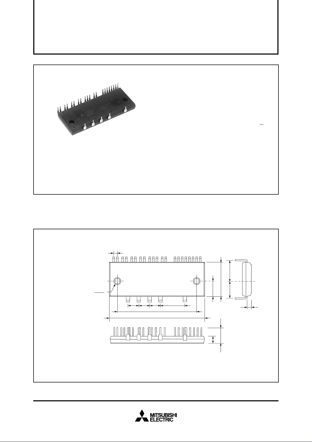
Fig. 1 PACKAGE OUTLINES
2.8
2120192418172516231522141311 121098765432
31
26
11.5
8
N
N
N
13.4 21.4
12.8
22. P 25. W
23. U 26. N
24. V
TERMINALS CODE
1. U
P
4. V
2. V
P1
5. V
3. V
UFB
6. V
UFS
P
P1
2-φ4.5
7. V
8. V
9. W
1
VFB
VFS
P
10. V
11. V
12. V
P1
PC
WFB
101010
67
79
13. V
14. V
15. V
20
WFS
16. CIN 19. U
N1
17. CFO 20. V
NC
18. Fo 21. W
3.8
Aug. 1999
MITSUBISHI SEMICONDUCTOR <Dual-In-Line Package Intelligent Power Module>
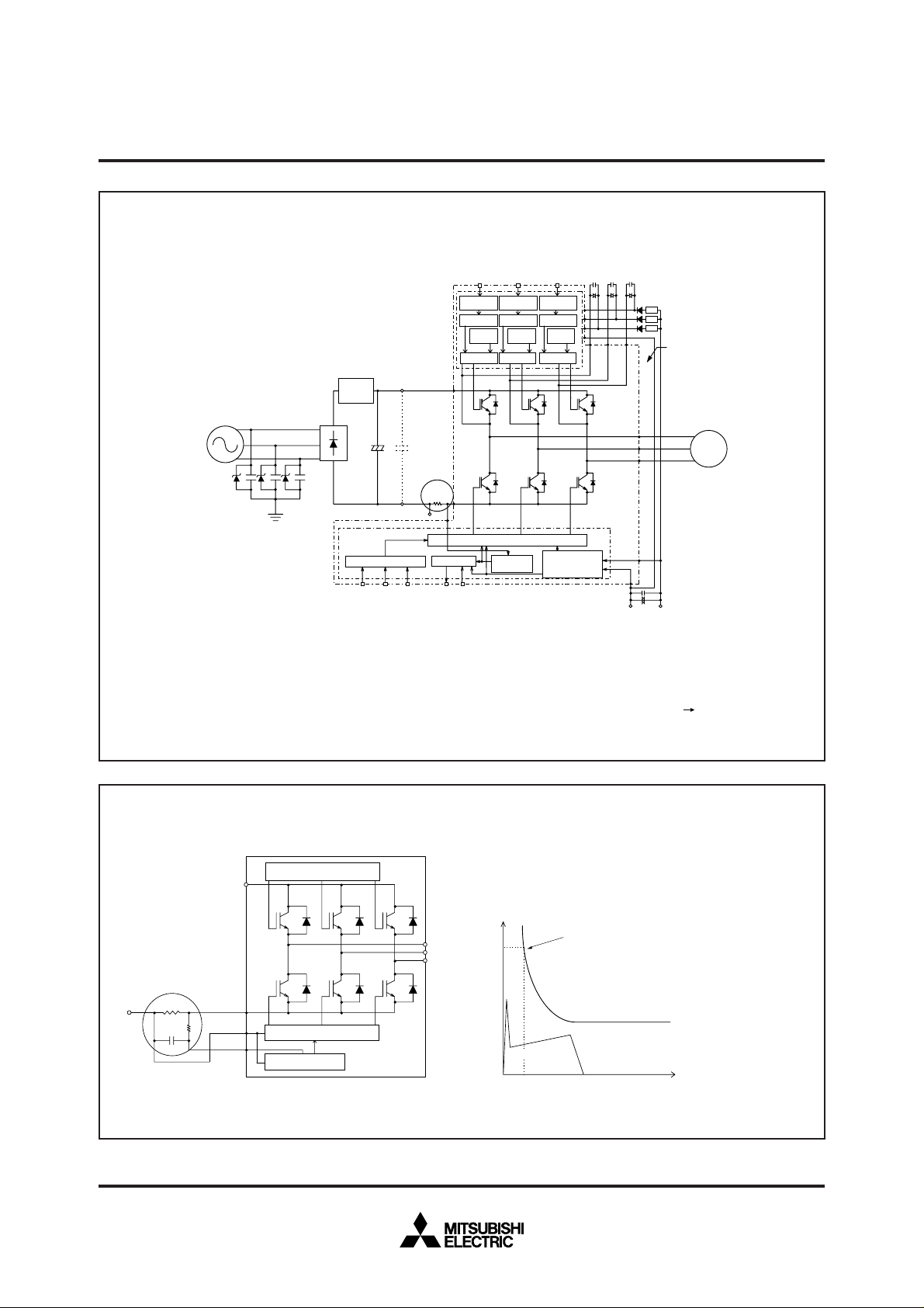
Fig. 2 INTERNAL FUNCTIONS BLOCK DIAGRAM (TYPICAL APPLICATION EXAMPLE)
CBW–
CBV+
CBU–
CBV–
C3 : Tight tolerance, temp-compensated electrolytic type
(Note : The capacitance value depends on the PWM control
scheme used in the applied system).
C4 : 0.22~2µF R-category ceramic capacitor for noise filtering.
Inrush current
limiter circuit
High-side input (PWM)
(5V line) Note 1,2)
Input signal
coditioning
Level shifter
Protection
circuit (UV)
Drive circuit
P
Input signal
Input signal
coditioning
coditioning
Level shifter Level shifter
Protection
Protection
circuit (UV)
circuit (UV)
Drive circuit Drive circuit
CBU+
PS21204
TRANSFER-MOLD TYPE
INSULATED TYPE
CBW+
Bootstrap circuit
For detailed description
of the boot-strap circuit
C4
construction, please
C3
contact Mitsubishi
Electric
(Note 6)
DIP-IPM
AC line input
(Note 4)
C
Z
Z : ZNR (Surge absorber)
C : AC filter (Ceramic capacitor 2.2~6.5nF)
(Note : Additionally, an appropriate line-to line
surge absorber circuit may become necessary
depending on the application environment).
Note1: To prevent the input signals oscillation, an RC coupling at each input is recommended. (see also Fig. 7)
2: By virtue of integrating an application specific type HVIC inside the module, direct coupling to CPU terminals without any opto-coupler or transformer
isolation is possible. (see also Fig. 7)
3: This output is open collector type. The signal line should be pulled up to the positive side of the 5V power supply with approximately 5.1kΩ resistance.
(see also Fig. 7)
4: The wiring between the power DC link capacitor and the P/N1 terminals should be as short as possible to protect the DIP-IPM against catastrophic high
surge voltages. For extra precaution, a small film type snubber capacitor (0.1~0.22µF, high voltage type) is recommended to be mounted close to
these P and N1 DC power input pins.
5: Fo output pulse width should be decided by putting external capacitor between CFO and V
6: High voltage diodes (600V or more) should be used in the bootstrap circuit.
Input signal conditioning
Low-side input (PWM)
(5V line) (Note 1, 2)
Fig. 3
N
1
V
NC
CIN
Fo logic
FOCFO
Fault output (5V line)
(Note 3, 5)
N
Drive circuit
Protection
circuit
NC
H-side IGBT
S
U
V
W
L-side IGBT
Control supply
Under-Voltage
protection
S
V
NC
(15V line)
terminals. (Example : CFO=22nF tFO=1.8ms (Typ.))
Fig. 3 EXTERNAL PART OF THE DIP-IPM PROTECTION CIRCUIT
DIP-IPM
P
H-side IGBTS
External protection circuit
Shunt Resistor
N1
R
C
L-side IGBTS
A
N
NC
V
CIN
B
C
Note1: In the recommended external protection circuit, please select the RC time constant in the range 1.5~2.0µs.
2: To prevent erroneous protection operation, the wiring of A, B, C should be as short as possible.
Drive circuit
Drive circuit
Protection circuit
Short Circuit Protective Function (SC) :
SC protection is achieved by sensing the L-side DC-Bus current (through the external
shunt resistor) after allowing a suitable filtering time (defined by the RC circuit).
When the sensed shunt voltage exceeds the SC trip-level, all the L-side IGBTs are turned
OFF and a fault signal (Fo) is output. Since the SC fault may be repetitive, it is
recommended to stop the system when the Fo signal is received and check the fault.
IC (A)
SC Protection
waveform
Trip Level
w
(µs)
t
U
V
W
Collector current
0
2
AC line output
D
V
M
Aug. 1999

MITSUBISHI SEMICONDUCTOR <Dual-In-Line Package Intelligent Power Module>
PS21204
TRANSFER-MOLD TYPE
INSULATED TYPE
MAXIMUM RATINGS (Tj = 25°C, unless otherwise noted)
INVERTER PART
ConditionSymbol Parameter Ratings Unit
CC
V
VCC(surge)
VCES
±IC
±ICP
PC
Tj
Note 1 : The maximum junction temperature rating of the power chips integrated within the DIP-IPM is 150°C (@ TC ≤ 100°C) however, to in-
Supply voltage
Supply voltage (surge)
Collector-emitter voltage
Each IGBT collector current
Each IGBT collector current (peak)
Collector dissipation
Junction temperature
sure safe operation of the DIP-IPM, the average junction temperature should be limited to T
Applied between P-N
Applied between P-N
C = 25°C
T
C = 25°C, instantaneous value (pulse)
T
C = 25°C, per 1 chip
T
(Note 1)
j(ave) ≤ 125°C (@ TC ≤ 100°C).
450
500
600
15
30
43
–20~+150
CONTROL (PROTECTION) PART
ConditionSymbol Parameter Ratings Unit
D
V
VDB
VCIN
VFO
IFO
VSC
Control supply voltage
Control supply voltage
Input voltage
Fault output supply voltage
Fault output current
Current sensing input voltage
Applied between V
Applied between VUFB-VUFS, VVFB-VVFS,
Applied between UP, VP, WP-VPC, UN, VN,
Applied between FO-VNC
Sink current at FO terminal
Applied between CIN-V
P1-VPC, VN1-VNC
V
WFB-VWFS
W
N-VNC
NC
20
20
–0.5~+5.5
–0.5~V
15
–0.5~V
D+0.5
D+0.5
V
V
V
A
A
W
°C
V
V
V
V
mA
V
TOTAL SYSTEM
Symbol Ratings Unit
CC(PROT)
V
TC
Tstg
Viso
Self protection supply voltage limit
(short circuit protection capability)
Module case operation temperature
Storage temperature
Isolation voltage
Parameter Condition
D = VDB = 13.5~16.5V, Inverter part
V
T
j = 125°C, non-repetitive, less than 2 µs
(Note 2)
60Hz, Sinusoidal, AC 1 minute, connection
pins to heat-sink plate
400
–20~+100
–40~+125
1500
Note 2 : TC MEASUREMENT POINT
Control pins
DIP-IPM
Heat sink boundary
Tc
Power pins
V
°C
°C
rms
V
Aug. 1999

MITSUBISHI SEMICONDUCTOR <Dual-In-Line Package Intelligent Power Module>
THERMAL RESISTANCE
ConditionSymbol Parameter
Rth(j-c)Q
Rth(j-c)F
Rth(c-f)
Junction to case thermal
resistance
Contact thermal resistance
ELECTRICAL CHARACTERISTICS (Tj = 25°C, unless otherwise noted)
INVERTER PART
Symbol Parameter
V
CE(sat)
VEC
ton
trr
tc(on)
toff
tc(off)
ICES
Collector-emitter saturation
voltage
FWDi forward voltage
Switching times
Collector-emitter cut-off
current
Inverter IGBT part (per 1/6 module)
Inverter FWDi part (per 1/6 module)
Case to fin, (per 1 module)
thermal grease applied
Condition
I
VD = VDB = 15V
CIN = 0V
V
C = 15A, Tj = 25°C
C = 15A, Tj = 125°C
I
Tj = 25°C, –IC = 15A, VCIN = 5V
V
CC = 300V, VD = VDB = 15V
C = 15A, Tj = 125°C, VCIN = 5V → 0V
I
Inductive load (upper-lower arm)
on, toff include delay time of the internal control
Note: t
circuit
j = 25°C
CE = VCES
V
T
j = 125°C
T
PS21204
TRANSFER-MOLD TYPE
INSULATED TYPE
Limits
Min.
—
—
—
Min. Typ. Max.
—
—
—
—
—
—
—
—
—
—
Typ. Max.
—
2.85
—
—
0.067
Limits
1.8
2.0
2.2
0.7
0.1
0.4
1.9
0.9
—
—
4.5
—
—
—
—
—
—
—
—
1.0
10
Unit
°C/W
Unit
V
V
µs
mA
CONTROL (PROTECTION) PART
—
—
—
—
4.9
—
0.8
—
3.0
1.0
0.8
2.5
0.8
2.5
Limits
15.0
15.0
4.25
0.50
4.95
0.50
—
1.0
1.2
5.0
—
0.5
—
—
—
—
1.8
1.4
3.0
1.4
3.0
16.5
16.5
8.50
1.00
9.70
1.00
—
2.0
1.8
—
—
0.55
12.0
12.5
12.5
13.0
—
2.0
4.0
2.0
4.0
-6
✕ tFO [F].
Unit
V
V
mA
mA
mA
mA
V
V
V
kHz
µs
V
V
V
V
V
ms
V
V
Symbol Parameter
VD
VDB
Control supply voltage
Control supply voltage
ID
Circuit current
VFOH
VFOL
Fault output voltage
VFOsat
fPWM
tdead
VSC(ref)
PWM input frequency
Allowable deadtime
Short circuit trip level
UVDBt
UVDBr
UVDt
Supply circuit under-voltage
protection
UVDr
tFO
Vth(on)
Vth(off)
Vth(on)
Vth(off)
Fault output pulse width (Note 3)
ON threshold voltage
OFF threshold voltage
ON threshold voltage
OFF threshold voltage
Applied between VP1-VPC, VN1-VNC
Applied between VUFB-VUFS, VVFB-VVFS, VWFB-VWFS
VD = VDB= 15V,
input = OFF
D = VDB= 15V,
V
input = ON
VSC = 0V, FO circuit : 10kΩ to 5V pull-up
SC = 1V, FO circuit : 10kΩ to 5V pull-up
V
SC = 1V, IFO = 15mA
V
C ≤ 100°C, Tj ≤ 125°C
T
Relates to corresponding input signal for blocking arm
shoot-through. –20°C ≤ T
j = 25°C, VD = 15°C (Note 2)
T
Tj ≤ 125°C
FO = 22nF (connected between CFO–VNC)
C
H-side
L-side
Condition
P1-VPC, VN1-VNC
V
VUFB-VUFS, VVFB-VVFS, VWFB-VWFS
VP1-VPC, VN1-VNC
VUFB-VUFS, VVFB-VVFS, VWFB-VWFS
C ≤ 100°C
Trip level
Reset level
Trip level
Reset level
Applied between:
P, VP, WP-VPC
U
Applied between:
N, VN, WN-VNC
U
Min. Typ. Max.
13.5
13.5
0.45
10.0
10.5
10.3
10.8
Note 2: Short circuit protection is functioning only at the low-arms. Please select the value of the external shunt resistor such that the SC trip-
level is less than 25.5 A.
3:Fault signal is output when the low-arms short circuit or control supply under-voltage protective functions operate. The fault output pulse-
FO depends on the capacitance value of CFO according to the following approximate equation : CFO = 12.2 ✕ 10
width t
Aug. 1999

MITSUBISHI SEMICONDUCTOR <Dual-In-Line Package Intelligent Power Module>
MECHANICAL CHARACTERISTICS AND RATINGS
Parameter
Mounting torque
Weight
RECOMMENDED OPERATION CONDITIONS
CC
V
VD
VDB
∆VD, ∆VDB
tdead
fPWM
VCIN(ON)
VCIN(OFF)
Supply voltage
Control supply voltage
Control supply voltage
Control supply variation
Arm shoot-through blocking time
PWM input frequency
Input ON threshold voltage
Input OFF threshold voltage
Mounting screw : M4
Applied between P-N
Applied between V
Applied between VUFB-VUFS, VVFB-VVFS, VWFB-VWFS
For each input signal
C ≤ 100°C, Tj ≤ 125°C
T
Applied between U
Applied between UN, VN, WN-VNC
Condition
Recommended 12kg·cm
Recommended 1.18N·m
ConditionSymbol Parameter
P1-VPC, VN1-VNC
P, VP, WP-VPC
PS21204
TRANSFER-MOLD TYPE
INSULATED TYPE
Limits
0
3
Typ. Max.
—
—
54
Limits
300
15.0
15.0
—
—
5
0~0.65
4.0~5.5
15
1.47
—
400
16.5
16.5
1.0
—
—
Min.
10
0.98
—
Min. Typ. Max.
13.5
13.5
–1
—
Unit
kg·cm
N·m
g
Unit
V
V
V
V/µs
µs
kHz
V
V
Fig. 4 THE DIP-IPM INTERNAL CIRCUIT
N
N
Fo
Fo
NO
V
N
V
W
NVNUN
W
OUT
W
U
OUT
V
CFOCIN
NC
V
GND
CFO
CIN
N1
V
CC
V
LVIC
OUT
U
PC
V
COM
S
V
P
W
IN
HO
P1
V
CC
V
B
V
WFS
V
HVIC 3
WFB
V
COM
S
V
P
V
IN
HO
P1
V
CC
V
B
V
VFS
V
HVIC 2
VFB
V
COM
S
V
P
U
IN
HO
CC
V
P1
V
B
V
UFS
V
HVIC 1
UFB
V
DIP-IPM
N
W
V
U
P
Aug. 1999

MITSUBISHI SEMICONDUCTOR <Dual-In-Line Package Intelligent Power Module>
Fig. 5 TIMING CHARTS OF THE DIP-IPM PROTECTIVE FUNCTIONS
[A] Short-Circuit Protection (Lower-arms only)
(For the external shunt resistance and CR connection, please refer to Fig. 3.)
a1. Normal operation : IGBT ON and carrying current.
a2. Short circuit current detection (SC trigger).
a3. Hard IGBT gate interrupt.
a4. IGBT turns OFF.
a5. FO timer operation starts : The pulse width of the FO signal is set by the external capacitor CFO.
a6. Input “H” : IGBT OFF state.
a7. Input “L” : IGBT ON state, but during the F
a8. IGBT OFF state.
O active signal the IGBT doesn’t turn ON.
PS21204
TRANSFER-MOLD TYPE
INSULATED TYPE
Lower-arms control input
Protection circuit state
Internal IGBT gate
Output current Ic(A)
Sense voltage of the
shunt resistance
Error output Fo
Note : The CR time constant safe guards against erroneous SC fault signals resulting from di/dt generated voltages when the IGBT turns ON.
The optimum setting for the CR circuit time constant is 1.5~2.0µs.
a1
SET
a3
a2
SC
CR circuit time constant DELAY (*Note)
a5
a7
a6
RESET
a4
a8
SC reference voltage
[B] Under-Voltage Protection (N-side, UVD)
a1. Normal operation : IGBT ON and carrying current.
a2. Under voltage trip (UV
a3. IGBT OFF inspite of control input condition.
a4. F
O timer operation starts : The pulse width of the FO signal is set by the external capacitor CFO.
a5. Under voltage reset (UV
a6. Normal operation : IGBT ON and carrying current.
Dt).
Dr).
Control input
Protection circuit state
Control supply voltage V
D
Output current Ic(A)
Error output Fo (N-side only)
UV
SET
Dr
UV
Dt
a2
RESET
a5
a6a1 a3
a4
Aug. 1999

MITSUBISHI SEMICONDUCTOR <Dual-In-Line Package Intelligent Power Module>
PS21204
TRANSFER-MOLD TYPE
INSULATED TYPE
[C] Under-Voltage Protection (P-side, UVDB)
a1. Control supply voltage rises : After the voltage level reachs UVDBr, the circuits start to operate when the next input is applied.
a2. Normal operation : IGBT ON and carrying current.
a3. Under voltage trip (UV
a4. IGBT OFF inspite of control input condition, but there is no F
a5. Under-voltage reset (UV
a6. Normal operation : IGBT ON and carrying current.
Control input
DBt).
O signal output.
DBr).
Protection circuit state
UV
DBr
Control supply voltage V
Output current Ic(A)
Error output Fo
DB
High-level (no fault output)
a1
Fig. 7 RECOMMENDED CPU I/O INTERFACE CIRCUIT
5V line
4.7kΩ
5.1kΩ
SETRESET
UV
DBt
a3
a2 a4
DIP-IPM
RESET
a5
a6
P,VP,WP,UN,VN,WN
U
CPU
Fo
1nF
Note : RC coupling at each input (parts shown dotted) may change depending on the
PWM control scheme used in the application and on the wiring impedances of
the application’s printed circuit board.
1nF
VNC(Logic)
Aug. 1999

MITSUBISHI SEMICONDUCTOR <Dual-In-Line Package Intelligent Power Module>
Fig. 8 TYPICAL DIP-IPM APPLICATION CIRCUIT EXAMPLE
PS21204
TRANSFER-MOLD TYPE
INSULATED TYPE
For detailed description of the boot-strap circuit
construction, please contact Mitsubishi Electric
5V line
C
P
U
U
N
I
T
5V line
15V line
C1: Tight to lerance temp-compensated electrolytic type; C2,C3: 0.22~2 µ F R-category ceramic capacitor for noise filtering
(Note : The capacitance value depends on the PWM control used in the applied system)
V
UFB
C2
C1
V
UFS
V
P1
C3
U
P
C2
V
VFB
C1
V
VFS
V
P1
C3
V
P
C2
V
WFB
C1
V
WFS
V
P1
C3
W
P
V
PC
C3
V
N1
U
N
V
N
W
N
Fo
V
NC
V
IN
COM
V
IN
COM
V
IN
COM
V
CC
U
N
V
N
W
F
o
GND
V
B
CC
HO
V
S
V
B
CC
HO
V
S
V
B
CC
HO
V
S
U
OUT
V
OUT
W
OUT
N
V
NO
CIN
CFO
CFO
FO
)
C4(C
A
CIN
C5
B
DIP-IPM
R1
P
U
V
W
N
Shunt
Resistor
M
C
R
Sh
N1
Note 1 : To prevent the input signals oscillation, an RC coupling at each input is recommended, and the wiring of each input should be as short
as possible. (Less than 2cm)
2:By virtue of integrating an application specific type HVIC inside the module, direct coupling to CPU terminals without any opto-coupler
or transformer isolation is possible.
3:F
O output is open collector type. This signal line should be pulled up to the positive side of the 5V power supply with approximately
5.1kΩ resistance.
4:F
O output pulse width should be decided by connecting an external capacitor between CFO and VNC terminals (CFO). (Example : CFO
= 22 nF → tFO = 1.8 ms (typ.))
5:Each input signal line should be pulled up to the 5V power supply with approximately 4.7kΩ resistance (other RC coupling circuits at
each input may be needed depending on the PWM control scheme used and on the wiring impedances of the system’s printed circuit
board). Approximately a 0.22~2µF by-pass capacitor should be used across each power supply connection terminals.
6:To prevent errors of the protection function, the wiring of A, B, C should be as short as possible.
7:In the recommended protection circuit, please select the R
1C5 time constant in the range 1.5~2µs.
8:Each capacitor should be put as nearby the pins of the DIP-IPM as possible.
9:To prevent surge destruction, the wiring between the smoothing capacitor and the P&N1 pins should be as short as possible. Approxi-
mately a 0.1~0.22µF snubber capacitor between the P&N1 pins is recommended.
Aug. 1999
 Loading...