

Page 1
Pb Solder, Pb Joints, Pb PCA
This product uses lead-free solder
on the circuit boards. For repairing
circuit boards, see "Precautions for
resoldering" in this Service Manual.
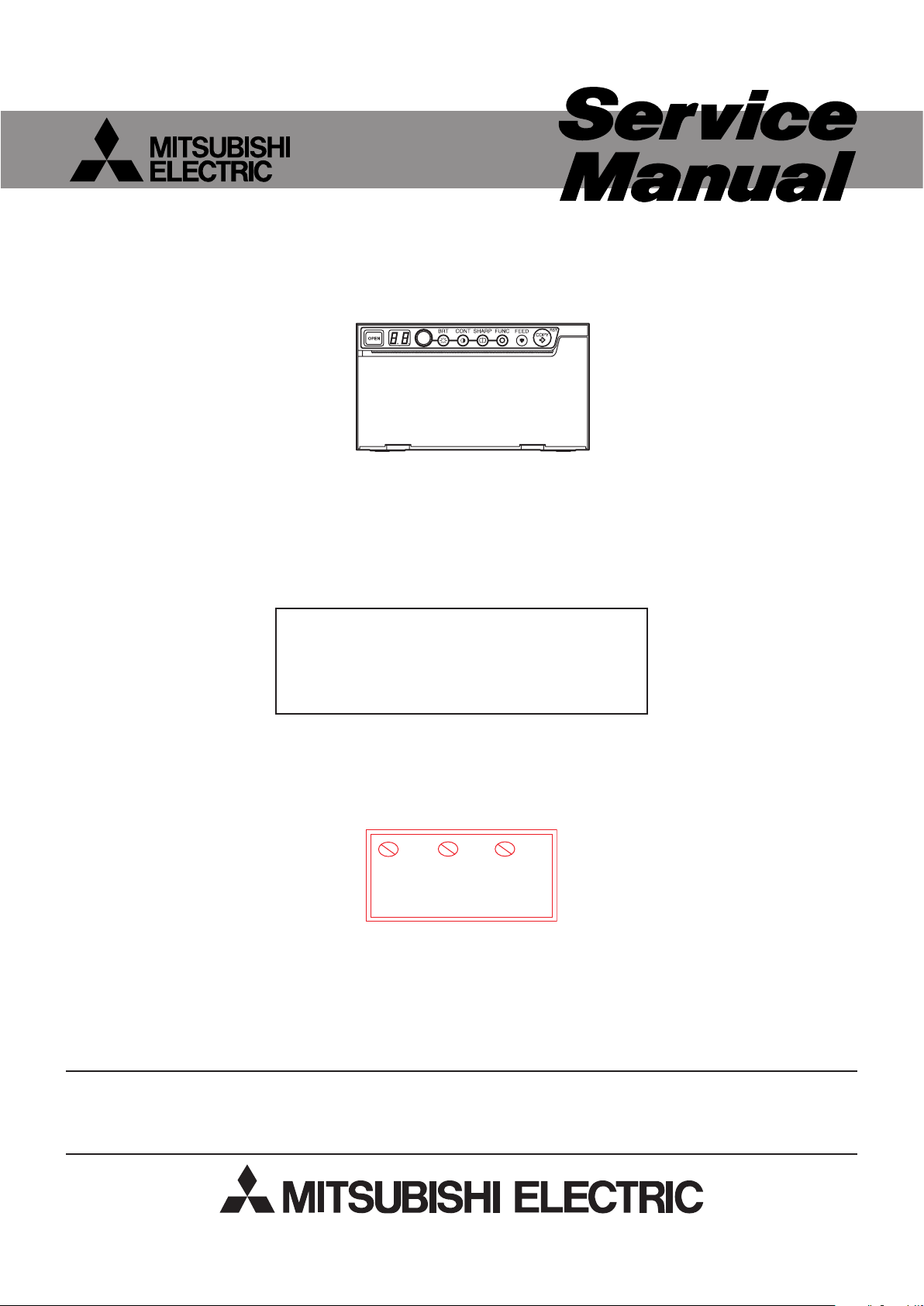
DIGITAL MONOCHROME PRINTER
MODEL
2008
P95DW
This model is RoHS-compliant.
Provide servicing referring to “NOTES
FOR SERVICING RoHS-COMPLIANT
PRODUCTS” described in the service
manual.
Before servicing this chassis, it is important that the service person reads the “SAFETY PRECAUTIONS” and “PRODUCT
SAFETY NOTICE” in this service manual.
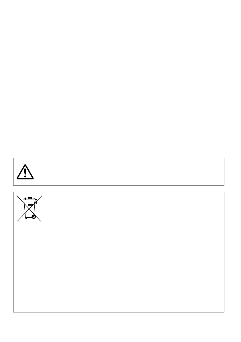
CAUTION
Copyright © 2008 Mitsubishi Electric Corporation All Rights Reserved.
Page 2
NOTES FOR SERVICING RoHS-COMPLIANT PRODUCTS
Parts Name
Model Name
Parts No.
E05R
Mark position
Mark position
Follow the notes and instructions below when servicing RoHS-compliant
products.
1. For RoHS-compliant products, be sure to use RoHS-compliant service parts.
2. Check the presence of <G> marking on the rating plate to distinguish RoHScompliant product from non-RoHS-compliant product.
<G> marking
With <G> marking: RoHS-compliant product
Without <G> marking: Non-RoHS-compliant product
<Sample>
3.LabelsofRoHS-compliantservicepartsbear<G>markingforidenticationpurpose.
<Sample>
4. Don’t use non-RoHS-compliant parts with RoHS-compliant products.
5. Service parts for RoHS-compliant products are listed in the parts catalog contained
in the service manual.
- 2 -
Page 3

SPECIFICATIONS
• Power Supply
• Dot Resolution
• Printing Speed
• Gradations
• Printing Size
•
Connection Terminal
•
Cabinet Dimensions
• Weight
•
Operating conditions
: AC 100 to 240V 50/60Hz,1.5 to 0.8A
: 1280 pixels (H) x 960 pixels (V)(Standard)
(Max.1280 pixels x 5760 pixels)
: Approx.1.9sec.(Standard)
: 256gradations
: 4.0” × 3.0”(100mm × 75mm)(Standard)
(Max.4.0” × 17.7”(100mm × 450mm))
: USB interface (Series ”B” receptacle)
Hi-Speed USB (Ver. 2.0) supported
: 6.1” (W) × 3.3” (H) × 9.4” (D)
154mm (W) × 84.5mm (H) × 239mm (D)
: 2.6kg (5.8lbs)
: Temperature 41 to 104°F (5 to 40°C)
Humidity 20 - 80% RH (No dewing)
• Weight and dimensions shown are approximate.
• Designandspecicationsaresubjecttochangewithoutnotice.
- 3 -
Page 4

CONTENTS
– FILE “COVERPGE” –
NOTES FOR SERVICING RoHS-COMPLIANT PRODUCTS .............................................................................. 2
SPECIFICATIONS ................................................................................................................................................. 3
CONTENTS ........................................................................................................................................................... 4
– FILE “INSTBOOK” –
FEATURES AND FUNCTIONS ............................................................................................................................. 1
INSTALLATION OF PAPER .................................................................................................................................. 2
EXAMPLE OF CONNECTION .............................................................................................................................. 3
ERROR DISPLAY ................................................................................................................................................. 3
STATUS AND MODES .......................................................................................................................................... 5
USE OF CLEANING SHEET ................................................................................................................................ 5
MAINTENANCE .................................................................................................................................................... 6
– FILE “EXPOSED” –
SAFETY PRECAUTIONS ..................................................................................................................................... 1
PRECAUTIONS FOR RESOLDERING ................................................................................................................ 2
PCB LOCATION ................................................................................................................................................... 3
DISASSEMBLY ..................................................................................................................................................... 4
1. Top ASSY ............................................................................................................................................... 4
2. Door ASSY SI ......................................................................................................................................... 4
3. Front ASSY ............................................................................................................................................ 5
4. Main PCB ASSY ..................................................................................................................................... 5
5. Power PCB ASSY .................................................................................................................................. 6
6. Front PCB ASSY / Cutter ....................................................................................................................... 7
7. Print deck ASSY ..................................................................................................................................... 8
8. Solenoide ............................................................................................................................................... 9
9. Motor unit ............................................................................................................................................... 9
10. Platen roller ASSY ................................................................................................................................ 10
11. SP sensor unit(light receiver of paper detector1 / light receiver of paper detector2) ........................... 12
12. SH sensor unit(head position sensor) .................................................................................................. 12
13. SH sensor unit(light emitter of paper detector1) .................................................................................. 13
14. SR sensor unit(Door open / close sensor) ........................................................................................... 13
15. SD sensor unit(light emitter of paper detector2) .................................................................................. 13
16. Head ASSY .......................................................................................................................................... 15
LEAD DRESS ....................................................................................................................................................... 16
– FILE “ADJ” –
SERVICE MODE AND CIRCUIT ADJUSTMENTS ............................................................................................... 1
Service 0 mode .......................................................................................................................................... 2
Service 1 mode .......................................................................................................................................... 4
Adjustmentofpaperdetectionlevel ........................................................................................................... 6
E2PROM INITIALIZATION .................................................................................................................................... 6
Factory out (Perform this process mainly after replacing the Main PCB ASSY.) ....................................... 6
Service ini (Perform this process mainly after replacing the head ASSY.) ................................................. 6
Function clear ............................................................................................................................................. 6
TEST PRINTING ................................................................................................................................................... 7
ELECTRICAL ADJUSTMENT .............................................................................................................................. 8
TEST EQUIPMENT .................................................................................................................................... 8
Power Circuit
1. Primary boost voltage .................................................................................................................... 8
2. Head voltage .................................................................................................................................. 8
– FILE “PARTSLST” –
PACKING PARTS ................................................................................................................................................. 2
LABEL ATTACHING POSITION ........................................................................................................................... 4
PARTS LIST .......................................................................................................................................................... 5
– FILE “EXPLODED” –
EXPLODED VIEW ( CHASSIS ) ................................................................................................................ 2
PARTS LIST ( CHASSIS ) .......................................................................................................................... 3
EXPLODED VIEW ( PRINT DECK ASSY ) ................................................................................................ 6
PARTS LIST ( PRINT DECK ASSY ).......................................................................................................... 7
– FILE “SCHEMATC” –
BLOCK DIAGRAMS
SCHEMATIC DIAGRAMS
- 4 -
Page 5
DIGITAL MONOCHROME PRINTER
MODEL
P95DW
P95DE
OPERATION MANUAL
THIS OPERATION MANUAL IS IMPORTANT
TO YOU.
PLEASE READ IT BEFORE USING YOUR
DIGITAL MONOCHROME PRINTER.
FRANÇAIS DEUTSCHITALIANO
NEDERLANDS
DIGITAL MONOCHROME
ESPAÑOL ENGLISH
PRINTER
This digital monochrome printer complies with the requirements of the
EC Directive 93/42/EEC.
Page 6

Page 7

FOR THE MODEL P91DW(UB) ONLY
WARNING:
In the USA or Canada, use the AC power cord according to the recommendations as
below, in order to comply with UL60601-1 and CAN/CSA C22.2 No. 601.1.
Case 1. Connect to the 120V receptacle of the room or the host equipment.
The AC power cord should be UL or CSA approved and consist of type SJT,
size 16 or 18AWG, length 2.5m or shorter cord with IEC60320-1/C13 type, 125V
10A or higher rating connector and NEMA 5-15 type, 125V 10A or higher rating,
Hospital Grade plug.
Case 2. Connect to the 230V receptacle of the room or the host equipment.
The AC power cord should be UL or CSA approved and consist of type SJT,
size 16 or 18AWG, length 2.5m or shorter cord with IEC60320-1/C13 type, 250V
10A or higher rating connector and NEMA 6-15 type, 250V 10A or higher rating,
Hospital Grade plug.
CAUTION:
Changes or modifications not expressly approved by the party
responsible for compliance could void the user’s authority to operate the
equipment.
NOTE:
This equipment has been tested and found to comply with the limits for a
Class A digital device, pursuant to Part 15 of the FCC Rules.
These limits are designed to provide reasonable protection against harmful interference when the equipment is operated in a commercial environment. This equipment generates, uses, and can radiate radio frequency
energy and, if not installed and used in accordance with the instruction
manual, may cause harmful interference to radio communications.
Operation of this equipment in a residential area is likely to cause harmful
interference in which case the user will be required to correct the interference at his or her own expense.
Information:
This class A digital apparatus complies with Canadian ICES-003.
"CLASSIFIED BY UNDERWRITERS LABORATORIES INC.®
WITH RESPECT TO ELECTRIC SHOCK, FIRE AND MECHANICAL HAZARDS ONLY IN
ACCORDANCE WITH UL60601-1 AND CAN/CSA C22.2 No. 601.1"
FRANÇAIS DEUTSCHITALIANO
NEDERLANDS
ESPAÑOL ENGLISH
Page 8

Indications according to IEC60601-1
1. Functions and intended usage of this product
This product receives signals from diagnostic imaging equipment or a personal computer,
and automatically prints and ejects the received image data on the thermal paper.
2. Classifi cation of this product
• According to the type of protection against electric shock: Equipment energized from an
external electrical power source, Class I equipment
• According to the degree of protection of the applied part against electric shock: - (No
applied part)
• According to the degree of protection against harmful ingress of water: Ordinary
equipment (Enclosed equipment without protection against ingress of water)
• According to the degree of safety of application in the presence of a fl ammable anesthetic
mixture with air or with oxygen or nitrous oxide: Equipment not suitable for use in the
presence of a fl ammable anesthetic mixture with air or with oxygen or nitrous oxide
• According to the mode of operation: Continuous operation with intermittent loading
3. Follow the applicable laws and regulations in your country or region or the hospital rules
when disposing of this product or the accessories or consumables thereof.
DANGER
:
EXPLOSION HAZARD.
DO NOT USE IN THE PRESENCE OF FLAMMABLE ANESTHETICS.
Page 9
CAUTION:
RISK OF ELECTRIC SHOCK DO NOT OPEN.
TO REDUCE THE RISK OF ELECTRIC SHOCK, DO NOT REMOVE COVER (OR
BACK).
NO USER-SERVICEABLE PARTS INSIDE. REFER SERVICING TO QUALIFIED
SERVICE PERSONNEL.
The lightning fl ash with arrowhead symbol, within an equilateral triangle, is
intended to alert the user to the presence of uninsulated "dangerous voltage"
within the product's enclosure that may be of suffi cient magnitude to constitute a
risk of electric shock.
The exclamation point within an equilateral triangle is intended to alert the user
to the presence of important operating and maintenance (servicing) instructions
in the literature accompanying the appliance.
The “Caution, hot surface” symbol indicates that the marked item may be hot
and should not be touched.
The “Nonionizing radiation” symbol
The “OFF/ON” symbol indicates connection to or disconnection from the mains,
at least for mains switches.
The “Equipotentiality” symbol identifi es the terminals connected each other. The
potential of various parts of equipment or of a system is equalized.
The “Alternating current” symbol indicates that the equipment is suitable for
alternating current only.
When you dispose of the unit or accessories, you must obey the law in the relative area
or country and/or regulation in the relative hospital.
: Manufactured on : to be combined with date code YYYY-MM
: Manufacturers Identifi cation (name address)
FRANÇAIS DEUTSCHITALIANO
NEDERLANDS
ESPAÑOL ENGLISH
: Serial number
: Authorised representative in the European Community
Page 10
WARNING:
Install and use this appliance in accordance with the operation manual for safety and
EMC (Electromagnetic Compatibility). If it is not installed and used in accordance with the
operation manual, it may cause interference to other equipment and/or other risk.
To prevent fi re or shock hazard, do not expose this appliance to rain or moisture.
This appliance must be earthed.
In Europe, use the AC power cord according to the recommendations as below.
Connect to the 230 V receptacle of the room or the host equipment.
The AC power cord should be VDE approved and consist of core size 0.75 mm
length 2.5 m or shorter cord with IEC60320-1/C13 type, 250 V 10 A or higher rating
connector and CEE(7)VII type, 250 V 10 A or higher rating plug.
Use the USB cable according to the recommendations as below, in order to comply with
EN60601-1-2.
The USB cable with appropriate plug should be 2 m long or shorter, comply with USB 2.0
standard High speed requirements and USB IF (USB Implementers Forum) approved.
This product is to be employed with medical equipment, just for reference purpose, not for
medical diagnostic purpose.
2
or bigger,
WARNING:
The socket outlet shall be installed near the equipment and shall be easily accessible.
Note: This symbol mark is for EU countries only.
This symbol mark is according to the directive 2002/96/EC Article 10
Information for users and Annex IV, and/or to the directive 2006/66/
EC Article 20 Information for end-users and Annex II.
Your MITSUBISHI ELECTRIC product is designed and manufactured with high quality
materials and components which can be recycled and/or reused.
This symbol means that electrical and electronic equipment, batteries and accumulators,
at their end-of-life, should be disposed of separately from your household waste.
If a chemical symbol is printed beneath the symbol shown above, this chemical symbol
means that the battery or accumulator contains a heavy metal at a certain concentration.
This will be indicated as follows:
Hg: mercury (0,0005%), Cd: cadmium (0,002%), Pb: lead (0,004%)
In the European Union there are separate collection systems for used electrical and electronic products, batteries and accumulators.
Please, dispose of this equipment, batteries and accumulators correctly at your local
community waste collection/recycling centre.
Please, help us to conserve the environment we live in!
Page 11

INSTRUCTIONS FOR MEDICAL USE
<according to the Medical Safety/EMC standard IEC/EN 60601-1-2>
MEDICAL ELECTRICAL EQUIPMENT needs special precautions regarding EMC and needs
to be installed and put into service according to the EMC information provided in the ACCOMPANYING DOCUMENTS.
Portable and mobile RF communications equipment can affect MEDICAL ELECTRICAL
EQUIPMENT.
Technical description
List of all cables and maximum length of the cable and other ACCECCORIES
AC power cord
USB cable
Thermal paper
Maximum length
2.5 m
2 m
Reference page in this operation manual
This page, the previous pages for safety and page 26
for accessories
This page and the previous pages for safety
Page 3 for thermal paper, page 26 for accessories
WARNING:
The use of ACCESSORIES and cables other than those specifi ed, with the exception of ca-
bles sold by the manufacturer of the Model P95DW/P95DE as replacement parts for internal
components, may result in increased EMISSIONS or decreased IMMUNITY of the Model
P95DW/P95DE.
WARNING:
The Model P95DW/P95DE should not be used adjacent to or stacked with other equipment
and that if adjacent or stacked use is necessary, the Model P95DW/P95DE should be observed to verify normal operation in the confi guration in which it will be used.
FRANÇAIS DEUTSCHITALIANO
NEDERLANDS
ESPAÑOL ENGLISH
Page 12
Guidance and manufacturer's declaration - electromagnetic emissions
The Model P95DW/P95DE is intended for use in the electromagnetic environment specified below.
The customer or user of the Model P95DW/P95DE should assure that it is used in such an
environment.
Emissions test
RF emissions
CISPR 11/EN 55011
Compliance
Group 1
Electromagnetic environment - guidance
The Model P95DW/P95DE uses RF energy only for its
internal function. Therefore, its RF emissions are very
low and are not likely to cause interference in nearby
electronic equipment.
RF emissions
CISPR 11/EN 55011
Harmonic emissions
IEC/EN 61000-3-2
Voltage fluctuations/
Class B
Class A
Complies
The Model P95DW/P95DE is suitable for use in all
establishments, including domestic establishments
and those directly connected to the public low-voltage
power supply network that supplies buildings used for
domestic purposes.
flicker emissions
IEC/EN 61000-3-3
Guidance and manufacturer's declaration - electromagnetic immunity
The Model P95DW/P95DE is intended for use in the electromagnetic environment specified below.
The customer or user of the Model P95DW/P95DE should assure that it is used in such an
environment.
Immunity test
Electrostatic
discharge (ESD)
IEC/EN 61000-4-2
Electrical fast
transient/burst
IEC/EN 61000-4-4
Surge
IEC/EN 61000-4-5
IEC/EN 60601
test level
±6 kV contact
±8 kV air
±2 kV for power
supply lines
±1 kV for input
/output lines
±1 kV line(s) to
line(s)
±2 kV line(s) to
earth
Compliance
level
±6 kV contact
±8 kV air
±2 kV for power
supply lines
±1 kV for input
/output lines
±1 kV line(s) to
line(s)
±2 kV line(s) to
earth
Electromagnetic environment - guidance
Floors should be wood, concrete or
ceramic tile. If floors are covered with
synthetic material, the relative humidity
should be at least 30%.
Mains power quality should be that of a
typical commercial or hospital
environment.
Mains power quality should be that of a
typical commercial or hospital
environment.
Voltage dips, short
interruptions and
voltage variations
on power supply
input lines
IEC/EN 61000-4-11
Power frequency
(50/60 Hz)
magnetic field
IEC/EN 61000-4-8
< 5% U
T
(> 95% dip in UT)
for 0.5 cycle
40% U
T
(60% dip in UT)
for 5 cycles
70% U
T
(30% dip in UT)
for 25 cycles
< 5% U
T
(> 95% dip in UT)
for 5 sec.
3 A/m
< 5% U
T
(> 95% dip in UT)
for 0.5 cycle
40% U
T
(60% dip in UT)
for 5 cycles
70% U
T
(30% dip in UT)
for 25 cycles
< 5% U
T
(> 95% dip in UT)
for 5 sec.
3 A/m
Mains power quality should be that of a
typical commercial or hospital
environment. If the user of the Model
P95DW/P95DE requires continued
operation during power mains
interruptions, it is recommended that the
Model P95DW/P95DE be powered from
an uninterruptible power supply or a
battery.
Power frequency magnetic fields should
be at levels characteristic of a typical
location in a typical commercial or
hospital environment.
NOTE: UT is the a.c. mains voltage prior to application of the test level.
Page 13
Guidance and manufacturer's declaration - electromagnetic immunity
The Model P95DW/P95DE is intended for use in the electromagnetic environment specified below.
The customer or user of the Model P95DW/P95DE should assure that it is used in such an
environment.
Immunity test
Conducted RF
IEC/EN 61000-4-6
Radiated RF
IEC/EN 61000-4-3
IEC/EN 60601
test level
3 Vrms
150 kHz to 80
MHz
3 V/m
80 MHz to 2.5
GHz
Compliance
level
3 Vrms
3 V/m
Electromagnetic environment - guidance
Portable and mobile RF communications
equipment should be used no closer to
any part of the Model P95DW/P95DE,
including cables, than the recommended
separation distance calculated from the
equation applicable to the frequency of
the transmitter.
Recommended separation distance
d=1.2√P
d=1.2√P 80 MHz to 800 MHz
d=2.3√P 800 MHz to 2.5 GHz
where P is the maximum output power
rating of the transmitter in watts (W)
according to the transmitter manufacturer
and d is the recommended separation
distance in meters (m).
Field strengths from fixed RF
transmitters, as determined by an
electromagnetic site survey,
a
should be
less than the compliance level in each
frequency range.b
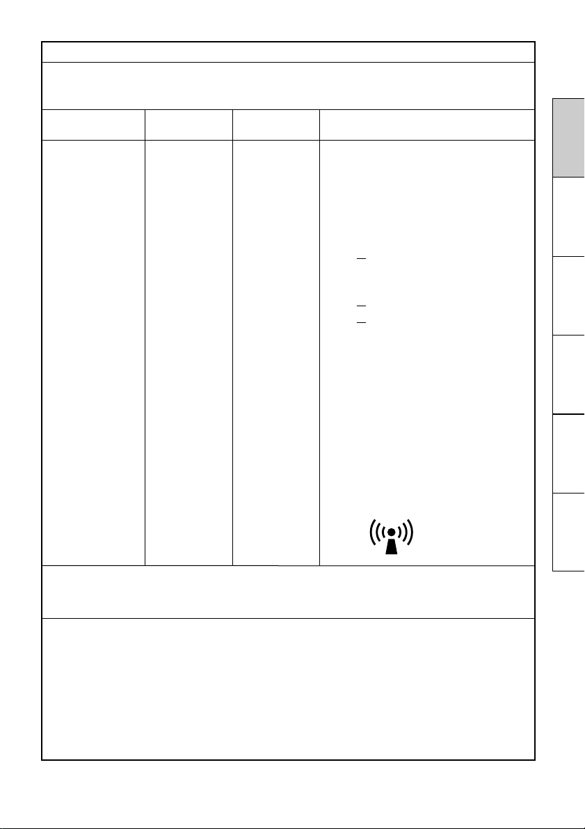
Interference may occur in the vicinity of
equipment marked with the following
symbol:
FRANÇAIS DEUTSCHITALIANO
NEDERLANDS
NOTE1. At 80 MHz and 800 MHz, the higher frequency range applies.
NOTE2. These guidelines may not apply in all situations. Electromagnetic propagation is
affected by absorption and reflection from structures, objects and people.
a
Field strengths from fixed transmitters, such as base stations for radio (cellular/cordless)
telephones and land mobile radios, amateur radio, AM and FM radio broadcast and TV
broadcast cannot be predicted theoretically with accuracy. To assess the electromagnetic
environment due to fixed RF transmitters, an electromagnetic site survey should be
considered. If the measured field strength in the location in which the Model P95DW/P95DE
is used exceeds the applicable RF compliance level above, the Model P95DW/P95DE
should be observed to verify normal operation. If abnormal performance is observed,
additional measures may be necessary, such as reorienting or relocating the Model
P95DW/P95DE.
b
Over the frequency range 150 kHz to 80 MHz, field strengths should be less than 3 V/m.
ESPAÑOL ENGLISH
Page 14
Recommended separation distances between
portable and mobile RF communications equipment and the Model P95DW/P95DE
The Model P95DW/P95DE is intended for use in an electromagnetic environment in which radiated
RF disturbances are controlled. The customer or the user of the Model P95DW/P95DE can help
prevent electromagnetic interference by maintaining a minimum distance between portable and
mobile RF communications equipment (transmitters) and the Model P95DW/P95DE as
recommended below, according to the maximum output power of the communications equipment.
Rated maximum output
power of transmitter
W
0.01
0.1
1
10
100
For transmitters rated at a maximum output power not listed above, the recommended
separation distance d in meters (m) can be estimated using the equation applicable to the
frequency of the transmitter, where P is the maximum output power rating of the transmitter in
watts (W) according to the transmitter manufacturer.
NOTE1. At 80 MHz and 800 MHz, the separation distance for higher frequency range applies.
NOTE2. These guidelines may not apply in all situations. Electromagnetic propagation is
affected by absorption and reflection from structures, objects and people.
Separation distance according to frequency of transmitter
150 kHz to 80 MHz
d=1.2√P
0.12
0.38
1.2
3.8
12
m
80 MHz to 800 MHz
d=1.2√P
0.12
0.38
1.2
3.8
12
800 MHz to 2.5 GHz
d=2.3√P
0.23
0.73
2.3
7.3
23
Safety Notices for use in combination with other devices
1. All the equipments connected to this unit shall be certifi ed according to Standard
IEC60601-1, IEC60950-1, IEC60065 or other IEC/ISO Standards applicable to the equipments.
2. When this unit is used together with other equipment in the patient area*, the equipment shall be either powered by an isolation transformer or connected via an additional
protective earth terminal to system ground unless it is certifi ed according to Standard
IEC60601-1.
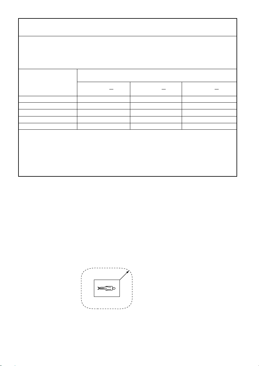
* Patient Area
R1.5m
3. The leakage current could increase when connected to other equipment.
Page 15

1
CONTENTS
CONTENTS .................................................................. 1
PRECAUTIONS ..................................................... 2 - 5
UNPACKING ................................................................ 6
FEATURES AND FUNCTIONS ............................... 7 - 8
Front Panel ..........................................................................................7
Rear Panel ........................................................................................... 8
INSTALLATION OF PAPER .................................9 - 10
EXAMPLE OF CONNECTION ....................................11
PRINTING ...........................................................12 - 13
ADJUSTMENT OF PRINT PICTURE .................14 - 16
SETTING FUNCTION MODE ............................. 17 - 19
ERROR DISPLAY ............................................... 20 - 22
STATUS AND MODES ............................................... 23
USE OF CLEANING SHEET ..................................... 24
MAINTENANCE ......................................................... 25
SPECIFICATIONS ..................................................... 26
FRANÇAIS DEUTSCHITALIANO
NEDERLANDS
ESPAÑOL ENGLISH
1
Page 16

2
PRECAUTIONS
In the interest of safety, please observe the following
precautions:
POWER REQUIREMENT
This digital monochrome printer is designed for operation
on 100-240V AC 50/60Hz. Never connect to any outlet
or power supply having a different voltage or frequency.
PROTECTIVE MEASURES
IF ABNORMALITIES ARISE, . . .
Use of the unit during emission of smoke or abnormal
sounds (without adopting countermeasures) is dangerous. In such a case, unplug the power cord from the
source outlet immediately, and request maintenance
services from the sales dealer.
NEVER INSERT ANY OBJECT INTO THE UNIT
Foreign objects of any kind inserted into this unit constitute a safety hazard and can cause extensive damage.
If any object should be inserted into the unit, unplug the
power cord, then contact the sales dealer.
DO NOT PLACE ANYTHING ON THE UNIT
Heavy objects placed on the unit can cause damage or
obstruct proper ventilation.
PROTECT THE POWER CORD
Damage to the power cord may cause fi re or shock haz-
ard. When unplugging, hold by the plug only and remove
carefully.
Never put heavy objects on the power cord. The cord
may be damaged causing a fi re or electric shock.
DO NOT PLACE WATER CONTAINERS ON THE UNIT
Do not place fl ower vases, and other water-holding con-
tainers on the unit. If, for some reason, water seeps to
the inside of the unit, unplug the power cord from the
source outlet, and contact the sales dealer. If used without corrective measures, the unit may be damaged.
WARNING : THIS APPARATUS MUST BE EARTHED.
AVERTISSEMENT : CET APPAREIL DOIT ETRE MIS A
LA TERRE.
This equipment is classifi ed as class , according to the
type of protection against electric shock.
DO NOT REMOVE THE CABINET
Touching internal parts is dangerous or may lead to malfunction. Contact the sales dealer to carry out internal
checks and/or adjustments. Before opening the cover to
clear a paper jam, etc., be sure to disconnect the power
cord plug.
DO NOT ATTACH A SCREW MORE THAN 6 MM
LONG ON THE BOTTOM
If a screw more than 6 mm long is attached on the bottom of the printer, it may cause internal damage.
PROTECT AGAINST DEW FORMATION
In extremely cold regions, if the unit is moved quickly
from an extremely cold place to a warmer one, dew is
likely to be formed. If dew is formed, printing is not possible.
OPERATING AMBIENT TEMPERATURE RANGE
The operating ambient temperature range is 5°C-40°C
(41°F-104°F), and humidity of 20-80%.
BE CAREFUL AROUND PRINT PAPER EXIT SLOT
Do not insert your hand or any material into the paper
exit slot during printing.
Do not touch the cutter blade inside the paper exit slot.
Otherwise, your fi nger will be injured.
DO NOT TOUCH THE THERMAL HEAD AND CUTTER
Do not touch the thermal head (located inside the unit)
and the cutter blade.
The thermal head is heated to high temperature.
This may cause injury.
INSTALLATION LOCATIONS
MAINTAIN GOOD VENTILATION
Ventilation slots and holes are provided on sides of this
unit.
Place the unit on a hard and level surface and locate at
least 4" (10 cm) from walls to ensure proper ventilation.
SUITABLE LOCATIONS
Avoid shaky places or hot-springs areas where hydrogen
sulfi de and acidic ions are likely to be generated.
AVOID PLACES WITH HIGH HUMIDITY AND DUST
Do not place the unit at locations with high humidity and/
or dust. They can cause extensive damage.
Avoid places where the unit is likely to contact oily fumes
and vapors.
AVOID PLACES LIKELY TO BE EXTREMELY HOT
Places exposed to direct sunlight, or near heating
appliances can attain extremely high temperatures,
which may deform the cabinet, or can become a prime
cause of damage.
SET THE UNIT ON A FLAT SURFACE
Do not use the unit when inclined ±10° in vertical or horizontal direction, or in an unstable place.
Uneven surfaces may disturb paper feeding or ventilation, or affect the performance of the unit.
2
Page 17

FOR LONG OPERATING LIFE
UNSUITABLE MATERIALS FOR THE UNIT
Many plastic components are used in the unit.
Coat fl aking and deformation are likely to occur if the
unit is wiped with chemical dusters, benzine, thinner or
any other solvent, if rubber or PVC items are left in contact with the unit for extended duration, or if the unit is
sprayed with insecticide.
CARE OF THE CABINET
Unplug and clean with a soft cloth slightly moistened with
a mild soap and water solution. Allow to dry completely
before operating. Never use petroleum base solutions or
abrasive cleaners.
HEAD ABRASION
The thermal head, like the video head, wears out.
When it is abraded, it becomes hard to print out fi ne
details of the picture. In such a case, it is necessary to
replace the thermal head. Consult with the sales dealer
for replacing the head.
THERMAL PAPER
Thermal papers listed in the page of SPECIFICA-
TIONS are available.
When the remaining length of the paper is about 8"
(20 cm), a color belt appears at the paper end.
Prepare for replacement of the paper. If the remaining
paper length is less than 8" (20 cm), printing becomes
uneven due to the uneven paper core surface.
When the Printed paper is touched by wet hand, the
print may be discolored.
When the paper runs out during printing, the printing
operation stops and “EP” is displayed by the indicator
on the front panel. Install new paper at this time.
Store the printed paper in a place with low humidity
free from a direct sunlight.
If the paper absorbs non-volatile organic solvents (al-
cohol, ester, katone, etc.) the print may be discolored.
Particularly, if the paper comes in contact with soft
vinyl chloride such as a transparent tape, it quickens
discoloration.
Do not use paper other than the specifi ed types.
WHEN A DEFECT IS FOUND
If you detect smoke or other smell from the unit, disconnect immediately the power cord plug from a wall socket
and ask the agent for repair. It may be dangerous to operate the unit under these conditions.
CONNECTION DEVICES
Read thoroughly Operating Precautions of the instruction booklets for the devices connected with the digital
monochrome printer.
Do not disconnect the power cord during printing.
CAUTION ON RELOCATING
When transporting this unit, make sure it is not likely to
be subjected to impacts. They can be a prime cause for
damage. Further, make sure to disconnect the power
cord from the power outlet, and the cables from the connected devices.
UNPLUG THE POWER CORD DURING A LONG
ABSENCE
Turn off the MAIN power switch and unplug the power
cord during a long absence.
Immediately after the paper is replaced, 2-3 images
may be printed with a blank part due to hand’s dust or
oil.
Avoid direct sunlight or places near heaters, etc., and
store the paper in a place with 30°C (86°F) or lower
temperature and 35-80% RH.
When the paper is rapidly transferred from a cool
place to a hot place, a vapor or a dew is generated
on the paper surface causing paper jam or degraded
printing quality.
A fi nger print or dust on the paper surface may de-
grade the printing quality.
Note:
Mitsubishi brand thermal paper is specially treated with
an anti-static coating against thermal head damage
caused by static-electricity discharge.
The use of non-treated paper may cause premature
head failure in your product.
FRANÇAIS DEUTSCHITALIANO
NEDERLANDS
ESPAÑOL ENGLISH
3
Page 18

SAFETY TECHNICAL CHECKS
Periods: According to the recommendations of the manufacturer of medical device.
Scope: a) Visual check
Housing, cables, operator controls, readout device (displays, LED etc.), labels,
accessories, instruction manual.
b) Function test
Performance check acc. instruction manual, also unity and applicability of set
and accessory test.
c) Electrical check
Safety electrical test of the confi guration in accordance with EN60601-1.
“ In the interest of safety, avoid the handling of liquids beside the set.”
RESPONSIBILITY OF THE MANUFACTURER
The manufacturer, assembler, installer or importer considers himself responsible for the effects on
safety, reliability and performance of the EQUIPMENT only if:
– assembly operations, extensions, re-adjustments, modifi cations or repairs are carried out by persons
authorized by him, and
– the electrical installation of the relevant room complies with the IEC requirements
– the EQUIPMENT is used in accordance with the instructions for use.
• Any service after expiration of the warranty period will be chargeable. Consult your dealer for advice.
TECHNICAL DESCRIPTION
The supplier will make available on request such circuit diagrams, component part lists, descrip-
tions, calibration instructions or other information which will assist the USER’s appropriately qualifi ed
technical personnel to repair those parts of the EQUIPMENT which are classifi ed by the manufac-
turer as repairable.
The use of ACCESSORY equipment not complying with the equivalent safety requirements of this
equipment may lead to a reduced level of safety of the resulting system. Consideration relating to
the choice shall include:
– use of the accessory in the PATIENT VICINITY
– evidence that the safety certifi cation of the ACCESSORY has been performed in accordance with
the appropriate EN60601-1 and/or EN60601-1-1 harmonized national standard.
The transportation and storage environmental conditions are:
Temperature : -20°C - +60°C (-4°F - +140°F)
Humidity: 90%RH or less at 40°C (104°F)
Atmospheric pressure : 50 kPa - 106 kPa
Note : The above transportation environmental conditions indicate the storage environmental con-
ditions during transport.
4
Page 19

PRODUCT OUTLINE
The digital monochrome printer P95DW/P95DE uses the thermal printing system. This printer is able
to print digital grayscale images on the thermal paper. This printer is connected to a host computer via
USB interface. Digital images such as CT, MRI, ultrasound, and CR images transmitted from the host
computer is printed via USB interface.
This printer creates prints electronically (mainly in image processing and printing processing), not optically or chemically.
INTENDED USE
The digital monochrome printer P95DW/P95DE is intended for use as a hard copy device for an image
generated by a diagnostic imaging equipment.
This product is intended to be used together with medical equipment and to be used for reference purpose, not for diagnostic purpose.
FRANÇAIS DEUTSCHITALIANO
NEDERLANDS
ESPAÑOL ENGLISH
5
Page 20
3
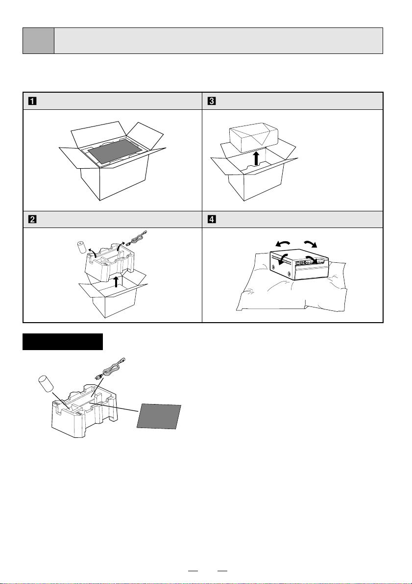
Take the unit out of the box by the following procedures. Make sure to check the
contents.
UNPACKING
Open the top of the box.
Remove
the cushion above the unit.
Accessories
Thermal paper
AC power cord
Take the unit out of the box carefully.
• Make sure to
keep the unit
horizontal.
Unwrap the unit.
Cleaning sheet
Operation manual
Printer driver (1 CD-ROM)
USB cable
6
Page 21
4
FEATURES AND FUNCTIONS
Front Panel
FRANÇAIS DEUTSCHITALIANO
OPEN button
Press to open the door.
Indicator
Displays printer status. See pages 12,
15, 16 and 18 to 23.
Adjustment dial
Changes the settings of each function.
See pages 14, 15 and 17.
BRT (brightness) button
Press this button and then turn the
adjustment dial to adjust the brightness
of the print images. See page 14.
CONT (contrast) button
Press this button and then turn the
adjustment dial to adjust the contrast of
the print images. See page 14.
SHARP (sharpness) button
Press this button and then turn the
adjustment dial to adjust the sharpness
of the print images. See pages 12 and
14.
FUNC (function) button
Press this button and then turn the
adjustment dial to select the function
mode. See pages 16 and 17.
FEED button
Button to advance the paper. See pages
12 and 13.
COPY/RST (restart) button
Button to print additional copies of
previous print-out. You can restart the
printer by pressing and holding down the
COPY/RST button for about 2 seconds.
See pages 12 and 16.
Print exit/Cutter
Printed paper will come out through this
slot. / Cut the printed paper here. See
pages 9, 12 and 24.
NEDERLANDS
ESPAÑOL ENGLISH
7
Page 22
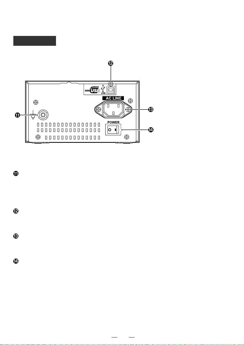
Rear Panel
Potential equalization terminal
This is used to equalize the potential of
the equipment connected to this unit.
For details refer to the installation
instruction of equipment to be connected.
USB terminal
Connects to the device equipped with a
USB interface. See page 11.
Power terminal (AC LINE)
Connect the power cord to this terminal.
See page 11.
Power switch (POWER)
Main power switch. See pages 12 and 24.
8
Page 23
5
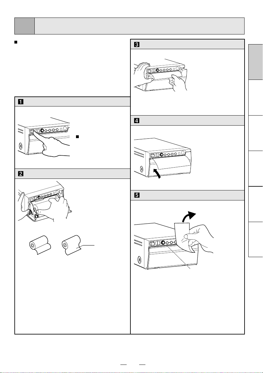
INSTALLATION OF PAPER
Moisture, fi ngerprints or dust on the
paper surface may cause a noise
at printing or deterioration in print
quality. Follow the procedure to
prevent fi ngerprint or dust on the
paper surface.
Open the door.
•
Press the OPEN
button.
The door opens.
Load the paper roll.
• Place the paper roll
in the printer.
Pull out the paper end.
• Pull out the fi rst 15-
20cm (6 in. - 9 in.)
of the paper to
remove any slack
in the roll.
Close the door.
FRANÇAIS DEUTSCHITALIANO
Cut the paper end.
NEDERLANDS
printing side
INCORRECT
Note: The printing surface is the outside.
Place the paper with the thermsensitive side (printing side) up.
When the paper roll is placed in-
versely, images can not be printed.
CORRECT
cutter
•
Cut the paper end with the cutter by
pulling the paper upwards against the
cutter blade.
9
ESPAÑOL ENGLISH
Page 24
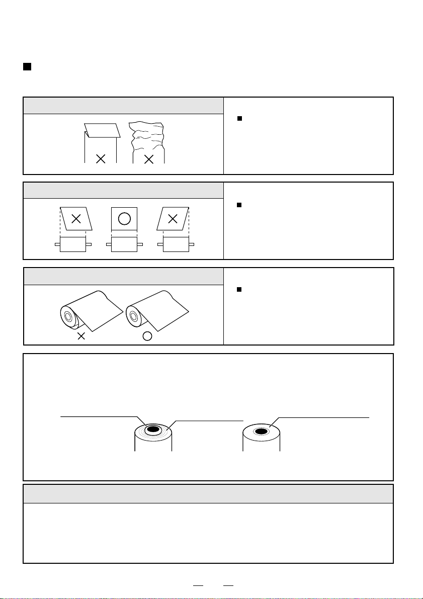
When setting the paper, observe the following precautions to prevent
paper jam.
Do not use defective paper.
Do not use bent or wrinkled paper.
Adjust the paper position correctly.
When the paper is fed out skewed
from the print exit, adjust the paper
position so that it is fed out straight.
Do not allow slack in the paper roll.
Set the paper tightly to remove any
slack.
If the side of the print paper is uneven or the core is sticking out, the amount of paper
feeding after printing may vary.
When the side of paper is uneven or the core is sticking out, install the print paper after
making the paper side even.
The core is sticking out.
INCORRECT
The paper is uneven.
CORRECT
Make the paper side even.
CAUTION
• Keep the high-density paper away from fi ngerprint, dust or moisture when storing it.
• Do not touch the rubber roller. Do not stain or damage the roller surface.
• Do not touch the thermal head (located behind the cutter). During printing, the thermal
head temperature is high.
• Do not touch the cutter blade.
10
Page 25
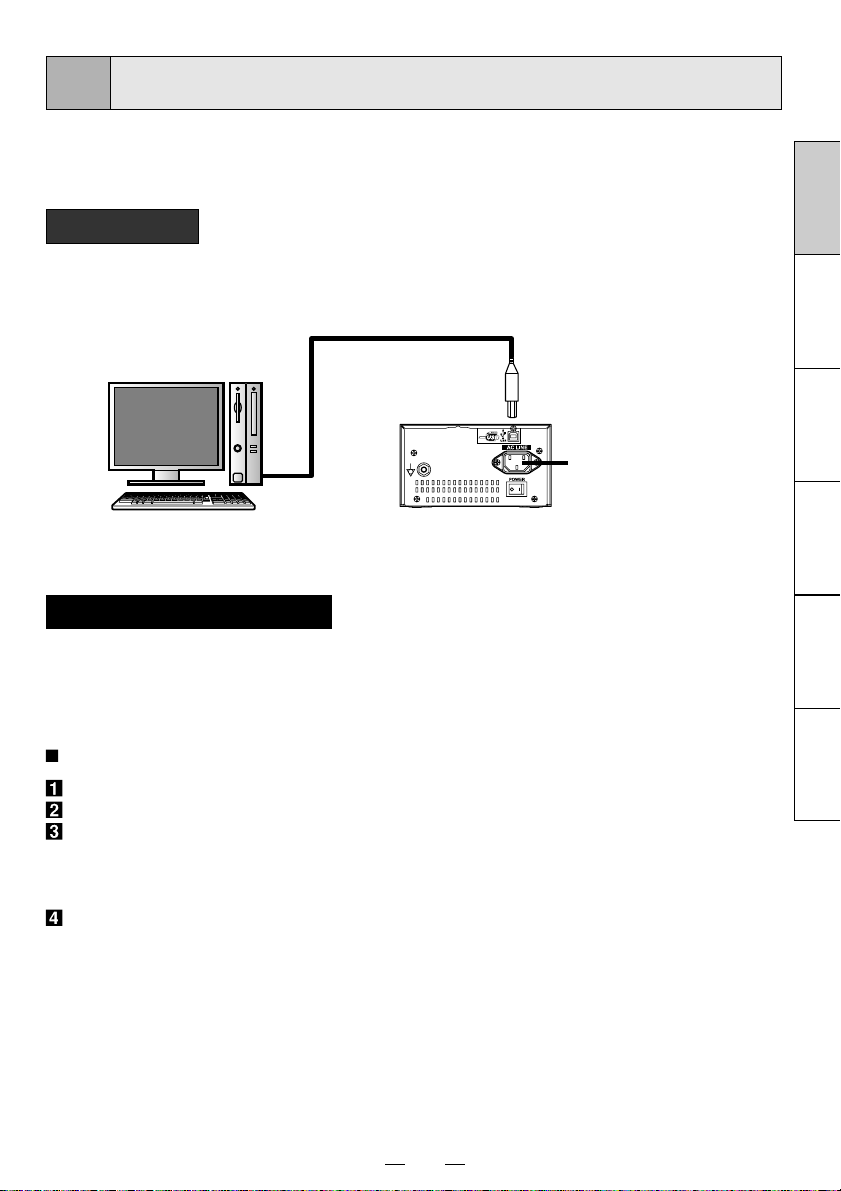
6
EXAMPLE OF CONNECTION
Connecting to various equipment with USB interface such as
medical equipment and personal computer.
Connection
Connect the digital monochrome printer with PC or medical
equipment through a USB cable.
Personal computer or
medical equipment
To USB terminal
Connect
Power cord
Rear panel
Installing printer driver
Printer driver is required to print the data from a personal computer connected with this
printer.
The printer driver for Windows® is supplied with this printer.
Refer to the “Read me” for installing the printer driver in the CD-ROM supplied with this unit.
How to open the ReadMe fi le
Install the CD-ROM in the CD-ROM drive on your PC.
Double-click on the CD-ROM icon.
Double-click on the ReadMe_E.pdf.
Adobe® Reader® or Adobe® Acrobat® Reader® is required to open ReadMe_E.pdf fi le.
You can download Adobe Reader and Acrobat Reader free from the Web site of Adobe
Systems Incorporated (http://www.adobe.com/).
Install the printer driver by following the instruction in the fi le.
Windows is the registered trademark of Microsoft Corporation in the U.S.A. and other
countries.
Adobe, Acrobat Reader and Adobe Reader are registered trademark of Adobe Systems
Incorporated.
FRANÇAIS DEUTSCHITALIANO
NEDERLANDS
ESPAÑOL ENGLISH
11
Page 26
7
PRINTING
Printing method
Turn on the power.
• Press the
POWER
switch on the
rear panel to
turn on the
power.
Print a picture displayed on the screen.
Print a picture with an application
software. The image data is transferred
through USB interface.
Copy Printing
You can set the number of copies by pressing
the COPY button on the front panel. (Setting
range : 1 to 200)
You can copy the same picture as many times
as you desire until a new image data is printed.
The set number of copy printing and the number
of the remainings are displayed on the indicator
as shown right.
The number of copy print setting is not
memorized.
When pressing the SHARP button during copy
printing, continuous printing is enabled.
Cancel of Copy Printing
When pressing the FEED button during copy
printing, the copy printing is cancelled upon
completion of the current copy.
Cut the printed paper.
• Cut the printed
paper with the
cutter by
tearing off the
paper in the
upper right
direction.
cutter
• Do not pull the paper in the horizontal
direction. The paper inside the unit may
be displaced and printing performance
may not be correct.
Indicator
Number of copy printing /
remainings
1 - 99
100 - 199
Continuous printing
200
12
Page 27
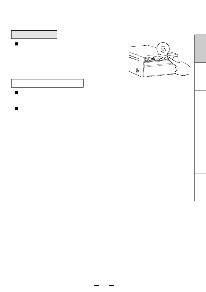
Paper Feeding
To advance the paper, press the FEED button on the
front panel.
Precautions on Printing
When dark pictures are printed repeatedly, the printer may go into overheat condition.
The printer status indicator will fl ash during overheat condition. This is normal case.
The printer will cool down before it starts printing again.
Avoid pulling out or holding the paper during printing or copying to prevent paper jam.
Do not touch the paper until printing or copying fi nishes.
FRANÇAIS DEUTSCHITALIANO
NEDERLANDS
13
ESPAÑOL ENGLISH
Page 28

8
ADJUSTMENT OF PRINT PICTURE
Adjustment of Brightness, Contrast and Sharpness
You can make fi ne adjustment of brightness, contrast and
sharpness of the picture to be printed.
Control panel
• For adjustment, use the BRT “ ”, CONT “ ” or SHARP “ ” button, and the
adjustment dial “ ”.
Press the BRT, CONT or SHARP button.
Press the BRT button “ ” to adjust
the printer brightness.
• The BRT indicator lights up.
• Adjust brightness with adjustment
dial.
Press the CONT button “ ” to
adjust the contrast.
• The CONT indicator lights up.
• Adjust contrast with adjustment dial.
Press the SHARP button “ ” to
adjust the sharpness.
• The SHARP indicator lights up.
• Adjust sharpness with adjustment
dial.
14
Page 29

Change the setting.
Store the set value.
• Turn the dial clockwise
to increase the value.
• Turn the dial
counterclockwise to
decrease the value.
The setting value is displayed by the
indicator.
(example)
Setting range is -19 to +19 for brightness
and contrast and 0 to 15 for sharpness.
Press the (BRT, CONT, or SHARP)
button again to memorize the value.
The memorized value will not be lost
even when the power is turned off.
FRANÇAIS DEUTSCHITALIANO
NEDERLANDS
15
ESPAÑOL ENGLISH
Page 30

Automatic restoration to the standby status from the adjustment or setting mode
Whenever the front dial and buttons are untouched for more
than 20 seconds during adjustment, the printer automatically
returns to the standby status (Indicator display : ).
In this case, the new value is not memorized and the setting
goes back to the previous value.
Resetting the values
You can reset the values of printer brightness, printer
contrast, sharpness and function mode settings.
Turn off the power.
While pressing the FUNC button, turn on the power.
The display by the indicator changes from to , and the values are reset to the
default setting.
Restarting the printer
You can restart the printer by pressing and holding down the
COPY/RST button for about 2 seconds.
When the printer restarts, the ongoing printing is cancelled,
the number of printings is reset and the printer returns to the
standby status.
The values set by the front buttons are not reset.
16
Page 31

9
SETTING FUNCTION MODE
Function mode
In this mode, the initial value setting of each function can be
changed. Each time the FUNC button is pressed, the mode is
switched as follows.
Functions
Stand-by status
Gamma curve setting
Adjustment dial lock setting
Indicator brightness setting
FRANÇAIS DEUTSCHITALIANO
Setting the function mode
By turning the adjustment dial, you can change the value
setting for each function mode. Press the FUNC button again
to memorize the new setting. The set values will not be lost
even when the power is turned off.
17
NEDERLANDS
ESPAÑOL ENGLISH
Page 32

Gamma curve setting
Indicator
• Gamma ( ) curve selection (relation between the density and
the brightness of the image) to obtain an optimum density depending on the source device. Five options are available.
Adjustment dial lock setting
Indicator
• You can select whether or not to lock the adjustment dial
functions.
: The adjustment dial is activated.
: The adjustment dial does not function. When the adjust-
ment dial is turned, an alarm sounds once. However,
when the adjustment dial lock setting is selected in the
FUNC button function, the adjustment dial function is activated.
Purpose and description
Purpose and description
18
Page 33

Indicator brightness setting
Indicator
Purpose and description
• Brightness of the indicator.
: Dim The brightness of the indicator decreases.
: Bright The brightness of the indicator increases.
FRANÇAIS DEUTSCHITALIANO
NEDERLANDS
19
ESPAÑOL ENGLISH
Page 34

10
ERROR DISPLAY
In case of an error during operation, you will hear an alarm tone
or will see the LED display fl ashes.
Cause/Error display
Overheat
Cause/Error display
No paper
Symptom/Remedy
[Symptom]
• When the head gets overheated, the indicator display blinks.
When overheat occurs while more than one copy is being
processed, printing starts as soon as the error is solved.
If some images are waiting to be processed, the following buttons
function as described below.
COPY button
• Each time the COPY button is pressed, the number displayed
by the indicator increases as .
• After the error is solved, copy printing starts automatically.
FEED button
• When the number of copies has been set to more than one,
outstanding copies are cancelled.
When no image remains to be processed, the buttons are valid
during overheat status. After the error is solved, copy printing starts
automatically.
[Remedy]
Wait until the head cools down.
Symptom/Remedy
[Symptom]
• When the paper runs out or the paper is not installed, printing is not
possible and an alarm tone is heard.
In this case, all the buttons become non-functional.
• If this error occurs while more than one copy is being printed or
there are images waiting to be processed, printing is cancelled at
the time of the error.
[Remedy]
Install a new roll of paper according to “5. INSTALLATION OF
PAPER” on page 9.
When the paper is correctly installed while the printing of more
than one copy has been suspended or there are images waiting
to be processed, an alarm tone is heard. Then, printing resumes
automatically.
After the error is resolved, the unit resumes printing from the
interrupted image and fi nishes printing all the outstanding images.
20
Page 35

Cause/Error display
Symptom/Remedy
Button input
error
Cause/Error display
Door error
[Symptom]
• An alarm tone is heard once in the following cases.
• The indicator displays “ ” for one second and the button operation
becomes invalid.
• During adjusting the printer brightness or the printer contrast,
the adjustment dial exceeded the upper limit value (LED display
: ) or the lower limit value (LED display : )
• During adjusting the sharpness, the adjustment dial exceeded
the upper limit value (LED display : ) or the lower limit value (LED
display : ).
• While the adjustment dial operation is set to invalid by
the “adjustment dial lock setting” of the FUNC button, the
adjustment dial is turned (clockwise or counterclockwise).
• During setting the number of copy printing, the COPY button
exceeded the upper limit value (LED display :
).
Symptom/Remedy
[Symptom]
• When the door opens, an alarm tone is heard.
The indicator displays “ ”.
In this case, all the buttons and switches become non-functional.
• If this error occurs while more than one copy is being printed,
printing is cancelled at the occurrence of the error.
FRANÇAIS DEUTSCHITALIANO
NEDERLANDS
ESPAÑOL ENGLISH
[Remedy]
Close the door.
When the door is closed while the printing of more than one copy is
being printed, an alarm tone is heard.
After the error is resolved, the unit resumes printing from the
interrupted image and fi nishes printing all the outstanding images.
21
Page 36

Cause/Error display
Symptom/Remedy
Gear lock error
Cause/Error display
Paper pullback
error
[Symptom]
• When the thermal head does not automatically go down at the start
of printing or paper feeding, an alarm tone is heard.
• When the thermal head does not automatically go up at the end of
printing or paper feeding, an alarm tone is heard.
The indicator displays “
” and all the buttons become invalid.
• If this error occurs while more than one copy is being printed or
there are images waiting to be processed, printing is cancelled at
the occurrence of the error.
[Remedy]
Turn the power off. Then turn it on again.
Printing of the interrupted image or all the images saved in the
memory that are waiting to be processed is cancelled.
Symptom/Remedy
[Symptom]
• When the thermal paper is not correctly pulled back before starting
printing, an alarm tone is heard and printing is cancelled.
The indicator displays “
.”
• Until the paper pullback error is corrected, all the buttons and dial
do not work.
• If this error occurs while more than one copy is being printed,
printing is cancelled at the same time.
[Remedy]
Turn the power off. Then turn it on again.
Printing of the interrupted image or all the images saved in the
memory that are waiting to be processed is cancelled.
22
Page 37

11
Power off
Stand-by
Print state
STATUS AND MODES
Set state/Mode LED display Contents of LED display
Power off
During data receivingDuring data receiving
Remaining number of copies /
number of copies
1 to 99
100 to 199
200
Continuous copy printing
Printer brightness mode
Printer contrast mode
Printer sharpness mode
Function mode Gamma curve setting
Error detect state
Fine adjustment of the picture brightness
Fine adjustment of the picture contrast
Fine adjustment of the picture sharpness
Adjustment dial lock setting
Indicator brightness setting
No paper
Button input error
Door error
Gear lock error
Paper pullback error
FRANÇAIS DEUTSCHITALIANO
NEDERLANDS
ESPAÑOL ENGLISH
23
Page 38

12
When the thermal head is dirty with dust, etc., white spots or stripes may appear on the print.
In this case, clean the thermal head by the following procedure BY USING THE SUPPLIED
CLEANING SHEET.
USE OF CLEANING SHEET
Turn on the power.
Press the POWER
switch on the rear
panel to turn on the
power.
Open the door.
Press the OPEN
button.
The door opens.
Insert the cleaning sheet.
Roll the cleaning
sheet and install
into the set.
Cleaning sheet
Close the door.
Close the door
without taking out
the cleaning sheet.
Press the FEED button.
FEED
Take out the cleaning sheet.
Print 1-2 sheets to verify the cleaning
effect.
Keep pressing the
FEED button until
you hear a beep.
Open the door.
Take out the
cleaning sheet.
Do not pull out the
cleaning sheet while
the door is closed.
CAUTION
• It is recommended that after printing 20 rolls of paper the unit be cleaned using the supplied cleaning sheet.
• If the symptom of the dirty head is not corrected even after cleaning, your set needs repairing. Contact your dealer.
• Do not pull out the sheet and the cleaning sheet while the door is closed.
This may cause extensive damage to the unit.
• Never use other cleaning sheets. It may cause damage to the thermal head.
• This cleaning sheet should be used only for cleaning the thermal head. Do not use it for other purpose.
24
Page 39

13
MAINTENANCE
Turn off the power for maintenance.
Maintenance of Main Unit
Wipe off stains of the front panel with a soft cloth.
When the panel is heavily stained, wipe with a cloth moistened
with neutral cleanser diluted by water and fi nish with a dry cloth.
Maintenance of Rubber Roller
When the rubber roller is dirty with dust, etc., a blank spot may
appear on the print.
In this case, eliminate the dust on to the rubber roller with a
blower or a brush.
The regular cleaning using a lint-free cloth, etc., which is
moistened with ethyl alcohol is recommended.
Rubber roller
Cleaning of Thermal Head
When the thermal head is dirty with dust, etc., white spots or
stripes may appear on the print.
In this case, clean the thermal head according to “12. USE OF
CLEANING SHEET”.
Note: After installation of new roll of paper, dust on the paper will
generally require 2 to 3 prints to be made before the dust
is eliminated.
FRANÇAIS DEUTSCHITALIANO
NEDERLANDS
ESPAÑOL ENGLISH
25
Page 40

14
Product name: Digital Monochrome Printer
Model: P95DW/P95DE
Power supply and
power consumption: 100-240V AC, 50/60Hz, 1.5 - 0.8A
Connection terminal: USB interface (Series "B" receptacle)
Hi-Speed USB (Ver. 2.0) supported
Resolution: 1280 x 960 pixels (Standard)
(Max. 1280 x 5760 pixels)
Gradation: 256 gradations
Printing speed: 1.9 sec (Standard)
Print size: 4" x 3" (100 mm x 75 mm) (Standard)
(Max. 4" x 17.7" (100 mm x 450 mm))
Operating conditions: Temperature 41 - 104˚F (5-40˚C)
Humidity 20 - 80% RH (No dewing)
Atmospheric pressure 70 kPa - 106 kPa
External dimensions: 6.1" x 3.3" x 9.4" (154 mm x 84.5 mm x 239 mm); W x H x D
SPECIFICATIONS
Weight: 5.8 lbs (2.6 kg)
Standard accessories: Operation manual .........................................................1 copy
AC power cord ............................................................1 piece
USB cable ...................................................................1 piece
Thermal paper ................................................................ 1 roll
Cleaning sheet ........................................................... 1 sheet
Printer driver ......................................................... 1 CD-ROM
Optional accessory: Thermal paper K95HG, KP65HM-CE, KP61S-CE,
KP61B-CE, KP91HG-CE
SERVICE INFORMATION
Before requesting service please review this operation manual to correct minor complaints.
If you are unable to correct the problem, consult your MITSUBISHI Dealer or MITSUBISHI
Service Department.
DO NOT ADJUST ANY CONTROLS NOT DESCRIBED IN THIS OPERATION MANUAL.
DO NOT REMOVE THE PROTECTIVE ENCLOSURE OF THIS UNIT.
26
Page 41

SAFETY PRECAUTIONS
S1
S2
100-240
V
AC MILLIAMMETER
INSULATING
TABLE
GROUNDING SUPPLY CONDUCTOR
PRINTER
GH
(GROUNDING)
OPEN
A
B
NOTICE : Observe all cautions and safety notes located inside the cabinet and on the chassis.
LEAKAGE CURRENT CHECK
Before returning the printer to the customer, it is recommended that leakage current be measured according to the following
methods.
1. Cold Check
With the AC plug removed from the 100-240 V AC source, place a jumper across the two AC plug prongs. Turn the printer
AC switch on. Using an ohm-meter, connect one lead to the AC plug and touch the other lead to each exposed metal part
(screwheads, metal overlays, etc.), particularly any exposed metal part having a return path to the chassis. Exposed metal
parts having a return path to the chassis should have a minimum resistance reading of 1 meg ohm. Any resistance below this
value indicates an abnormality which requires corrective action. Exposed metal parts not having a return path to the chassis will
indicate an open circuit.
2. Hot Check
Use the circuit in the Figure to perform this test.
(1) With switch S1 open, connect the printer to the measuring circuit. Immediately after connection, measure the leakage current
using both positions of switch S2, and with the switching devices in the printer in all of their operating positions.
(2) Switch S1 is then closed, energising the printer. Immediately after closing the switch, measure the leakage current using both
positions of switch S2, and with the switching devices in the printer in all of their operating positions.
Current measurements of items (1) and (2) are to be repeated after the printer has reached thermal stabilisation. The leakage
current shall not be more than 0.5 milliampere.
PRODUCT SAFETY NOTICE
Many electrical and mechanical parts in the printer have special safety related characteristics. These characteristics are often
not evident from visual inspection nor can the protection afforded by them necessarily be obtained by using replacement
components rated for higher voltage, etc. Replacement parts which have these special safety characteristics are identied in this
service manual. Electrical components having such features are identied by shading on the schematic diagram and the parts
list of this service manual, and by the supplementary sheet for this chassis to be issued subsequently. Therefore replacements
for any safety parts should be identical in value and characteristics.
CAUTION : DOUBLE POLE/
NEUTRAL FUSING
- 1 -
Page 42

PRECAUTIONS FOR RESOLDERING
Lead-free solder is handled in a different way from eutectic solder. See below for details.
How to distinguish circuit boards using lead-free solder from those using
eutectic solder
Circuit boards using lead-free solder
A mark of Solder, Joints, PCA or LFS (for limited marking space) is printed near the board assembly number on
the component side.
Circuit boards using eutectic solder
Circuit boards using eutectic solder are divided into two groups.
- Boards having no mark of
number.
- Boards having a mark of
feltpen near the board assembly number.
* Only when there is a limited marking space on the board,
PCA as P.
* Circuit boards using lead-free solder and those using eutectic solder may be used together in the same product.
Instructions for resoldering
- For circuit boards using lead-free solder, use lead-free solder.
- For circuit boards using eutectic solder, use eutectic solder.
- Separate the soldering iron for lead-free solder from that for eutectic solder completely for use.
(It is prohibited to use a same soldering iron for lead-free solder and eutectic solder.)
- For lead-free solder, it is advisable to use a soldering iron of at least 40 W because lead-free solder has a melting point
approx. 35°C higher than that of eutectic solder as conventionally used. For wire solder, use M705ESC made by Senju
Metal Industry Co., Ltd.
- To remove solder, you can use desoldering wires for eutectic solder as conventionally used.
Solder, Joints, PCA or LFS (for limited marking space) near the board assembly
Solder, Joints, PCA or LFS (for limited marking space) that is painted out by a
Solder may be indicated as S, Joints as J, and
- 2 -
Page 43

PCB LOCATION
Main PCB ASS
Y
(936C157O01)
Power PCB ASSY
(936C154O01)
Front PCB ASSY
(936D332O01)
SR sensor unit
(door open/close sensor)
(439P013O20)
SH sensor unit
(head position sensor)
(439P013O20 )
SH sensor unit
(light emitter of paper detector1)
(264P654O20)
SP sensor unit
(light receiver of paper detector2)
(260P796O20)
SP sensor unit
(light receiver of paper detector1)
(260P796O20)
SD sensor unit
(light emitter of paper detector2)
(264P654O20)
Print deck ASSY
- 3 -
Page 44

1 4
A
2 3
B
C
b
a
a
b
2
2
2
2
Top ASSY
Door ASSY
Door ASSY SI
DISASSEMBLY
1. Top ASSY
Step No. Parts name Address
1 Top ASSY A-3 2 (4pcs.) - - - - -
2. Door ASSY SI
Step No. Parts name Address
1 Press the OPEN button to open the door ASSY.
Number of parts
Number of parts
to be removed
to be removed
Connectors or parts
to be removed
Connectors or parts
to be removed
2 Door ASSY SI C-2 a(2pcs.) - - - - -
[Note] Handle the hooks b carefully because they are easily damaged.
- 4 -
Page 45

1 4
A
2 3
B
C
a
a
a
a
1
1
3
3
5
5
4
6
4
4
4
Main PCB ASSY
Rear ASSY
Front ASSY
This side should face up.
3. Front ASSY
Step No. Parts name Address
1 Procedure of 1-1 (Top ASSY)
2 Procedure of 2-2 (Door ASSY SI)
3 Front ASSY C-2
4. Main PCB ASSY
Step No. Parts name Address
1 Procedure of 1-1 (Top ASSY)
2 Rear ASSY B-3 4 (4pcs.) / 6 (1pc.) - - - - -
3 Main PCB ASSY A-2 1 (2pcs.) All connectors
Number of parts
to be removed
3 (2pcs.) / 5 (2pcs.) / a (4pcs.)
Number of parts
to be removed
- 5 -
Connectors or parts
to be removed
ML / SW
Connectors or parts
to be removed
Page 46

1 4
A
2 3
B
C
3
7
8
8
1
1
1
1
1
3
3
Main holder
Lead barrier
AC power jack ASSY
Power unit
Power PCB ASSY
Slide and engage the power unit here.
5. Power PCB ASSY
Step No. Parts name Address
1 Procedure of 4-1 to 4-3 (Main PCB ASSY)
2 Main holder A-3 3 (2pcs.) Lead barrier
3 Power unit C-3 3 (1pc.) PH / PP
4 AC power jack ASSY B-3 8 (2pcs.) / 7(1pc.) AC
5 Power PCB ASSY A-3 1(5pcs.) - - - - -
Number of parts
to be removed
Connectors or parts
to be removed
- 6 -
Page 47

1 4
A
2 3
B
C
5
9
5
5
77
80
79
76
a
b
Front PCB ASSY
Front ASSY
CUTTER
6. Front PCB ASSY / Cutter
Step No. Parts name Address
1 Procedure of 3-1 to 3-3 (Front ASSY)
2
Front PCB ASSY (with parts 79 and 80)
3 Front PCB ASSY B-3 9 (1pc.) 79 / 80
4 Cutter B-3 5 (1pc.) - - - - -
[Note] When mounting the PCB-FRONT, put area a of the PCB- FRONT into hole b in part 79.
B-3 5 (2pcs.) FL / 76 / 77
Number of parts
to be removed
Connectors or parts
to be removed
- 7 -
Page 48

1 4
A
2 3
B
C
D
3
3
3
Print deck ASSY
7. Print deck ASSY
Step No. Parts name Address
1 Procedure of 3-1 to 3-3 (Front ASSY)
2 Print deck ASSY C-3 3 (3pcs.)
- 8 -
Number of parts
to be removed
Connectors or parts
to be removed
HA / HB / M1 / M2 /
PH / SD / SH / SR / SP
Page 49

1 4
A
2 3
B
C
12
11
11
25
Motor unit
Joint lever unit
Solenoide
8. Solenoide
Step No. Parts name Address
1 Procedure of 7-1 to 7-2 (Print deck ASSY)
2 Solenoide C-3 12 (2pcs.) Joint lever unit / 25
Number of parts
to be removed
9. Motor unit
Step No. Parts name Address
1 Procedure of 7-1 to 7-2 (Print deck ASSY)
2 Motor unit B-3 11 (2pcs.) [Note]
[Note] To mount the motor unit, tighten the screws while pushing it onto the gear.
- 9 -
Number of parts
to be removed
Connectors or parts
to be removed
Connectors or parts
to be removed
Page 50

1 4
A
2 3
B
C
32
Platen roller ASSY
Platen bush
10. Platen roller ASSY
Step No. Parts name Address
1 Procedure of 2-1 to 2-2 (Door ASSY SI)
2 Platen roller ASSY C-1 32 (1pc.) Platen bush
- 10 -
Number of parts
to be removed
Connectors or parts
to be removed
Page 51

- 11 -
Page 52

1 4
A
2 3
B
C
10
10
5
5
1
3
3
5
10
10
3
3
Rear plate
Upper plate
Sensor cover
SR sensor unit
(door open/close sensor)
SH sensor unit
(head position sensor)
SH sensor unit
(light emitter of paper detector1)
SD sensor unit
(light emitter of paper detector2)
Sensor holder
Sensor cover
Sensor holder
Sensor guide
Sensor guide
SP sensor unit
(light receiver of paper detector2)
SP sensor unit
(light receiver of paper detector1)
Paper guide
11. SP sensor unit(light receiver of paper detector1 / light receiver of paper detector2)
Step No. Parts name Address
1 Procedure of 3-1 to 3-3 (Front ASSY)
2 Procedure of 10-2 (Platen roller ASSY)
3 Paper guide C-2 5 (2pcs.) [Note]
4
[Note] Raise the paper guide in the arrow's direction for removal.
5
SP sensor unit(light receiver of paper detector1)
SP sensor unit(light receiver of paper detector2)
Number of parts
to be removed
C-1 10 (1pc.) Sensor guide
C-1 10 (1pc.) Sensor guide
Connectors or parts
to be removed
12. SH sensor unit(head position sensor)
Step No. Parts name Address
1 Procedure of 1-1 (Top ASSY)
2
SH sensor unit(head position sensor)
Number of parts
to be removed
B-3 10(1pc.) - - - - -
Connectors or parts
to be removed
- 12 -
Page 53

13. SH sensor unit(light emitter of paper detector1)
Step No. Parts name Address
1 Procedure of 3-1 to 3-3 (Front ASSY)
2 Upper plate A-2 3 (2pcs.) - - - - -
3
SH sensor unit(light emitter of paper detector1)
[Note] To mount the SH sensor unit (light emitter of paper detector1), tighten the screws while pushing the sensor cover in the
arrow's direction.
B-2 5 (1pc.)
Number of parts
to be removed
Connectors or parts
to be removed
[Note] Sensor cover / sensor holder
14. SR sensor unit(Door open / close sensor)
Step No. Parts name Address
1 Procedure of 7-1 to 7-2 (Print deck ASSY)
2 Rear plate A-3 3 (2pcs.) - - - - -
3
SR sensor unit(door open / close sensor)
B-3 10 (1pc.) - - - - -
Number of parts
to be removed
Connectors or parts
to be removed
15. SD sensor unit(light emitter of paper detector2)
Step No. Parts name Address
1 Procedure of 11-1 to 11-3 (Paper guide)
Number of parts
to be removed
Connectors or parts
to be removed
3
SD sensor unit(
[Note] To mount the SD sensor unit (light emitter of paper detector2), tighten the screws while pushing the sensor cover in the
arrow's direction.
light emitter of paper detector2)B-1 5 (1pc.)
[Note] Sensor cover / sensor holder
- 13 -
Page 54

1 4
A
2 3
B
C
Upper plate
Head ASSY
Head spring
Head spring
When attaching the upper plate,
put the arms of the head springs
in the notches of the head ASSY.
- 14 -
Page 55

16. Head ASSY
Head ASSY
Heat generating part
Step No. Parts name Address
1 Procedure of 3-1 to 3-3 (Front ASSY)
2 Procedure of 13-2 (Upper plate)
4 Head ASSY B-3 - - - - - HA / HB / HH / Head springs
[Note] The head springs are compressed by the upper plate. Be careful not to allow the head springs to extend.
[Note] Lift the front of the head ASSY and pull it toward you for removal.
[Note] Never touch the heat generating part of the head ASSY shown below.
Number of parts
to be removed
Connectors or parts
to be removed
- 15 -
Page 56

1
2
3
1
2
8
7
5
6
9
10
SW
ML
M2
M2
M1
4
11
Metal plate
UL tape
UL tape
UL tape
UL tape
The metal plate should be on top.
Run the SP lead wire under
the sheet metal.
LEAD DRESS
The Lead Wires to be clamped are listed in the table below.
Note: The inner wires are clamped so that they do not come close to heat generating or high voltage parts. After servicing
route all wires in their original position.
Name of connector
HB
M1 Main PCB ASSY 2 Motor unit
M2 Main PCB ASSY 2 Solenoide
MP-PP Main PCB ASSY 1-3 Power PCB ASSY
SD Main PCB ASSY 1-6-9 SD sensor unit(light emitter of paper detector2)
SH Main PCB ASSY 1-5-7-8
SP Main PCB ASSY 1-4-11 SP sensor unit(light receiver of paper detector2)
SP Main PCB ASSY 1-4-11-10 SP sensor unit(light receiver of paper detector1)
SR Main PCB ASSY 1-6 SR sensor unit(door open / close sensor)
Main PCB ASSY 1 Head ASSY
Name of clamper
SH sensor unit(light emitter of paper detector1 / head position sensor)
- 16 -
Page 57

SERVICE MODE AND CIRCUIT ADJUSTMENTS
1.Service mode
Service 0 mode
Paper detection 1 sensor value check
Paper detection 2 sensor value check
Sensor state The LED shows the sensor state.
2
E
PROM check Access to the E2PROM is checked.
SDRAM check Access to the SDRAM is checked.
Service 1 mode
USB iSerial setting You can select the function of the USB iSerial number.
Print margin selection You can select the amount of the margin between printed images.
Built-in test pattern Test patterns are printed by the printer alone without PC.
Record print (cumulative count) setting The cumulative totals of solenoid errors, gear locking errors, overheat events,
prints bythe head, and prints by the printer are printed under the image.
Paper detection level adjustment You can set the detection level of the paper sensor properly.
Density setting You can change the print density.
Dither setting You can enable or disable the dither.
Image setting You can select positive or negative print.
Paper sensor setting
2.Electrical adjustments
The LED shows the adjustment value (D/A output data) of the paper detection 1 sensor.
The LED shows the adjustment value (D/A output data) of the paper detection 2 sensor.
You can change the evaluation process of the paper sensor on the paper outlet side.
Replacement parts
Power PCB ASSY ○ ○
Main PCB ASSY
adjustments
1.Increased
primary voltage
Paper detection 1 sensor / Paper detection 2 sensor
Head ASSY
Adjustment items to be checked
Electrical
- -
- -
-
Electrical
adjustments
2. Head voltage
○
Adjustment of
paper detection
level
-
○
○
-
Remarks
(Follow the instructions as necessary.)
Exec ute E2PROM ( Factory out) to
initialize all the data.
Ex ecu te E2PR OM (Ser vic e i ni) to
initialize the cumulative total of prints
by the head.
- 1 -
Page 58

Service 0 mode
.
.
.
Standby
Paper detection 1 sensor value check
Paper detection 2 sensor value check
Sensor state
E2PROM check
SDRAM check
How to activate the service0 mode
Operation
1. While holding down the COPY button and the BRT
button together, turn on the POWER button.
(The service0 mode is activated.)
[Note] Load the paper roll before turning on the POWER
button. If there is no paper inside the printer,the
LED indication remains " ".
How to select the setting mode
1. Activate the service0 mode.
2. Select your desired setting mode by pressing the FUNC
button while checking the LED indication.
[Note] The setting mode varies in the order shown below.
LED indication
(Make sure that the LED indication changes to " ".)
How to cancel the service0 mode
1. Turn off and on the POWER button.
- 2 -
Page 59

Service 0 mode list
seg.1
seg.2
seg.3
seg.4
.
.
.
* The table below describes each setting mode in the service0 mode.
Setting mode
Standby
Paper detection 1
sensor value check
Paper detection 2
sensor value check
Sensor state
E2PROM check
SDRAM check
LED indication
Left Right
Description
- - -
The LED shows the adjustment value (D/A output data) of the paper detection 1
sensor.
The LED shows the adjustment value (D/A output data) of the paper detection 2
sensor.
The LED shows the sensor state.
Sensor
LED indication
Access to the E2PROM is checked.
When you press the COPY button with this function enabled, the check starts.
When the access is established properly, " " is displayed. If it fails, " " is
displayed.
Regardless of the check result, pressing the COPY button again will start the check
again.
Access to the SDRAM is checked.
When you press the COPY button with this function enabled, the check starts.
When the access is established properly, " " is displayed. If it fails, " " is
displayed.
Regardless of the check result, pressing the COPY button again will start the check
again.
Paper detection 1 sensor: Mounted Paper detection 2 sensor: Mounted
seg.1 seg.2 seg.3 seg.4
Head: Up
Door: Closed
- 3 -
Page 60

Standby
USB iSerial setting
Print margin setting
Built-in test pattern selection
Record print (cumulative count) setting
Paper detection level adjustment
Density setting
Dither setting
Image setting
Paper sensor setting
Service 1 mode
How to activate the service1 mode
Operation
1. While holding down the COPY button and the CONT
button together, turn on the POWER button.
(The service1 mode is activated.)
[Note] Load the paper roll before turning on the POWER
button. If there is no paper inside the printer,the
LED indication remains " ".
How to select the setting mode
1. Activate the service1 mode.
2. Select your desired setting mode by pressing the FUNC
button while checking the LED indication.
[Note] The setting mode varies in the order shown below.
LED indication
(Make sure that the LED indication changes to " ".)
How to change and store the setting value
1. Select any setting mode.
2. Set the adjustment value by turning the adjustment control.
How to cancel the service 1 mode
1. Turn off and on the POWER button.
- 4 -
Page 61

Service 1 mode list
.
.
~
~
Note
1
* The table below describes each setting mode in the service1 mode.
Setting mode
LED indication
Left Right
Description
Standby
USB iSerial setting
Print margin
selection
Built-in
test pattern
selection
- - -
You can select the function of the USB iSerial number.
When the right LED shows " ," the iSerial number is disabled. When it shows
" ," the iSerial number is a unique value. When it shows " ," the iSerial number
is "000000" in common. When you change the setting, the new setting becomes
effective at the next startup. The setting is saved in the nonvolatile memory.
You can select the amount of the margin between printed images. When the right
LED shows " ," the amount of the margin is small (13 mm). When it shows " ,"
the amount is large (18 mm). The setting is saved in the nonvolatile memory.
You can select the test patterns built in the printer. When you select the number of the desired
test pattern and press the COPY button, the pattern is printed in the 1280x960 size. To print
the test patterns in the 1280x5760 size, select the number of the desired test pattern, press
and hold down the COPY button, and then within 2 seconds press the CONT button. You can
print the test patterns by pressing the COPY button after starting up the printer. The setting is
saved in the nonvolatile memory.
LED indication
16 levels (horizontal)
16 levels (vertical)
5 steps (vertical)
Ramp (horizontal) Level A0 gray tone
Ramp (vertical) Level E0 gray tone
Crosshatch Uneven load pattern
Sticking pattern 20 levels + Level 80
Black tone
Pattern
LED indication
Level 20 gray tone
Level 60 gray tone
Level 80 gray tone
Pattern
The cumulative totals of solenoid errors, gear locking errors, overheat events, prints
Record print
(cumulative count)
setting
Paper detection
level adjustment
Density setting
Dither setting
Image setting
Paper sensor setting
[Note 1] According to the error types, " ," " ," or " " is displayed.
by the head, and prints by the printer are printed under the image.
When the right LED shows " ," the record is not printed. When it shows " ," the
record is printed.
The setting is saved in the nonvolatile memory.
This function sets the detection level of the paper sensor properly. To activate this
function, load the paper in the printer, start the service 1 mode, and then press the
FUNC button.
The setting is saved in the nonvolatile memory.
You can change the density of the printed image.
As the value increases, the printed image becomes dark. As the value decreases,
the image becomes light.The setting is saved in the nonvolatile memory.
You can enable or disable the dither.
When the right LED shows " ," the dither is disabled. When it shows " ," the
dither is enabled.
The setting is saved in the nonvolatile memory.
This function is not offered by the printer driver and it works with the images saved in
the memory built in the printer. You can select positive print or negative print.
When the right LED shows " ," positive print is made. When it shows " ,"
negative print is made. The setting is saved in the nonvolatile memory.
You can change the evaluation process of the paper sensor on the paper outlet side.
When the right LED shows " ," the printer determines that paper has run out if the same
internal evaluation result (detection of the H level only) occurs two times in succession. When
it shows " ," the printer encodes the internal paper run-out evaluation result (detection
of both H and L) and it determines that paper has run out if the code occurs two times in
succession.
- 5 -
Page 62

Adjustment of paper detection level
.
Operation
1. Activate the service1 mode.
2. Press the FUNC button ve times.
3. Remove the print paper.
4. Press the SHARP button once.
5. Open the door.
[Note] When the setting fails, " ," " ," or " " is
displayed as NG.
LED indication
E2PROM INITIALIZATION
You can initialize the E2PROM in three ways: Factory out, Service ini, and Function clear.
(○: Initialized, -: Not initialized)
Initialized items Factory out Service ini Function clear
Number of occurrences of errors ○ - -
Cumulative print total - - -
Head print total ○ ○ -
BRT / CONT / SHARP / FUNC setting values ○ - ○
Service 0 mode setting value ○ - Service 1 mode setting value
Paper detection level setting value - - -
○ - -
Factory out (Perform this process mainly after replacing the Main PCB ASSY.)
Operation
1. To start the initialization, turn on the power while
holding down the BRT, CONT, and FEED buttons.
LED indication
Service ini (Perform this process mainly after replacing the head ASSY.)
Operation
1. To start the initialization, turn on the power while
holding down the BRT, SHARP, and FEED buttons.
LED indication
Function clear
1. To start the initialization, turn on the power while
holding down the FUNC button.
Operation
LED indication
- 6 -
Page 63

TEST PRINTING
P95 TEST PRIN T
FW V ERSIO N : M 1.0
TABL E VERS ION : T1 .0
LOA DER V ERSION : L 1.0
iSe rial Number : In valid
PAPE R1,2 ( DA,0,1 ) : 64 64
Hea d pri nt No. : 0000 07
Head print total
Paper sensor adjustment value
Operation
1. Turn on the POWER button.
2. Press and hold down the COPY button and within 2
seconds press the BRT button.
LED indication
[Note] When the solenoid doesn't operate correctly causing a solenoid error, a beep sounds and printing stops. Unless the
solenoid is turned on before the printing restarts, the head cannot go down and the printer cannot print correctly. (The
LED shows " .")
- 7 -
Page 64

ELECTRICAL ADJUSTMENT
TP95
TP96
VR951
VR971
VR930
TP7001
TP92
TP91
VR951
VR971
VR951
VR971
The resistance of the thermal head
84-00008 KPR-100 6 JAPAN R=5439
TEST EQUIPMENT
• Miscellaneous electrical tools
• Digital voltmeter
[Power Circuit]
1. Primary boost voltage
Adjustment purpose
Symptom when
incorrectly adjusted
Set the typical value of the primary boost voltage of the power circuit.
The secondary voltage of the power circuit cannot be set correctly.
Measuring
instrument
Test point
Digital voltmeter
TP95 (positive end)
TP96 (negative end)
EXT trigger -----
Measurement
range
-----
Input signal -----
Input terminal -----
Power PCB ASSY(Component side)
1. Supply the AC power source with 120 V ± 5%.
2. Set VR930 and VR971 to the center and turn VR951 fully to the left.
3. Connect the positive terminal of the digital voltmeter to TP95 and the negative
terminal to TP96.
4. Turn on the POWER button.
5. Adjust VR930 so that the voltage is 380 ± 3 V.
[Power Circuit]
2. Head voltage
Measuring
instrument
Test point
Digital voltmeter
TP91,TP92,TP7001
EXT trigger -----
Measurement
range
-----
Input signal -----
Input terminal -----
Power PCB ASSY
(Component side)
Adjustment purpose
Symptom when
incorrectly adjusted
Main PCB ASSY
(Component side)
To correct uneven density in printed pictures caused by unevenness of
the head resistor.
Too dense or too light printed pictures particularly in black areas,
resulting in dull or burnt pictures.
1. Check the resistance of the thermal head as shown in the gure.
2. Short out TP7001 and the metal chassis.
3. While holding down the COPY button, turn on the POWER button.
(Make sure that the LED shows " " and then release the COPY button.)
4. Measure the voltage at TP91.
5. Adjust VR971 so that the voltage is E1 ± 0.1 V.
6. Measure the voltage at TP92.
7. Adjust VR951 so that the voltage is E2 ± 0.05 V.
8. Disconnect TP7001 and the metal chassis.
[Note] E1: E2 + 2.5 [V]
E2: Value read from the list [V]
- 8 -
Page 65

List of the head resistance and applied voltage (E2)
Resistance
Upper 3
digits [Ω]
4500
4510
4520
4530 22.854 22.857 22.859
4540
4550
4560
4570 22.954 22.956 22.959 22.961
4580
4590 23.004 23.006 23.008 23.011 23.013 23.016 23.018 23.021 23.023 23.026
4600 23.028 23.031 23.033 23.036 23.038 23.041 23.043 23.046 23.048 23.051
4610 23.053 23.056 23.058 23.061 23.063 23.066 23.068 23.070 23.073 23.075
4620 23.078 23.080 23.083 23.085 23.088 23.090 23.093 23.095 23.098 23.100
4630 23.103 23.105 23.108 23.110 23.113 23.115 23.117 23.120 23.122 23.125
4640 23.127 23.130 23.132 23.135 23.137 23.140 23.142 23.145 23.147 23.150
4650 23.152 23.154 23.157 23.159 23.162 23.164 23.167 23.169 23.172 23.174
4660 23.177 23.179 23.182 23.184 23.187 23.189 23.191 23.194 23.196 23.199
4670 23.201 23.204 23.206 23.209 23.211 23.214 23.216 23.219 23.221 23.223
4680 23.226 23.228 23.231 23.233 23.236 23.238 23.241 23.243 23.246 23.248
4690 23.250 23.253 23.255 23.258 23.260 23.263 23.265 23.268 23.270 23.273
4700 23.275 23.277 23.280 23.282 23.285 23.287 23.290 23.292 23.295 23.297
4710 23.300 23.302 23.304 23.307 23.309 23.312 23.314 23.317 23.319 23.322
4720 23.324 23.327 23.329 23.331 23.334 23.336 23.339 23.341 23.344 23.346
4730 23.349 23.351 23.353 23.356 23.358 23.361 23.363 23.366 23.368 23.371
4740 23.373 23.375 23.378 23.380 23.383 23.385 23.388 23.390 23.393 23.395
4750 23.397 23.400 23.402 23.405 23.407 23.410 23.412 23.415 23.417 23.419
4760 23.422 23.424 23.427 23.429 23.432 23.434 23.436 23.439 23.441 23.444
4770 23.446 23.449 23.451 23.454 23.456 23.458 23.461 23.463 23.466 23.468
4780 23.471 23.473 23.475 23.478 23.480 23.483 23.485 23.488 23490 23.492
4790 23.495 23.497 23.500 23.502 23.505 23.507 23.509 23.512 23.514 23.517
4800 23.519 23.522 23.524 23.526 23.529 23.531 23.534 23.536 23.539 23.541
4810 23.543 23.546 23.548 23.551 23.553 23.556 23.558 23.560 23.563 23.565
4820 23.568 23.570 23.573 23.575 23.577 23.580 23.582 23.585 23.587 23.590
4830 23.592 23.594 23.597 23.599 23.602 23.604 23.606 23.609 23.611 23.614
4840 23.616 23.619 23.621 23.623 23.626 23.628 23.631 23.633 23.635 23.638
4850 23.640 23.643 23.645 23.648 23.650 23.652 23.655 23.657 23.660 23.662
4860 23.664 23.667 23.669 23.672 23.674 23.677 23.679 23.681 23.684 23.686
4870 23.689 23.691 23.693 23.696 23.698 23.701 23.703 23.705 23.708 23.710
4880 23.713 23.715 23.717 23.720 23.722 23.725 23.727 23.730 23.732 23.734
4890 23.737 23.739 23.742 23.744 23.746 23.749 23.751 23.754 23.756 23.758
4900 23.761 23.763 23.766 23.768 23.770 23.773 23.775 23.778 23.780 23.782
0 1 2 3 4 5 6 7 8 9
22.779 22.781 22.784 22.786 22.789 22.791 22.794 22.796 22.799 22.801
22.804 22.806 22.809 22.812 22.814 22.817 22.819 22.822 22.824 22.827
22.829 22.832 22.834 22.837 22.839 22.842 22.844 22.847 22.849 22.852
22.879 22.882 22.884 22.887 22.889 22.891 22.894 22.896 22.899 22.901
22.904 22.906 22.909 22.911 22.914 22.916 22.919 22.921 22.924 22.926
22.929 22.931 22.934 22.936 22.939 22.941 22.944 22.946 22.949 22.951
22.979 22.981 22.984 22.986 22.989 22.991 22.994 22.996 22.999 23.001
Resistance Last 1th digit [Ω]
22.862 22.864 22.867 22.869 22.872 22.874 22.877
22.964 22.966 22.969 22.971 22.974 22.976
- 9 -
Page 66

Resistance
Upper 3
digits [Ω]
0 1 2 3 4 5 6 7 8 9
Resistance Last 1th digit [Ω]
4910 23.785 23.787 23.790 23.792 23.794 23.797 23.799 23.802 23.804 23.806
4920 23.809 23.811 23.814 23.816 23.818 23.821 23.823 23.826 23.828 23.830
4930 23.833 23.835 23.838 23.840 23.842 23.845 23.847 23.850 23.852 23.854
4940 23.857 23.859 23.862 23.864 23.866 23.869 23.871 23.874 23.876 23.878
4950 23.881 23.883 23.885 23.888 23.890 23.893 23.895 23.897 23.900 23.902
4960 23.905 23.907 23.909 23.912 23.914 23.917 23.919 23.921 23.924 23.926
4970 23.928 23.931 23.933 23.936 23.938 23.940 23.943 23.945 23.948 23.950
4980 23.952 23.955 23.957 23.960 23.962 23.964 23.967 23.969 23.971 23.974
4990 23.976 23.979 23.981 23.983 23.986 23.988 23.990 23.993 23.995 23.998
5000
5010
5020
5030 24.071
5040 24.095
24.000 24.002 24.005 24.007 24.010 24.012 24.014 24.017 24.019 24.021
24.024 24.026 24.029 24.031 24.033 24.036 24.038 24.040 24.043 24.045
24.048 24.050 24.052 24.055 24.057 24.059 24.062 24.064 24.067 24.069
24.074 24.076 24.078 24.081 24.083 24.086 24.088 24.090 24.093
24.097 24.100 24.102 24.104 24.107 24.109 24.112 24.114 24.116
5050 24.119 24.121 24.123 24.126 24.128 24.131 24.133 24.135 24.138 24.140
5060 24.142 24.145 24.147 24.149 24.152 24.154 24.157 24.159 24.161 24.164
5070 24.166 24.168 24.171 24.173 24.175 24.178 24.180 24.183 24.185 24.187
5080 24.190 24.192 24.194 24.197 24.199 24.201
5090 24.213 24.216 24.218
5100 24.237 24.239
5110
5120
24.260 24.263 24.265 24.267 24.270 24.272 24.275 24.277 24.279 24.282
24.284 24.286 24.289 24.291 24.293 24.296 24.298 24.300 24.303 24.305
24.242 24.244 24.246 24.249 24.251 24.253 24.256 24.258
24.220 24.223 24.225 24.227 24.230 24.232 24.234
24.204 24.206 24.209 24.211
5130 24.307 24.310 24.312 24.314 24.317 24.319 24.322 24.324 24.326 24.329
5140 24.331 24.333 24.336 24.338 24.340 24.343 24.345 24.347 24.350 24.352
5150 24.354 34.357 24.359 24.361 24.364 24.366 24.368 24.371 24.373 24.375
5160 24.378 24.380 24.383 24.385 24.387 24.390 24.392 24.394 24.397 24.399
5170 24.401
5180 24.425
5190
24.448 24.450 24.453 24.455 24.457 24.460 24.462 24.464 24.467 24.469
5200 24.471
5210 24.495
24.404 24.406 24.408 24.411 24.413 24.415 24.418 24.420 24.422
24.427 24.429 24.432 24.434 24.436 24.439 24.441 24.443 24.446
24.474 24.476 24.478 24.481 24.483 24.485 24.488 24.490 24.492
24.497 24.499 24.502 24.504 24.506 24.509 24.511 24.513 24.516
5220 24.518 24.520 24.523 24.525 24.527 24.530 24.532 24.534 24.537 24.539
5230 24.541 24.544 24.546 24.548 24.551 24.553 24.555 24.558 24.560 24.562
5240 24.565 24.567 24.569 24.572 24.574 24.576 24.579 24.581 24.583 24.585
5250 24.588 24.590 24.592 24.595 24.597 24.599
5260 24.611 24.613 24.616 24.618
5270 24.634 24.637 24.639 24.641 24.643
5280 24.657
5290 24.681 24.683 24.685
5300
5310
24.704 24.706 24.708 24.711 24.713 24.715 24.718 24.720 24.722 24.724
24.727 24.729 24.731 24.734 24.736 24.738 24.741 24.743 24.745 24.748
24.660 24.662 24.664 24.667 24.669 24.671 24.674 24.676 24.678
24.687 24.690 24.692 24.694 24.697 24.699 24.701
24.620 24.623 24.625 24.627 24.630 24.632
24.646 24.648 24.650 24.653 24.655
24.602 24.604 24.606 24.609
- 10 -
Page 67

Resistance
Upper 3
digits [Ω]
0 1 2 3 4 5 6 7 8 9
5320 24.750 24.752 24.755 24.757 24.759 24.761
5330 24.773 24.775
5340
24.796 24.798 24.801 24.803 24.805 24.808 24.810 24.812 24.814 24.817
5350 24.819 24.821
5360
5370 24.865
5380
24.842 24.844 24.847 24.849 24.851 24.854 24.856 24.858 24.860 24.863
24.867 24.870 24.872 24.874 24.877 24.879 24.881 24.883 24.886
24.888 24.890 24.893 24.895 24.897 24.899 24.902 24.904 24.906 24.909
24.778 24.780 24.782 24.784 24.787 24.789 24.791 24.794
24.824 24.826 24.828 24.831 24.833 24.835 24.837 24.840
5390 24.911 24.913 24.916 24.918
5400 24.934 24.936 24.938 24.941 24.943 24.945
5410 24.957 24.959 24.961
5420
24.980 24.982 24.984 24.986 24.989 24.991 24.993 24.996 24.998 25.000
Resistance Last 1th digit [Ω]
24.764 24.766 24.768 24.771
24.920 24.922 24.925 24.927 24.929 24.932
24.948 24.950 24.952 24.954
24.964 24.966 24.968 24.970 24.973 24.975 24.977
5430 25.002 25.005 25.007 25.009 25.012 25.014 25.016 25.018 25.021 25.023
5440 25.025 25.028 25.030 25.032 25.034 25.037 25.039 25.041 25.044 25.046
5450 25.048 25.050 25.053 25.055 25.057 25.060 25.062 25.064 25.066 25.069
5460 25.071 25.073 25.075 25.078 25.080 25.082 25.085 25.087 25.089 25.091
5470 25.094 25.096 25.098 25.101 25.103 25.105 25.107 25.110 25.112 25.114
5480 25.116 25.119 25.121 25.123 25.126 25.128 25.130 25.132 25.135 25.137
5490 25.139 25.141 25.144 25.146 25.148 25.151 25.153 25.155 25.157 25.160
5500 25.162 25.164 25.166 25.169 25.171 25.173 25.176 25.178 25.180 25.182
- 11 -
Page 68

PARTS LIST
- 1 -
Page 69

PACKING PARTS
7 / 8 / 9 / 10 / 11
1
1
5
4
6
3
- 2 -
Page 70

- 3 -
1 804B099O10 PACKING CUSHION T/B
! 3 801C636O10 PACKING CASE
4
♦
VIDEO COPY PAPER (859P286O10)
! 5 246C327O10 AC POWER CORD 125V 13A
6
♦
PACKING SHEET (831D246O40)
! 7 872C491O10 INSTRUCTION BOOK
! 8 919C135O30 CD ROM IB
9 246C623O10 USB CABLE
10
♦
PACKING BAG (831D181O30)
11 857P007O30 CLEANING PAPER
(RoHS-compliant model)
- Parts listed below are all RoHS-compliant.
- When servicing this model, use RoHS-compliant parts only.
ITEM No. PARTS No. PARTS NAME DESCRIPTION
!
mark : Critical components
♦ mark : Not a stocked items
* mark
:
Warranty return items
!
mark : Critical components
Page 71

4
5
3
1
6
2
7mm
3mm
3mm
3mm
5.6mm
LABEL ATTACHING POSITION
TOP VIEW
BOTTOM VIEW
FRONT
1 Name label
2 Do not touch to the CUTTER and the THERMAL HEAD
3 How to set the recording paper
4 Serial label
5 Screw length label
6 Earth label
Label type
- 4 -
Page 72

PARTS LIST
SYMBOL
No.
PART
No.
PART NAME DESCRIPTION
SYMBOL
No.
PART
No.
PART NAME DESCRIPTION
(RoHS-compliant model)
- Parts listed below are all RoHS-compliant.
- When servicing this model, use RoHS-compliant parts only.
* : Warranty return items
! : Critical components
!
: Critical components
- 5 -
INTEGRATED CIRCUITS
IC901 272P564O10 IC M51977P-@TFOJ@LF
IC930 272P500O20 IC HA17431PA@-TZ-E
IC931 270P344O10 IC MC33562PG
IC951 272P674O10 IC M5237ML
IC952 272P500O20 IC HA17431PA@-TZ-E
!
IC953 275P964O10 IC SM6611EAH-G
IC971 271P282O10 IC SI-8008TM@-TL
IC972 271P001O50 IC SI-3010KM-TL
TRANSISTORS
!
!
Q901 261P142O10 TRANSISTOR 2SK2847(F)@LF
Q901 261P142O10 TRANSISTOR 2SK2847(F)@LF
!
Q920 261P143O10 TRANSISTOR 2SK3505-01MR
Q952 260P642O30 TRANSISTOR 2SB883@LF
DIODES
D801 262P147O10 DIODE LA-301MB@M/N
D802 262P147O10 DIODE LA-301MB@M/N
D802 262P147O10 DIODE LA-301MB@M/N
!
D901 264P911O10 DIODE D6SB80@LF
D901 264P911O10 DIODE D6SB80@LF
D905 264P652O10 DIODE UF4007-E3@LF
D920 264P708O40 DIODE RU 4AM@LF015-303
D951 262P074O10 DIODE YG902C2R@SC@LF
PC0002 264P654O20 PHOTO DIODE GL480E00000F
PC0004 264P654O20 PHOTO DIODE GL480E00000F
OTHER SEMICONDUCTORS
!
RT901 265P130O40 THERMISTOR M10010CS
411D024O30 FERRITE CORE ZCAT2017-093
COILS
!
L951 351P248O10 COIL TA2-10050N7@LF
L951 351P248O10 COIL TA2-10050N7@LF
TRANSFORMERS
!
T901 350P811O10 POWER TRANSFORMER
VARIABLE RESISTORS
VR930 127C620O50 SEMIFIXED RESISTOR 1/5W B2kΩ-M 6H BLU
VR951 127C630O40 SEMIFIXED RESISTOR 1/5W B1kΩ-M 6V BLU
VR971 127C630O30 SEMIFIXED RESISTOR 1/5W B500Ω-M 6V BLU
RESISTORS
R910 109P177O20 CEMENT METAL RESISTOR 2W 0.15Ω-J
R924 109P177O10 CEMENT METAL RESISTOR 2W 0.1Ω-J
!
R929 109P214O90 SURGE RESISTOR 1/2W 470kΩ-J
R966 103C751O30 FUSE RESISTOR 1/4W 100Ω-J RF-L10
CAPACITORS AND TRIMMERS
!
!
189D187O30 AC CERAMIC CAPACITOR AC250V 220pF-K
189D187O30 AC CERAMIC CAPACITOR AC250V 220pF-K
!
!
C901 189P212O90 C-M-P-AC AC250V 0.22μF-M
C901 189P212O90 C-M-P-AC AC250V 0.22μF-M
!
C903 189P213O20 C-M-P-AC AC250V 0.47μF-M
C903 189P213O20 C-M-P-AC AC250V 0.47μF-M
C904 172P562O50 C-M-PP 1250VHP 0.01μF-J,H
C904 172P562O50 C-M-PP 1250VHP 0.01μF-J,H
!
C905 189P212O50 C-M-P-AC AC250V/275V 0.047μF-M
C905 189P212O50 C-M-P-AC AC250V/275V 0.047μF-M
!
!
C906 189P187O50 AC CERAMIC CAPACITOR AC250V B470pF-K
C906 189P187O50 AC CERAMIC CAPACITOR AC250V B470pF-K
!
C908 185D203O30
ELECTROLYTIC CAPACITOR
H450V 180μF-M
H450V 180μF-M
C909 181P555O90
ELECTROLYTIC CAPACITOR
50V 22μF-M
C911 181P555O70
ELECTROLYTIC CAPACITOR
50V 4.7μF-M
50V 4.7μF-M
!
C914 189P187O50 AC CERAMIC CAPACITOR AC250V B470pF-K
C914 189P187O50 AC CERAMIC CAPACITOR AC250V B470pF-K
C920 189P272O10 C-M-POLYESTER 450V 1μF-K
C921 189P272O10 C-M-POLYESTER 450V 1μF-K
C922 181P555O90
ELECTROLYTIC CAPACITOR
50V 22μF-M
C930 181P556O20
ELECTROLYTIC CAPACITOR
50V 100μF-M
C952 181P737O10
ELECTROLYTIC CAPACITOR
35V1500μF-M
C953 181P555O80
ELECTROLYTIC CAPACITOR
50V 10μF-M
C955 181P737O00
ELECTROLYTIC CAPACITOR
35V1000μF-M
C971 181P184O50
ELECTROLYTIC CAPACITOR
35V 470μF-M
C974 181P555O80
ELECTROLYTIC CAPACITOR
50V 10μF-M
C975 181P181O20
ELECTROLYTIC CAPACITOR
10V1000μF-M
C976 181P180O90
ELECTROLYTIC CAPACITOR
10V 220μF-M
SWITCHES
PC0005 439P013O20 LIMIT SWITCH DOOR OPEN/CLOSE SENSOR
PC0007 439P013O20 LIMIT SWITCH HEAD POSITION SENSOR
S802 439C054O10 ROTARY SWITCH ADJUSTMENT DIAL
!
S901 433C026O30 SEESAW SWITCH
POWER SWITCH SDDJE3(SDDJE-2)
POWER SWITCH SDDJE3(SDDJE-2)
MISCELLANEOUS
!
451D046O10 AC POWER JACK(3P) INLET-AC-3P
451D046O10 AC POWER JACK(3P) INLET-AC-3P
246C612O10 CARD LEAD WIRE
!
!
F901 283D207O10 FUSE T4AH 250V
!
!
F902 283D207O10 FUSE T4AH 250V
!
PC901 268P102O20 PHOTO COUPLER TLP421F@LF
PC901 268P102O20 PHOTO COUPLER TLP421F@LF
!
PC902 268P102O20 PHOTO COUPLER TLP421F@LF
PC902 268P102O20 PHOTO COUPLER TLP421F@LF
PC0001 260P796O20 PHOTO TRANSISTOR PT491FE0000F
PC0003 260P796O20 PHOTO TRANSISTOR PT491FE0000F
!
!
RV901 265P141O10 VARISTOR VZ10E471KBSE-N@L
RV901 265P141O10 VARISTOR VZ10E471KBSE-N@L
!
RV902 265P141O10 VARISTOR VZ10E471KBSE-N@L
RV902 265P141O10 VARISTOR VZ10E471KBSE-N@L
!
Z901 299P268O10 SURGE ABSORBER
PRINTED CIRCUIT BOARD ASSY’S
!
!
936D332O01 FRONT PCB ASSY
!
!
936C157O01 MAIN PCB ASSY
!
!
936C154O01 POWER PCB ASSY
!
956C263O01 POWER UNIT
MECHANICAL PARTS
622C656O10 GEAR CAM(F7)
622C132O10 GEAR A
621C986O10 GEAR B
632D097O20 GEAR C
622C133O10 GEAR D
956C268O21 HEAD ASSY
623D499O10 CAM LOCK LEVER(3)
956C192O02 PLATEN ROLLER ASSY
299P331O10 SOLENOIDE T0422620
Page 73

SYMBOL
No.
PART
No.
PART NAME DESCRIPTION
- 6 -
RoHS
SYMBOL
No.
PART
No.
PART NAME DESCRIPTION
! : Critical components
* : Warranty return items
!
288P346O10 MOTOR UNIT PM42S-096-MUE2
COSMETIC PARTS
734C072O10 KNOB VOLUME
622C134O10 DAMPER
976B011O01 FRONT ASSY
550D203O10 PAD HH-48C
976C019O01 REAR ASSY
976C020O01 DOOR ASSY SI
976C021O01 OPEN KNOB ASSY SI
598D772O90 TOP ASSY
595C509O10 CUTTER
956C270O01 DOOR ASSY
PACKING PARTS AND ACCESSORY
!
246C327O10 AC POWER CORD 125V 13A
804B099O10 PACKING CUSHION T/B
919C135O30 CD ROM IB
!
!
872C491O10 INSTRUCTION BOOK
!
801C636O10 PACKING CASE
857P007O30 CLEANING PAPER
246C623O10 USB CABLE
Page 74

EXPLODED
- 1 -
Page 75

2 31
A
B
C
D
E
4 5 6 7 8
3
59
3
3
61
61
61
61
3
55
54
5
5
77
75
3
3
9
5
76
2
2
2
2
62
60
52
63
63
69
1
1
53
65
65
3
3
58
64
66
1
1
1
1
1
70
70
68
71
21
7
72
51
73
74
67
8
8
56
4
6
4
4
4
5
5
79
80
78
57
EXPLODED VIEW
CHASSIS
- 2 -
Page 76

- 3 -
1 ♦ A-6 A-7 SCREW (669D673O10) 3X8
C-5 C-6
2 ♦ A-2 B-1 SCREW (669D87O30) 3X6
B-3
3 ♦ B-5 B-7 SCREW (669D836O10) M3.0X0.5-6 3W
C-2 E-2
E-3
♦ C-8 SCREW (669D821O10) D=3 L=8
5 ♦ C-2 D-1 SCREW (669D810O20) 2- 3W
D-2 E-1
6 ♦ C-8 SCREW (669D835O90) M3X0.5-6 3W
7 ♦ D-7 SCREW (669D882O10) SWCH
8 ♦ C-7 SCREW (669D850O60) 3.0X10 SWCH
9 ♦ C-2 SCREW (669D716O10) 2X 3W
21 ♦ E-7 WASHER (683D203O20)
*! 51 956C263O01 E-7 POWER UNIT
52 ♦ C-3 PRINT DECK ASSY (956C272O01)
*! 53 936C157O01 A-6 MAIN PCB ASSY
5 976B011O01 D-2 FRONT ASSY
55 ♦ E-3 BASE CHASSIS (590A886O10)
56 976C019O01 C-8 REAR ASSY
57 598D772O90 A-3 TOP ASSY
58 ♦ B-6 MAIN HOLDER (593B391O10)
59 976C020O01 E-1 DOOR ASSY SI
60 976C021O01 C-2 OPEN KNOB ASSY SI
61 550D203O10 E-2 E-3 PAD HH-8C
62 ♦ C-2 LED BARRIER (223D093O10)
63 ♦ B-5 C-5 POWER BARRIER (223C216O10)
6 ♦ B-7 LEAD BARRIER (223C221O10)
65 ♦ A-5 B-6 LEAD CLAMPER (50D250O20)
PARTS LIST
In order to expedite delivery of replacement part orders.
Specify : 1. Model number/Serial number
2. Part number and Description
3. Quantity
Unless full information is supplied, delay in execution of orders will result.
* mark
:
Warranty return items
!
: Critical components
♦ : Not a stocked items
(RoHS-compliant model)
- Parts listed below are all RoHS-compliant.
- When servicing this model, use RoHS-compliant parts only.
ITEM PARTS NO. ADDRESS PARTS NAME DESCRIPTION
CHASSIS
: Critical components
Page 77

RoHS
ITEM PARTS NO. ADDRESS PARTS NAME DESCRIPTION
*
66 936C15O01 C-6 POWER PCB ASSY
!
67 ♦ D-7 AC POWER JACK ASSY (936C139O05)
68 ♦ E-6 POWER HOLDER (590A887O10)
69 ♦ E-5 BOTTOM BARRIER (223C217O10)
70 ♦ D-6 POST (621D6O30)
71 ♦ E-7 HEX NUT (67D10O10) M6
72 ♦ D-7 EARTH TERMINAL (2D111O20)
73 51D06O10 C-7 AC POWER JACK(3P) INLET-AC-3P
!
7 11D02O30 D-7 FERRITE CORE ZCAT2017-093
*
75 936D332O01 C-2 FRONT PCB ASSY
!
76 ♦ C-2 FRONT PCB HOLDER (599D166O10)
77 73C072O10 D-1 KNOB VOLUME
78 595C509O10 C-1 CUTTER
79 ♦ C-1 EN HOLDER (599D12O10)
80 ♦ C-2 EN EARTH PLATE (599D125O10)
CHASSIS
- -
Page 78

- 5 -
Page 79

PRINT DECK ASSY
#
$
%
&
'
$CEMUKFG
$CEMUKFG
$CEMUKFG
##22.;)'#4)4'#5'/1.;610'0Q&1
$#22.;1+.(.
#
#
#
#
#
#
#
#
#
#
#
#
#
#
#
$
$
#
#
#
#
#
#
- 6 -
Page 80

- 7 -
3 ♦ A-1 A-7 SCREW (669D836O10) M3.0X0.5-6 3W
B-3 C-
5 ♦ B-2 C-3 SCREW (669D810O20) 2- 3W
D-1 D-
10 ♦ B-5 D-1 SCREW (669D810O10) 2-6 3W
E-3
11 ♦ C-6 D-6 SCREW (669D679O10) M3X0.5-6 3W
12 ♦ C-6 SCREW (669D718O10) M2X0.- 3W
13 ♦ E-5 SCREW (669D367O10) M2.6X0.5 L=3
23 ♦ D-7 STOP WASHER (598D56O10) T0.5
2 ♦ D-7 CUT WASHER (552C018O10) 2.5X6.0X0.5
25 ♦ C-7 CUT WASHER (552C007O0)
26 ♦ D-7 THRUST WASHER (552D112O10) .1X10 T=0.25
31 ♦ A-3 A- RETAINING RING (685C011O0) E-2 3W
A-5 B-3
B- D-5
32 ♦ C-3 C- RETAINING RING (685C011O60) E-3 3W
D-6 E-6
E-7 E-8
33 ♦ A-3 B-5 RETAINING RING (685C011O30) E-1.5 3W
51 956C270O01 E-3 DOOR ASSY
52 956C268O21 C-2 HEAD ASSY
53 ♦ B-2 UPPER ASSY (956C267O01)
! 5 288P36O10 B-6 MOTOR UNIT PM2S-096-MUE2
55 299P331O10 C-7 SOLENOIDE T022620
56 ♦ C-7 JOINT LEVER UNIT (599D115O10)
57 622C132O10 D-7 GEAR A
58 621C986O10 D-6 GEAR B
59 622C133O10 D-7 GEAR D
60 622C656O10 D-7 GEAR CAM (F7)
61 ♦ C-3 E-5 PLATEN BUSH (622C097O10)
PARTS LIST
In order to expedite delivery of replacement part orders.
Specify : 1. Model number/Serial number
2. Part number and Description
3. Quantity
Unless full information is supplied, delay in execution of orders will result.
* mark
:
Warranty return items
!
: Critical components
♦ : Not a stocked items
(RoHS-compliant model)
- Parts listed below are all RoHS-compliant.
- When servicing this model, use RoHS-compliant parts only.
ITEM PARTS NO. ADDRESS PARTS NAME DESCRIPTION
PRINT DECK ASSY
: Critical components
● The paper guide roller shown in the fi gure has two types: type 1 and type 2. When you replace the paper guide roller of the
product that is using type 1, replace it with the paper guide roller type 2.
Page 81

RoHS
PRINT DECK ASSY
ITEM PARTS NO. ADDRESS PARTS NAME DESCRIPTION
62 623D99O10 C-6 CAM LOCK LEVER (3)
63 ♦ D- PLATEN ROLLER (630C277O10)
6 ♦ E-5 PLATEN GEAR (632D098O20)
65 632D097O20 D-6 GEAR C
66 ♦ D-5 DOOR SHAFT (630C3O10)
67 ♦ B-1 B-2 HEAD SPRING (573D309O10)
68 ♦ E- OPEN SPRING2 (573D33O10)
69 ♦ D-7 SLIP SPRING (573D135O10)
70 ♦ C-7 CAM LOCK SPRING (573D317O10)
71 ♦ D-7 SLIP FELT (55D115O10)
72 622C13O10 C-3 DAMPER
73 ♦ A-5 LOCK PLATE ASSY (956C275O01)
7 ♦ D-6 HEAD UP PLATE UNIT (599D103O10)
75 ♦ C-3 OPEN LEVER UNIT (599D116O10)
76 ♦ A-7 REAR PLATE (595C513O10)
77 ♦ B- OPEN PUSH LEVER (595C512O10)
78 ♦ A-3 PINCH PLATE L (599D100O10)
79 ♦ B-5 PINCH PLATE R (599D102O10)
80 ♦ B-2 D- COVER SENSOR (623D72O10)
81 ♦ B-2 D-5 SENSOR HOLDER (623D73O10)
82 ♦ A- A-5 LOCK BUSH (622C098O10)
B-3
83 ♦ A-3 B- PINCH BUSH (623D70O10)
8 26P65O20 B-2 D- PHOTO DIODE GL80E00000F
85 39P013O20 B-5 C-5 LIMIT SWITCH
86 ♦ B- PINCH SHAFT (630C33O10)
87 ♦ A-3 B-5 PINCH SPRING (573D308O10)
88 ♦ A-5 LOCK SPRING (573D307O10)
89 ♦ B-3 DOOR SPRING (573D319O10)
90 ♦ B- FRAME UNIT ASSY (956C276O01)
91 ♦ E-3 DOOR HOLDER UNIT (595C93O10)
92 ♦ E-2 PAPER GUIDE (621B210O10)
93 ♦ D-1 E-2 SENSOR GUIDE (622C100O10)
9 260P796O20 D-1 E-2 PHOTO TRANSISTOR PT91FE0000F
95 ♦ D-1 D-2 PE SHEET (552D13O10)
96 ♦ A-2 UPPER PLATE (595C92O10)
97 956C192O02 E-5 PLATEN ROLLER ASSY
98 ♦ E- CAS BUSH (623D1O10)
DOOR OPEN/CLOSE SENSOR,HEAD POSITION SENSOR
- 8 -
Page 82

P95DW BLOCK DIAGRAM
REAR BLOCK MAIN BLOCK FRONT BLOCK
J7001 IC7502
USB
CONNECTOR
IC7200 IC5001
IC7002 IC7501 IC7001
GATE ARRA
Y
IC7202
2Kbits
/MEMORY CONTROL EEPROM
/RESIZE
IC7201 /PICTURE CONTROL
/LINE MEMORY Q4031
/HEAD DRIVE
/PIO
IC7100 IC4001
CPU
/SYSTEM CONTROL
SF IC7205,Q4120,Q4140
F/W SENSORS
DOWN LOAD /HEAD POS.
/
PAPER DET.1
/PAPER DET.2
/DOOR
IC931, Q920, T920 IC901, Q901, T901 IC971 IC972 IC951, Q952
AC 100-240V DC24V
50/60Hz
DC380V DC26.5V
POWER BLOCK
USB CONTROL
3.3V
REG.
3.3V
REG.
1.5V
REG.
8MB
SDRAM
14KB RAM
256KB ROM
5V
REG.
/KEY SCAN
/LED DRIVE
POWER FACTOR
CONV.
MEMBRANE SW
PCB-FRONT
6V
DC-DC CONV.MAIN CONV.
/ISOLATION
THERMAL HEAD
HEAD REG.
MECHA BLOCK
SOLENOID
DRIVE
MOTOR
DRIVE
SENSOR IF
CIRCUIT
STEP MOTOR
SOLENOID
3.3V 3.3V 1.5V
B-1
Page 83

16151413121110987654321
A
B
C
D
E
F
G
H
I
S EG _ A
S EG _ F
S EG _ G
S EG _ E
S EG _ D SE G _ DP
C ON _ L
S EG _ C
S EG _ B SE G_ A
S EG _ F
S EG _ G
S EG _ E
S EG _ D SE G _ DP
C ON _ R
S EG _ C
S EG _ B
1 2
1 2 3 4 1 2 3
1
3
4
5
6
7
8
9
1 2 3 4 5 6 7 8 9 1 0 1 1
1 2 3 4 5 6 7 8 9 1 0 1 1
1
3
1
2
3
4
5
6
1
2
3
4
5
6
7
8
9
1 21 2 3 4 5
1
2
3
4
5
6
7
8
9
1 0
1 1
1 2
1 3
1 4
1 5
1 6
1 7
1 8
1 9
2 0
2 1
2 2
2 3
2 4
2 5
2 6
2 7
2 8
2 9
3 0
1
2
3
4
5
6
7
8
9
1 0
1 1
1 2
1
2
3
4
1
2
3
4
5
6
7
8
9
1 0
1 1
1 2
1 3
1 4
1 5
1 6
1 7
1 8
1 9
2 0
2 1
2 2
2 3
2 4
2 5
2 6
2 7
2 8
2 9
3 0
1
2
3
4
5
6
7
8
9
1 0
1 1
1 2
1 3
1 4
1 5
1 6
1 7
1 8
1
2
3
4
5
6
7
8
9
1 0
1 1
1 2
1 3
1 4
1 5
1 6
1 7
1 8
1
2
3
4
5
6
7
8
1
2
3
4
5 6
7
8
9
1 0
A
B
C
1
2
3
4
5 6
7
8
9
1 0
1 2 3 4
PCB-MAIN
THERMAL HEAD
S
S S
3- 1PIN
US B
S
GN D
CO M_R
CO M_L
SE G_DP
SE G_C
SE G_B
SE G_A
SE G_F
SE G_G
SE G_E
SE G_D
LD _SHARP
EN _A
S
US B_DISCON
GN D
GN D
US B2_DN
GN D
US B2_DP
N
L
POW ER JA CK(3 P)
SOT -16
PCB-FRONT
S
S
E
PCB-POWER
GN D
C-C ERAMI C-AC
AC2 50V K -220
GN D
GN D
GN D
VH
VH
VH
N. C.
VH
9- 1PIN
24 V
5V
GN D
GN D
6V
GN D
GN D
HD _XDRV
5V
GN D
24 V
6V
5V
GN D
24 V
GN D
24 V5VGN D
GN D
GN D
HD _XDRV
US B CONNECT OR
S S
S
E
LD _CONT
LD _BRT
GN D
GN D
EN _B
DA TA IN 12
DA TA IN 13
DA TA IN 16
DA TA IN 17
GN D
DA TA IN 1
DA TA IN 2
DA TA IN 3
DA TA IN 4
DA TA IN 5
DA TA IN 6
DA TA IN 7
DA TA IN 8
DA TA IN 9
DA TA IN 10
DA TA IN 11
DA TA IN 14
DA TA IN 20
N. C.
DA TA IN 19
N. C.
N. C.
DA TA IN 18
N. C.
XS TROBE
TH ERMISTOR
XL ATCH
TH ERMISTOR
GN D
N. C.
CL OCK
GN D
VD D
DA TA IN 15
DA TA IN 13
DA TA IN 16
DA TA IN 15
XS TROBE
XL ATCH
DA TA IN 12
DA TA IN 17
GN D
DA TA IN 1
DA TA IN 2
DA TA IN 20
GN D
DA TA IN 19
DA TA IN 4
DA TA IN 5
DA TA IN 6
DA TA IN 18
DA TA IN 7
N. C.
DA TA IN 8
DA TA IN 9
DA TA IN 10
DA TA IN 11
CL OCK
DA TA IN 3
DA TA IN 14
GN D
TH ERMISTOR
TH ERMISTOR
VD D
GN D
GN D
GN D
GN D
VH
VH
VH
VH
(1 /3)
N
N. C.
L
COR E-FER RITE
ZCA T2017 -093 0
V
N
L
POT ENTIA L EQ UALI ZATI ON C ONNE CTOR
AC POWER COR D
C OP Y
F EE D
F UN C
S HA R P
C ON T
B RT
MEMBRANE SW
LE D LEFT LED RI GH T
E N_ A
E N_ B
ROT ARY E NCOD ER
SH ARP
CO NTBR T
Fla sh Wr iter
S TE P
M OT O R
S OL E N OI D
PC0 005
D OO R
H EA D
PC0 007PC0 002
E MI T T IN G 1
PC0 003
P AP E R
D ET E C TI O N 2D ET E C TI O N 1
PC0 001
P AP E R
PC0 004
L IG H T
L D_ B R T
L D_ C O NT
L D_ S H AR P
E MI T T IN G 2
L IG H T
P OS I T IO N
AC2 50V K -220
C-C ERAMI C-AC
N. C.
N. C.
N. C.
N. C.
(2 /3)
(3 /3)
RS2 32C
P C B - BLO C K DI A G R AM
NOTE
2. TP6A, etc. shows Test Point.
SERVICING PRECAUTION
SYMBOLS INDICATE COMPONENTS HAVING SPECIAL
CH ARA CTERI STI CS IM PORTAN T TO S AFE TY A ND
PERFORMANCE. THEREFORE REPLACEMENT OF ANY
SAFETY PARTS SHOULD BE IDENTICAL IN VALUE AND
CHA R ACT E RIS T ICS . F O R AC C URA C Y O F THE
REPLACE MENT R EFER TO THE PART S LIST OF
SERVICE MANUAL.
DON'T DEGRA DE THE SAFE TY OF THE RECE IVERS
THROUGH IMPROPER SERVICING.
SHA DED CO MPO N ENT S H AVE SPE CIA L
CHARACTERISTICS IMPORTANT TO SAFETY.
BEFORE REPLACING A N Y O F THESE
COM P O NEN T S , R E AD C ARE F U LLY THE
PRO DUC T SAFETY NOTICE IN THE SE RVICE
MANUAL.
DO N'T DEG RAD E TH E SA FET Y OF THE
RECEIVERS THROUGH IMPROPER SERVICING.
3. Capacitors
4. Resistors
7. Correspondence of the units in the Schematic
5. Chip size (chip resistors,chip capacitor)
Diagrams to the SI units.
6. Specific symbol
8. This is a basic schematic diagram.
Some sets may be subject to modify according to engineering imporovement.
Tolerance
Not indicated =
=
=
=
=
0.5 %
1 %
5 %
10 %
Sort
Not indicated : Carbon resistor
5 %
D
F
J
K
S : Fixed composition resistor
MB : Metal oxide film resistor (type B)
CE : Cemented resistor
W
: Wire wound resistor
M
: Metal film resistor
MPC : Metal plate cement resistor
ML
: Metal liner resistor
Not indicated : Chip resistor
Value
Not indicated =
= k
= M
(1000)K
M (1000k)
Wattage
Not indicated = 1/4W or 1/6W
Not indicated = 1/10W
Value Not indicated
pF, for numbers more than 1
F, for numbers less than 1
Dielectric
Not indicated : 50V
Tolerance
Not indicated =
=
=
=
=
2 %
5 %
10 %
20 %
Sort
Not indicated
for electrolytic capacitors
10 %
= +
–
=
100 %
0 %
30 %
= +
–
= +
–
30 %
10 %
80 %
20 %
=
=
=
=
0.25 pF
0.5 pF
1 pF
2 pF
G
J
K
M
P
N
Q
Z
C
D
F
G
MF : Polyester film capacitor
PP : Polypropylene film capacitor
ALM : Aluminus electrolytic capacitor
TF : Twin film capacitor
SC : Semiconductor ceramic capacitor
MP : Metalized paper film capacitor
MPP
: Metalized plastic film capacitor
MMF
: Metalized polyester film capacitor
MF,PP
: Polyester polypropylene film capacitor
PS
: Polystyrol film capacitor
TAN or TANT : Tantalum capacitor
: Electrolytic capacitor
BP or NP : Non polarized electrolytic capacitor
I
II
Parts
except
for
chips
Not indicated : Ceramic chip capacitor
: Electrolytic chip capacitor
BP or NP : Non polarized electrolytic chip capacitor
Chips
Characteristic
Not indicated
Not indicated
105C
Tolerable maximum temperature
F=2.5 : leads pich is 2.5 mm
F
85ºC
105ºC
Electrolytic capacitor only
: F or B (high dielectric percentage)
CH,SL,etc : Temperature compensating types
Zener Diode
Varicap
Positive Thermistor
Fusible Resistor
Crystal unit
Air Gap
Ceramic filter
P
Kiro
Hertz
Pico
K
HZ
P
k
Hz
p
Schematic Diagram SI
Strength
No Tolerance is indicated
and 20 %
: Ceramic capacitor
(only ceramic
capacitor)
I
II
Parts
except
for
chips
Chips
Thermistor
Photo Diode
LED
T
Parts
except
for chips
Chips
(3216) 3.2 mm X 1.6 mm
(2010) 2.0 mm X 1.0 mm
(1608) 1.6 mm X 0.8 mm
(3225) 3.2 mm X 2.5 mm
(2818) 2.8 mm X 1.8 mm
(2012) 2.0 mm X 1.2 mm
(1005) 1.0 mm X 0.5 mm
Varistor
1. Each voltage should be within ±20% of the DC voltages measured with a digital
voltmeter.
M2
M1 S D
PH
PP
MP
AC
J7 001 SF
SRSH
CO NNECTOR1CO NNECTOR2
HB HA ML
FL
SW
SP
CONTENTS
PCB-BLOCK DIAGRAM .................................. C-1
PCB-POWER .................................................. C-2
PCB-MAIN(1/3) ................................................ C-3
PCB-FRONT .................................................... C-3
PCB-MAIN(2/3) ............................................... C-4
PCB-MAIN(3/3) ............................................... C-5
P95DW
C-1
Page 84

16151413121110987654321
A
B
C
D
E
F
G
H
I
CE
CE
CE
MB
MB
MB
MB
MB
MB
MB
MMF
MMF
MMF
MMF
MMF
MPP
M C2 8 3 8
Y G9 0 2 C2 R @ SC @ L F
M C2 8 3 8
M C2 8 3 8
M C2 8 3 8
V Z1 0 E 47 1 K BS E - N@ L F
V Z1 0 E 47 1 K BS E - N@ L F
3 51 P 3 26 0 1
HA 17431PA-T Z- E
HA 17431PA-T Z- E
M5 237ML
SM 6611EAH-G
2S K2847(F)@ LF
2S K3505-01M R- F1 11 @SC@LF
3 3K
1 /2 W
F -2 4 0 K
1 /1 0 W
F -5 . 6 K
1 /1 0 W
F -2 2 K
1 /1 0 W
3 3K
1 /2 W
0
1 /1 0 W
5 6K
1 W
F -2 4 0 K
1 /1 0 W
2 2K
1 /1 0 W
F -1 8 K
1 /1 0 W
F -1 0 K
1 /1 0 W
F -2 4 0 K
1 /1 0 W
F -2 4 0 K
1 /1 0 W
F -5 1 0
1 /1 0 W
5 6K
1 W
1 0K
1 /1 0 W
1 50
1 K
2 2
1 K
1 /1 0 W
F -2 4 0 K
1 /1 0 W
F -5 . 1 K
1 /1 0 W
1 5K
1 /1 0 W
1 .2 K
2 W
1 K
1 /1 0 W
F -2 4 0 K
1 /1 0 W
8 2K
3 W
F -5 1 0
1 /1 0 W
4 70
F -2 4 0 K
1 /1 0 W
3 3K
1 /2 W
F -2 4 0 K
1 /1 0 W
F -2 0 K
1 /1 0 W
F -2 4 0 K
1 /1 0 W
F -1 1 K
1 /1 0 W
. 15
2 W
3 3K
1 /2 W
1 00
F -7 5 0
1 /1 0 W
. 1
2 W
F -2 4 0 K
1 /1 0 W
3 3K
1 /2 W
F -1 0 K
1 /1 0 W
F -5 . 6 K
1 /1 0 W
1 5K
1 /1 0 W
1 .8 K
1 0
1 .5 K
1 /1 0 W
2 2
1 /1 0 W
1 0
1 /1 0 W
F -2 4 0 K
1 /1 0 W
F -3 9 K
1 /1 0 W
F -2 4 0 K
1 /1 0 W
1 .2 K
2 W
1 2K
F -1 0 0
1 /1 0 W
F -3 . 6 K
1 /1 0 W
F -2 4 0 K
1 /1 0 W
F -4 7
1 /1 0 W
F -1 . 8 K
1 /1 0 W
F -8 2 0 K
F -2 4 0 K
1 /1 0 W
F -8 2 0 K
1 0K
1 /1 0 W
1 00
F -1 0 K
1 /1 0 W
4 70 K
1 /2 W
3 3K
1 /2 W
2 2K
F -2 0 K
1 /1 0 W
2 2K
1 /1 0 W
K -. 0 5
5 W
3 30
B 50 0
1 /5 W
B 1K
1 /5 W
B 2K
1 /5 W
1 00
M 10 0 1 0C S
1 u
4 50 V
1 u
4 50 V
Z -. 1
Z -. 1
3 90
C H
Z -. 1
K -. 0 1
Z -. 1
K -. 0 1
. 01
Z -. 1
K -. 2 2 16 V
M -. 4 7
A C2 5 0
/ 27 5 V
M -. 2 2
A C2 5 0
/ 27 5 V
K -. 4 7
1 6V
M -. 0 4 7
A C2 5 0
/ 27 5 V
Z -. 1
Z -. 1
K -4 7 0
A C2 5 0 V
K -. 0 1
Z -. 1
K -4 7 0
A C2 5 0 V
K -. 0 2 2
K -. 1
2 5V
Z -. 1
K -. 4 7
Z -. 1
4 50 V
1 80 u
4 70 u
3 5V
1 00 u
5 0V
1 0u
5 0V
1 50 0 u
3 5V
4 .7 u
5 0V
5 0V
1 0u
2 20 u
1 0V
2 2u
5 0V
2 2u
5 0V
1 00 0 u
3 5V
1 00 0 u
1 0V
DT A124EKA
DT A124EKA
2S B883
M 1F L 2 0U
M 1F L 2 0U
M 1F L 2 0U
E C2 1 Q S0 4
R U4 A M @L F
M 1F L 2 0U
M 1F L 2 0U
U F4 0 0 7- E 3 @L F
M 1F L 2 0U
U DZ S 7 .5 BU DZ S 6 .2 B
U DZ S 3 3B
D A3 8 - 36 2 M T- A 2 1F
T LP 4 2 1F @ ( D4 - G R) @ L F
T LP 4 2 1F @ ( D4 - G R) @ L F
D 6S B 8 0@ L F
4 7u
C DR H 1 05 R
T A2 - 1 00 5 0 N7 @ L F
S S3 0 V -R 1 5 02 7 0
S S3 0 V -R 1 5 02 7 0
T 4A H
T 4A H
MC 33262PG
M5 1977P-@TF 0J @L F
SI -8008TM
SI -3010KM-T L
1
2
3
1
2
3
1
2
3
4
6
7
9
1 0
1 1
1 2
1 3
1 4
8
1 5
1 6
7 8 121 1
235
1
2
3
1
2
3
2
1
3
1
V DD2T 13O UT
4
T 3
5
V SS
6
T 2
1
3
2
1
3
2
1
23
4
1
23
4
3
2
1
4
1
3
4
5
6
7
8
9
1
3
1
2
3
4
5
6
7
8
9
1 0
1 1
1
F BI N2C OM P3M UL
4
C S
5
Z er o
6
G ND
7
D OU T
8
V CC
1 2 3 4 5 6 7 8
910111213141516
1
I N2S W3G ND4A DJ5S S
1
V c2V in3G ND4V ou t5A DJ
0 V
7 .7 5 V
0 V
. 1V
4 .8 V
3 .3 V
3 .6 V
0 V
0 V
0 V
0 V
2 0. 4 V2 0. 4 V
1 .5 V
5 .8 V
0 V
. 9V
0 V
0 V
0 V
0 V
7 .7 V
1 7. 4 V
2 .6 V
. 7V
2 .1 V
2 .5 V
0 V
. 3V
1 7. 4 V
1 7. 2 V
1 7. 2 V
2 .2 V
0 V
0 V
2 6. 8 V
2 .3 V
. 8V
5 V
6 .2 V
6 .2 V
0 V
1 V
2 2. 2 V
0 V
2 .4 V
2 3. 5 V
0 V
1 .7 V
2 6. 2 V
2 6. 8 V
a t C O PY : 2 4. 5 V
a t t h e s t an d b y: . 6 V
5 V
0 V
5 V
5 V
0 V
0 V
5 V
5 V
0 V
O VE R HE A T
M AI N
P CV
C
O UT
E
V F
O N/ O F F
O VP
D ET
F /B
V CC
C LM
C LM
+
-
G ND
C T
T OF F
C F
T ON
TH ERMAL-SW
O VE R VO L T AG E
D ET E C TO R
R -F U S E
H EA D
HE AD-REG.
P 2
P 1
E RR O R
A MP
L
N
H24 V
GND
E
TH ERMAL HEA D
CO NNECTOR2
S
PC B-MAIN
M24 V
HD_ XDRV
6V
GND
5V
GND
R-S URGE
S DD J E 3
PO WER JACK
V
( S)
( G)
( D)
( S) ( D )
( G)
(1 /3)
I S O L ATE DL I V E
PC B-P OWE R
MP
D 97 6
D 95 1
D 97 8
D 95 7
D 93 0
R V9 0 1
R V9 0 2
T 90 1
T 92 0
IC 930
IC 952
IC 951
IC 953
Q9 01
Q9 20
T P9 5
T P9 1
T P9 6
T P9 2
T P9 7
S 90 1
R 90 7
R 94 7
R 95 4
R 91 5
R 90 5
R 98 1
R 92 0
R 92 6
R 96 2
R 91 6
R 93 6
R 92 8
R 94 0
R 98 3
R 92 1
R 95 0
R 93 4
R 97 6
R 91 1
R 93 2
R 94 2
R 97 3
R 91 7
R 95 2
R 95 1
R 94 3
R 90 8
R 95 7
R 95 6
R 94 5
R 90 1
R 94 6
R 97 9
R 92 7
R 93 5
R 91 0
R 90 3
R 93 8
R 97 2
R 92 4
R 94 4
R 90 2
R 97 8
R 98 2
R 95 9
R 95 8
R 93 7
R 95 3
R 90 9
R 96 5
R 94 8
R 96 1
R 94 1
R 96 3
R 91 4
R 91 3
R 91 8
R 92 5
R 90 4
R 96 4
R 92 3
R 93 9
R 92 2
R 91 9
R 97 5
R 93 3
R 92 9
R 90 6
R 91 2
R 98 4
R 93 0
R 95 5
R 93 1
V R9 7 1
V R9 5 1
V R9 3 0
R 96 6
R T9 0 1
C 92 0 C 9 2 1
C 98 1
C 98 0
C 91 2
C 91 5
C 93 2
C 97 3
C 93 3
C 90 4
C 93 6
C 93 1
C 90 3
C 90 1
C 93 7
C 90 5
C 95 0
C 95 1
C 91 4
C 91 3
C 97 9
C 90 6
C 91 0
C 90 2
C 98 2
C 95 4
C 97 8
C 90 8
C 97 1
C 93 0
C 97 4
C 95 2
C 91 1
C 95 3
C 97 6
C 90 9
C 92 2
C 95 5
C 97 5
Q9 51
Q9 30
Q9 52
D 92 3
D 92 1
D 92 4
D 97 1
D 92 0
D 92 2
D 90 2
D 90 5
D 90 3
D 97 7D 97 5
D 97 3
Z 90 1
P C9 0 2
P C9 0 1
D 90 1
L 97 3
L 95 1
PH
L 90 2
L 90 1
AC
PP
F 90 1
F 90 2
IC 931
IC 901
IC 971
IC 972
F C9 0 2
F C9 0 4F C9 0 3
F C9 0 1
630V(p-p)(T=5µsec)
Q901
DRAIN POWER ONDRAIN POWER ON
380V(p-p)(T=1µsec)
Q920
CONTENTS
PCB-BLOCK DIAGRAM .................................. C-1
PCB-POWER .................................................. C-2
PCB-MAIN(1/3) ................................................ C-3
PCB-FRONT .................................................... C-3
PCB-MAIN(2/3) ............................................... C-4
PCB-MAIN(3/3) ............................................... C-5
P95DW
C-2
Page 85

16151413121110987654321
A
B
C
D
E
F
G
H
I
D03
A18
A03
A13
A19
A01
A20
D09
D04
D15
D10
D01
D07
A05
D14
A17
A10
D12
A06
D05
A07
D02
D08
A12
A09
A21
A16
A20
D00
A04
D13
D11
A08
A14
A11
D06
A15
A02
XR D
XC S_ F LA SH
XW RL
D0 0
A0 7
A0 6
A0 5
A0 4
A0 3
A0 2
A0 1
D0 1
D0 2
D0 3
D0 4
D0 5
D0 8
D0 6
D0 7
D0 9
D1 2
D1 3
D1 0
D1 5
D1 4
D1 1
A2 1
A2 0
A1 8
A1 9
A1 6
A1 7
A1 5
A1 4
A1 2
A1 0
A1 1
A1 3
A0 8
A0 9
LS YN C
SI ZE _ S
SI ZE _ N
XW RL
XW RH
XR D
XB GR N T
XW AI T
XC S_ M EM
XC S_ A SI C
XC S_ U SB C
XR ST _ AS IC
BR Q
EN C_ A
SE N_ H D0
SE N_ D R
SE N_ P AP 0
SE N_ P AP 1
XI NT _ MT R
XI NT _ KE Y
D0 0
D0 1
D0 2
D0 3
D0 4
D0 7
D0 8
D0 5
D0 6
D0 9
D1 1
D1 0
D1 2
D1 4
D1 3
D1 5
XC S_ F LA SH
LD_CO NT
XKEY
SEG_C
LEDKE Y4
COM_L
SEG_G
LD_BR T
SEG_D P
BUZZE R
SEG_F
LEDKE Y7
LED0
LEDKE Y3
LEDKE Y3
SEG_B
LEDKE Y7
LEDKE Y6
LEDKE Y2
LEDKE Y6
LEDKE Y0
LEDKE Y1
LEDKE Y5
SEG_D
SEG_C
EN_B
SEG_A
EN_A
COM_R
SEG_B
SEG_D P
SEG_C
SEG_B
SEG_D P
SEG_D
COM_L
LEDKE Y1
LEDKE Y4
COM_R
LD_BR T
SEG_E
LD_CO NT
LEDKE Y5
SEG_D
SEG_E
LED1
SEG_G
LEDKE Y2
SEG_G
SEG_FSEG_F
SEG_A
LEDKE Y0
SEG_A
SEG_E
BUZ_S XB
EN C_ B
EN C_ A
SI ZE _ N
SI ZE _ S
LE D_ S HA RP
LE D_ C ON T
LE D_ B RT
EN C_ B
TH
SE N_ P AP 0
SE N_ H D0
DA 1
DA 0
SE N_ D R
SE N_ P AP 1
LD_SH ARP
LD_SH ARP
EN_A
EN_B
EX T_ X RS T
EX T_ X DR EQ
FMG 11A
FMG 11A
FMG 11A
FMG 11A
FMG 11A
FMG 11A
MB9 1F1 27
LA -3 0 1M B L A -3 01 MB
PK M1 3 EP YH 40 02 -B 0
EC 05 E 12 20 40 1
RT9 164 -33 PLR
BD4 828 G-T R
10 K
10 K
10 K
10 K
10 K
10 K
10 K
33 0
6. 8K
47
33 0
6. 8K
33 0
33 0
1K
33 0
47
1K
47
47
47
33 0
10 K
6. 8K
33 0
33 0
47
6. 8K
47
10 K
47
10 K
10 K
4. 7K
47 K
47
47
47
47
10 K
10 K
10 K
2. 2K2. 2K
10 K
10 K
10 K
10 K
10 K
1K
10 K
10 K
10 K
10 K
10 K
10 K
0
0
0
10 K 1 0K
0
0
F- 15 0
F- 15 0
10 K
10 K
10 K
10 K
10 K
10 K
3. 3K
0
F- 1. 2 K
0
0
0
22 K
10 K
10 K
47 K
47 K
47 K
47 K
47 K
47 K
47 K
47 K
10 0
10 K
10 K
0
0
10 K
10 K
10 K
10 K
33 0 33 0 3 30
10 K
0
10 K
0
0
0
10 K
F- 33 K
0
F- 2. 7 K
F- 15 0
10 K
1K 1 K
10 K
10 K
F- 33 0
Z- .1
Z- .1
Z- .1
Z- .1
Z- .1
Z- .1
Z- .1
Z- .1
Z- 1u
Z- .1
Z- .1
Z- .1
Z- .1
Z- .1
Z- .1
Z- .1
Z- .1
Z- .1
Z- .1
Z- .1
Z- .1
K- .0 1
K- .0 1
K- .0 1
K- .0 1
Z- .1
K- .0 1
Z- .1
K- .0 1
Z- .1
Z- .1
Z- .1
Z- .1
Z- .1
Z- .1
Z- .1
K- .0 1
22 u
35 V
22 0u
6. 3V
10 0u
6. 3V
10 0u
6. 3V
22 0u
6. 3V
DTC 123 JKA
DTC 123 JKA
DTC 123 JKA
DTC 123 JKA
DTA 123 JKA
DTA 123 JKA
DTA 123 JKA
2SC 305 2-F ,G
2SC 305 2-F ,G
2SA 123 5
2SA 123 5
SM L0 1 0M T S ML 0 10 MTSM L0 1 0M T
J- 10 u
S29 AL0 16D 70T FI0 10E
1K
RT9 164 A-1 5PL R
TC7 4LC X24 5FT (EL ,K) /(E LK, M
1
PG 5/ O C1
2
PG 6/ O C2
3
PG 7/ O C3
4
VC C
5
PA 6/ C LK
6
PA 5/ C S5 X/ SC 1
7
PA 4/ C S4 X/ SI 1
8
PA 3/ C S3 X/ SO 1
9
PA 2/ C S2 X
10
PA 1/ C S1 X
11
PA 0/ C S0 X
12
P8 6/ A LE
13
HS TX
14
RS TX
15
VS S
16
MD 0
17
MD 1
18
MD 2
19
P8 0/ R DY
20
P8 1/ B GR NT X/ IN 0
21
P8 2/ B RQ /I N1
22
P8 3/ R DX
23
P8 4/ W R0 X
24
P8 5/ W R1 X
25
P2 0/ D 16
26
P2 1/ D 17
27
P2 2/ D 1828P2 3/ D 19
29
P2 4/ D 2030P2 5/ D 2131P2 6/ D 2232P2 7/ D 2333P3 0/ D 2434P3 1/ D 2535P3 2/ D 2636P3 3/ D 2737P3 4/ D 2838P3 5/ D 2939P3 6/ D 3040VS S
41
P3 7/ D 3142P4 0/ A 0043VC C44P4 1/ A 0145P4 2/ A 0246P4 3/ A 0347P4 4/ A 0448P4 5/ A 0549P4 6/ A 06
50
P4 7/ A 07
51
P5 0/ A 08
52
P5 1/ A 09
53
P5 2/ A 10
54
P5 3/ A 11
55
P5 4/ A 12
56
P5 5/ A 13
57
P5 6/ A 14
58
P5 7/ A 15
59
P6 0/ A 16
60
P6 1/ A 17
61
P6 2/ A 18
62
P6 3/ A 19
63
P6 4/ A 20
64
P6 5/ A 21
65
VS S
66
P6 6/ A 22 /I N2
67
P6 7/ A 23 /I N3
68
P7 0/ A 24 /F RC K/ TC I 2
69
AV CC
70
AV RH
71
AV SS / AV RL
72
PJ 0/ A N0
73
PJ 1/ A N1
74
PJ 2/ A N2
75
PJ 3/ A N3
76
PJ 4/ A N4
77
PJ 5/ A N578PJ 6/ A N679PJ 7/ A N7
80
PF 0/ T CI 0
81
PF 1/ S I282PF 2/ S O2
83
PF 3/ S C2 /A TG X
84
PE 7/ S O085PE 6/ S I0
86
PE 5/ I NT 5/ SC 0
87
PE 4/ I NT 4/ TC I1
88
PE 3/ I NT 389PE 2/ I NT 2
90
VS S
91X192X093
VC C
94
PE 1/ I NT 195PE 0/ I NT 0
96
PG 0/ O CP A097PG 1/ O CP A1
98
PG 2/ O CP A299PG 3/ O CP A3
100
PG 4/ O C0
1
2
3
4
5 6
7
8
9
10 1
2
3
4
5 6
7
8
9
10
A
B
C
123
1
VO UT
2
VD D
3
GN D
4
N. C.
5
N. C.
1 2 3 1 2 3 4 1 2 3 4 5
1
2
3
4
5
6
7
8
9
10
11
1
2
3
4
5
6
7
8
9
10
11
12
13
14
15
16
17
18
1 2
1
2
3
4
5
6
7
8
1 2 3 4 5 6 7 8 9
1
2
3
4
5
6
7
8
9
10
11
12
13
14
15
16
17
18
19
20
21
22
23
24
25
26
27
28
29
30
31
32
33
34
35
36
37
38
39
40
41
42
43
44
45
46
47
48
1
2
3
4
5
6
7
8
9
10
11
12
13
14
15
16
17
18
5V
5V
5V
5V
5V
5V
5V
5V
6V
3. 3V
3. 3V
3. 3V
3. 3V
3. 3V
3. 3V
3. 3V
3. 3V
3. 3V
3. 3V3 .3 V3. 3V3 .3 V3. 3V
3. 3V
3. 3V
3. 3V
3. 3V
3. 3V
3. 3V
3. 3V
3. 3V
3. 3V
3. 3V
3. 3V
3. 3V
3. 3V3. 3V 3 .3 V
3. 3V
3. 3V
3. 3V
3. 3V
3. 3V
3. 3V
3. 3V
1. 5V
24 V
123
1
2
3
4
5
6
7
8
9
10
11
12
13
14
15
16
17
18
19
20
DQ 14
OE
RY /B Y
DQ 13
NC /A 2 0
DQ 7
DQ 8
DQ 11
A7
NC /W P
A1 8
A1 1
A9
A1 2
RE SE T
CE
A1
A1 3
A6
OP EN
DQ 1
VP P
VC CQ
OP EN
OP EN
VS S
DQ 12
OP EN
WE
A1 0
DQ 3
A1 9
A0
DQ 6
A1 5
A5
A1 6
A4
DQ 15
OP EN
A1 4
DQ 2
VC C
(A 19 )
VS S
FLA SH MEM ORY
DQ 4
A8
DQ 9
A2
DQ 5
A3
DQ 0
DQ 10
A1 7
8M/ 16M /32 M
XTRES
TVCCD
TAUX3
TCK
XTMOD E
TTXD
TRXD
RS- 232 C
Fla sh Wri ter
XTRES
RES ET
PCB -PO WER
S
TT XD
TR XD
TC K
N. C.
TA UX 3
XT MO D E
XR ST
A3
B3
A7
A5
OE
BUZ ZER -DR IVE
CON T
LED LE FT
BRT
B1A2
CON T
A4
COP Y
BUS _BZ LED
B0
B2
SHA RP
B4
A0
BRT
ROT ARY EN COD ER
LED RI GHT
SEG -DR IVE 4
B6
VC C
A1
T/ R
SEG -DR IVE 1
GN D
SEG -DR IVE 2
LED -DR IVE 3
B7
SEG -DR IVE 3
LED -DR IVE 2
B5A6
LED -DR IVE 1
FUN C
S
BUS _DA C
BUS _MC TL
BUS _DA TA
BUS _AD RS
OP EN
HD_ XDR V
FEE D
N. C.
N. C.
S
2P5P
S
4P
S
3P
S
PC 00 0 4 PC 00 01 PC 00 03
PC 00 0 5
PC 00 0 2 P C0 00 7
SHA RP
9P
OP EN
BUS _EX T_C TL
OP EN
LI GH T
EM IT T IN G2
PA PE R
DE TE C TI ON 1 DE T EC TI ON 2
PA PE R
EM IT T IN G1
LI GH T
PO SI T IO N
HE AD
DO OR
(2/ 3) (3/ 3)
(2/ 3)
(2/ 3) (3 /3) (3/ 3) (2/ 3)
(2/ 3)
(3/ 3)
(2/ 3) (2 /3)(2/ 3)
SWMEM BRA ME
PP
PC B-M AIN (1/3 )
PC B-F RON T
Q50 12
Q50 13
Q50 14
Q50 20
Q50 10
Q50 11
IC7 100
D8 01 D80 2
BZ 50 0 1
S8 02
IC7 002
IC7 102
TP 70 0 1
TP 70 0 2
TL 71 0 0
CP -X R ST
CP -P A PE R0
CP -C L K1 2M
CP -1 . 5V
CP -3 . 3V
CP -D O ORCP -H E AD
CP -P A PE R1
CP -F L XR ST
XIN T_U SBC
CLK 12M
TH
VBU S
STB Y
R7 18 2
R7 18 0
R7 17 9
R7 18 1
R7 18 5
R7 18 3
R7 18 4
R5 01 6
R5 05 3
R5 03 2
R5 01 0
R5 05 0
R5 01 5
R5 01 4
R5 00 1
R5 01 2
R5 03 5
R5 00 2
R5 03 8
R5 03 3
R5 03 1
R5 01 1
R5 06 0
R5 05 2
R5 01 7
R5 01 3
R5 03 6
R5 05 1
R5 03 4
R5 06 1
R5 03 7
R7 17 6
R7 17 8
R7 13 2
R7 13 3
R7 10 2
R7 10 1
R7 10 3
R7 10 0
R7 11 2
R7 17 1
R7 13 1
R5 02 1R 50 20
R7 12 4
R7 13 6
R7 13 5
R7 12 5
R7 12 1
R7 13 4
R7 12 6
R7 17 7
R7 12 8
R7 11 4
R7 11 3
R7 10 4
R7 10 8
R7 10 9
R7 10 7
R7 10 5
R7 10 6
R7 11 6
R7 11 5
R4 14 0
R4 13 0
R5 03 0
R7 17 5
R7 17 4
R7 17 3
R7 17 2
R7 12 3
R7 17 0
R7 11 8
R4 13 2
R7 11 7
R7 11 9
R7 12 0
R7 15 1
R7 03 5
R7 03 1
R5 04 1
R5 04 5
R5 04 2
R5 04 0
R5 04 3
R5 04 7
R5 04 4
R5 04 6
R7 15 0
R7 15 2
R7 11 1
R7 14 0
R7 14 1
R7 13 0
R7 11 0
R7 12 9
R7 15 4
R8 03 R8 02 R8 01
R7 15 3
R7 16 3
R7 16 4
R7 16 6
R7 16 0
R7 16 1
R7 16 2
R7 12 2
R7 16 5
R4 13 3
R4 12 0
R4 12 1
R4 12 2 R 41 12
R4 11 1
R7 12 7
R4 13 1
C4 12 0
C7 00 2
C7 16 3
C7 16 2
C7 15 2
C4 14 0
C7 15 3
C7 15 0
C7 15 1
C7 10 2
C7 01 4
C7 01 2 C7 02 4
C7 02 2
C7 10 3
C5 04 1
C5 04 4
C5 03 0
C5 05 0
C7 10 6
C7 10 4
C7 11 0
C7 10 9
C7 10 8
C7 10 7
C5 04 3
C7 11 1
C4 13 0
C7 11 2
C7 11 3
C7 10 1
C7 16 0
C5 04 0
C5 04 5
C5 04 2
C7 16 1
C5 02 0
C7 00 1
C7 01 1
C7 10 5
C7 02 1
C7 02 3
Q70 11
Q50 54
Q50 55
Q50 53
Q50 52
Q50 50
Q50 51
Q41 20
Q41 40
Q50 02
Q50 01
D8 04 D8 03D8 0 5
L7 10 0
SD SP SH
MP
ML
SR
SW
SF
IC7 103
FL
R7 14 2
IC7 001
IC5 001
CONTENTS
PCB-BLOCK DIAGRAM .................................. C-1
PCB-POWER .................................................. C-2
PCB-MAIN(1/3) ................................................ C-3
PCB-FRONT .................................................... C-3
PCB-MAIN(2/3) ............................................... C-4
PCB-MAIN(3/3) ............................................... C-5
P95DW
C-3
Page 86

16151413121110987654321
A
B
C
D
E
F
G
H
I
SD AT A 8
SD AT A 6
SD AT A 7
XW E
SD AT A 9
SD AT A 3
SD AT A 4
SD AT A 5
SD AT A 11
SD AT A 10
SD AT A 1
SD AT A 13
SD AT A 12
SD AT A 2
SD AT A 0
SD AT A 14
SD AT A 15
DQ MU
DQ ML
XC AS
XR AS
SA DR S 12
SA DR S 11
XS DC S 0
BA 0
SA DR S 10
SA DR S 8
SA DR S 7
BA 1
SA DR S 9
SA DR S 0
SA DR S 6
SA DR S 5
SA DR S 1
SA DR S 2
SA DR S 3
SA DR S 4
PI O3
PI O5
SD CL K
PI O4
PI O7
PI O6
PI O8
XH SY N C
CS YN C
BU Z_ S XB
BU ZZ E R
HD MI
SE _C L K
SE _D O
SE _C S _E EP
SE _D I
EX T_ D 7
EX T_ D 6
SE _C S _D A
EX T_ D 5
EX T_ D 4
EX T_ D 3
EX T_ D 2
EX T_ D 1
EX T_ D 0
EX T_ D 13
EX T_ D 12
EX T_ D 15
EX T_ D 14
EX T_ D 11
EX T_ D 10
EX T_ D 9
EX T_ X CS
EX T_ X RD
EX T_ D 8
EX T_ D AC K
EX T_ X WR H
EX T_ X DR EQ
A1 3
A0 8
A1 1
A1 2
A0 6
A0 7
A1 0
A0 3
A0 4
A0 5
A0 9
A0 1
A0 2
D1 5
D1 1
D1 2
D1 3
D1 4
D0 8
D0 9
D1 0
D0 7
D0 3
D0 4
D0 5
XW RL
D0 2
D0 0
BR Q
XR D
XW RH
D0 1
XC S_ A SI C
XW AI T
XB GR N T
XI NT _ KE Y
XI NT _ MT R
XC S_ U SB C
XC S_ M EM
LS YN C
LE DK E Y2
LE D0
XK EY
LE DK E Y5
LE D1
LE DK E Y0
LE DK E Y1
LE DK E Y4
LE DK E Y3
LE D_ S HA RP
XR ST _ AS IC
LE DK E Y7
LE DK E Y6
LE D_ B RT
LE D_ C ON T
HD 25
XH ST R B1
HC LK
HD 24
HD 23
HD 22
XH LT C H
HD 20
HD 19
HD 18
HD 21
HD 14
HD 17
HD 16
HD 15
HD 9
HD 8
HD 13
HD 12
HD 7
HD 6
HD 5
HD 11
HD 10
HD 3
HD 4
HD 1
HD 2
M1 _X A
ST BY
SE _C S _E EP
SE _D OSE _C L K
SE _D I
SA DR S 3
SA DR S 2
SA DR S 1
SA DR S 4
SA DR S 0
SA DR S 5
SA DR S 10
SA DR S 6
BA 1
SA DR S 7
BA 0
SA DR S 8
SA DR S 9
SA DR S 11
SA DR S 12
DQ MU
XS DC S 0
XR AS
XC AS
XW E
DQ ML
SD CL K
M1 A+ O UT
M1 B+ O UT
M1 B- O UT
M1 A- O UT
HC LK
XH ST R B1
XH LT C H
HD 25
HD 24
HD 23
HD 22
HD 21
HD 20
HD 19
HD 18
HD 17
HD 16
HD 15
HD 14
HD 13
HD 12
HD 11
HD 10
HD 9
HD 8
HD 7
HD 6
HD 5
HD 4
HD 3
HD 2
HD 1
A1 4
SE _C S _D A
SE _C L K
SE _D O
DA 0
AD D0
AD D2
AD D1
AD D3
AD D4
AD D5
AD D6
AD D7
M1 A+ O UT
M1 A- O UT
M1 B+ O UT
M1 B- O UT
M1 _C L K
M1 _D I R
M1 _E N A
EX T_ X RS T
PI O1 6
PI O1 5
M1 _A
SD AT A 2
SD AT A 0
SD AT A 1
SD AT A 5
SD AT A 6
SD AT A 4
SD AT A 3
SD AT A 7 SD AT A 8
SD AT A 10
SD AT A 9
SD AT A 13
SD AT A 14
SD AT A 12
SD AT A 11
SD AT A 15
D0 6
DA 1
MC 28 3 8- T1 12 -1 @L F
MC 28 3 8- T1 12 -1 @L F
MC 28 3 8- T1 12 -1 @L F
MC 28 3 8- T1 12 -1 @L F
UPD 800 813 F1- 011 -HN 6
10 K
10 0
10 K
10 0
0
4. 7K
10 0
F- 1. 6 K
F- 33 0
F- 10 K
10 K
10 K
10 0
10 K
10 K
10 K
39 K
.5 6
1/ 2W
.5 6
1/ 2W
.5 6
1/ 2W
.5 6
1/ 2W
F- 1M
10 K
1K
10 K
10 K
10 K
10 K
47
10 K
10 K
2. 7K
47
10 K
2. 7K
10 K
47 K
10 K
2. 7K
39 K
47
10 K
10 K
47
10 K
10 K
F- 1M
F- 33 0
47
10 K
3. 3K
F- 47
F- 47
F- 47
F- 47 F- 47
F- 47
F- 47F- 47
F- 47
F- 47
F- 47
F- 47
F- 47
F- 47 F- 47
F- 47
Z- .1
Z- .1
Z- .1
Z- .1
Z- .1
Z- .1
Z- .1
Z- .1
Z- .1
Z- .1
Z- .1Z- .1
Z- .1
Z- .1
5 C H
15
CH
15
CH
Z- .1
Z- .1
K- 10 0 0
Z- .1
Z- .1
Z- .1
Z- .1
Z- .1
Z- .1
Z- .1
Z- .1
Z- .1
Z- .1
Z- .1
K- 10 0 0
Z- .1
Z- .1
15 CH
Z- .1
Z- .1
Z- .1
Z- .1
Z- .1
Z- .1
Z- .1
Z- .1
Z- .1
Z- .1
Z- .1
Z- .1
Z- .1
Z- .1
Z- .1
K- 10 0 0
22 0u
6. 3V
22 0u
6. 3V
22 u
35 V
22 u
35 V
22 0u
6. 3V
22 u
35 V
2SC 305 2-F ,G
MA 72 9 @L F
SM D- 4 9( 27 .0 MH z)
SM D- 4 9( 48 .0 MH Z)
BK 16 0 8L L1 21
BK 16 0 8L L1 21
BK 16 0 8L L1 21
BK 16 0 8L L1 21
BK 16 0 8L L1 21
BK 16 0 8L L1 21
BK 16 0 8L L1 21
BK 16 0 8L L1 21
BK 16 0 8L L1 21
BK 16 0 8L L1 21
BK 16 0 8L L1 21
BK 16 0 8L L1 21
BK 16 0 8L L1 21
BK 16 0 8L L1 21
BK 16 0 8L L1 21
BK 16 0 8L L1 21
BK 16 0 8L L1 21
BK 16 0 8L L1 21
BK 16 0 8L L1 21
BK 16 0 8L L1 21
BK 16 0 8L L1 21
BK 16 0 8L L1 21
BK 16 0 8L L1 21
J- 1u
BK 16 0 8L L1 21
J- 22 u
BK 16 0 8L L1 21
J- 22 u
BK 16 0 8L L1 21
BK 16 0 8L L1 21
BK 16 0 8L L1 21
2A
12 06 F A
BD6 385 EFV
93L C56 BXT -I/ BR9 3L5 6F- WE2
M62 343 FP@ LF
1
2
3
12
3
1 2
3
12
3
A2A3
A4A5A6A7
A8A9A10A11
A12A13A14
A15A16A17A18
A19A20A21
B1B2B3
B4B5B6B7
B8B9B10B11
B12B13B14
B15B16B17B18
B19B20B21
B22
C1C2
C21
C22
D1D2
D4D5D6D7
D8D9D10D11
D12D13D14
D15D16D17D18
D19D21
D22
E1E2
E4E5E6E7
E8E9E10E11
E12E13E14
E15E16E17E18
E19E21
E22
F1F2
F4F5F6F7
F8F9F10
F13F14
F15F16F17F18
F19F21
F22
G1G2
G4G5G6
G17G18
G19G21
G22
H1H2
H4H5H6
H17H18
H19H21
H22
J1J2
J4J5J6J17J18J19J21
J22
K1K2
K4K5K6K17K18K19K21
K22
L1L2L4L5
L18L19L21L22
M1M2M4M5
M18M19M21M22
N1N2N4N5N6
N17N18N19N21N22
P1P2P4P5P6
P17P18P19P21P22
R1R2R4R5R6
R17R18R19R21R22
T1T2T4T5T6
T17T18T19T21T22
U1U2U4U5U6U7U8U9U 10
U13U14U15U16U17U18U19U21U22
V1V2V4V5V6V7V8V9V 10V11
V12V13V14V15V16V17V18V19V21V22
W1W2W4W5W6W7W8W9W 10W11
W12W13W14W15W16W17W18W19W21W22
Y1Y2
Y21Y22
AA1AA2AA3AA4AA5AA6AA7AA8AA9AA1 0AA11
AA1 2AA13AA14AA 15AA16AA 17AA18AA 19AA20AA 21AA22
AB2AB3AB4AB5AB6AB7AB8AB9AB1 0AB11
AB1 2AB13AB14AB 15AB16AB 17AB18AB 19AB20AB 21
1
2
3
4
1
2
3
4
5
6
7
8
9
10
11
12
13
14
15
16
17
18
19
20
21
22
23
24
25
26
27
28
29
30
1
2
1NC2
RN F13RN F1 S4NC5OU T1 B6NC7OU T1 A8NC9VC C110NC11CR 112NC13MT H114VR EF 115SE LE C T16CW _C C W17NC18CL K19PS20TE ST
21
VC C0
22
NC
23
GN D
24
MO DE 025MO DE 1
26
EN AB L E
27
VR EF 2
28
MT H2
29
NC
30
CR 2
31
NC
32
VC C2
33NC34
OU T2 A
35
NC
36
OU T2 B
37
NC
38
RN F2 S
39
RN F2
40
GN D
1 2 3 4 5 6 7 8 9 10 1 1 12
13 14 15 16 1 7 18 19 20 21 22 23 24 2 5 26 2 7
282 9303 1323 3343 5363 7383 9404 142434 4454 6474 8495 0
515 2535 4
5V
5V
5V
3. 3V
3. 3V
3. 3V
3. 3V
3. 3V3. 3V
3. 3V
3. 3V
3. 3V
3. 3V
3. 3V
3. 3V
3. 3V
3. 3V
3. 3V
3. 3V
1. 5V
24 V
24 V
1
2
3
4
1
2
3
4
5
6
7
8
1
Ao 12Ao 23Ao 34Vc c
5
GN D
6DI7
CL K
8
LD
VC C
DO
N. C.NC N C
DI
N. C.
GN D
SK
CS
A0
VD DQ
VD D
DQ 3
VS S
DQ 7
NC
DQ 5
A7
A4
VD D V SS
VD D
VS SQ
A8
DQ 9
A1 2
A5
DQ ML
DQ 8
VS SQ
DQ 0
A9
DQ 10
CK E
A6
WE
VD DQ
CA S
DQ 15
VD DQ
A1 1
DQ 12
CL K
VS SQ
RA S
DQ 6
A1
DQ 1
VS S
DQ 13
DQ MU
DQ 11
CS
BA 1
A2
DQ 2
VD DQ
BA 0
A1 0
DQ 4
A3
VS SQ
SDR AM
DQ 14
BUS _BZ LED
BUS _MC TL
BUS _DA TA
BUS _AD RS
BUS _EX T_C TL
BUS _EX T_D ATA
BUS _AN A_C TL
BUS _DI P
1.5V
3.3V
GND
GND
1.5V
3.3V
OP EN
S
BUS _AD D
BUS _DA C
(D/ A)
OP EN
OP EN
(3/ 3) ( 1/3 ) (1 /3) (3 /3) (1 /3)
(3/ 3)
(1/ 3)(1/ 3)(1/ 3)(3/ 3)
(1/ 3)
THE RMA L H EAD
CON NEC TOR 2
THE RMA L H EAD
CON NEC TOR 1
STE P
MOT ORSOL ENO ID
(1/ 3)
(3/ 3)
PC B-M AIN (2/3 )
D4 03 3
D4 03 4
D4 03 1
D4 03 2
IC7 200
TP 20 0 4
PI O1 4
PI O1 2
CP -X R ST AS IC
CP -X R ST CL K
PI O1 1
SS CL K 24 M
AD CL K
DA CL K
CP -M 1 A
SS CL K 12 M
CL E0
CP -M 1 XA
EX T_ X DO NE
EX T_ X WR L
CL E1
PI O1 3
STB Y
CLK 24M
CLK 12M
TH
R7 20 7
R4 02 0
R7 20 6
R4 02 2
R7 22 2
R4 01 4
R4 02 1
R4 01 7
R7 20 5
R4 01 6
R4 00 5
R4 00 4
R4 02 5
R4 00 6
R4 00 8
R4 01 0
R4 01 1
R4 01 3 R 40 12
R4 00 2R4 00 1
R7 20 4
R7 20 0
R4 03 1
R7 22 1
R7 20 3
R7 20 2
R7 20 1
R7 22 0
R7 25 1
R7 25 0
R7 26 4
R7 26 6
R7 26 1
R7 26 2
R7 26 3
R7 26 7
R7 26 5
R7 26 0
R4 00 3
R7 21 9
R7 21 7
R7 20 9
R7 21 8
R7 21 5
R7 21 4
R7 21 2
R7 21 3
R7 21 1
R7 21 0
R4 01 5
R7 23 2
R7 24 5
R7 23 9
R7 23 5 R7 2 40
R7 24 1
R7 24 2R7 23 3
R7 23 6
R7 23 0
R7 24 3
R7 23 4
R7 23 7
R7 23 1 R7 2 44
R7 23 8
C7 20 6
C4 03 0
C7 20 7
C7 26 0
C7 25 0
C7 25 3
C7 25 8
C7 25 4
C7 25 5
C7 25 2
C7 25 6C7 25 7
C7 25 1
C7 27 0
C7 20 8
C7 21 8
C7 21 7
C4 00 8
C4 00 7
C4 00 5
C7 23 3
C7 23 2
C7 22 1
C7 22 0
C7 21 4
C7 21 3
C7 21 5
C7 23 1
C7 23 0
C7 21 2
C7 21 1
C4 00 6
C4 00 1
C7 26 5
C7 20 9
C7 22 9
C7 20 5
C7 22 8
C7 20 4
C7 20 3
C7 20 0
C7 20 1
C7 20 2
C7 22 7
C7 23 5
C7 22 2
C7 22 3
C7 22 4
C7 22 5
C7 23 4
C7 21 0
C7 26 1
C7 26 6
C4 00 4
C4 00 2
C7 23 6
C4 00 3
Q40 31
D7 26 0
X7 20 2
X7 20 1
L7 29 7
L7 29 6
L7 29 5
L7 29 4
L7 29 3
L7 29 2
L7 29 0
L7 28 9
L7 28 8
L7 28 7
L7 28 6
L7 28 5
L7 28 4
L7 28 3
L7 28 2
L7 28 1
L7 27 7
L7 27 0
L7 27 8
L7 27 6
L7 27 2
L7 27 9
L7 27 1
L7 20 2
L7 28 0
L7 20 1
L7 27 5
L7 20 0
L7 27 4
L7 27 3
L7 29 1
M1 HAM2
F4 00 1
IC4 001
IC7 201
XV SY N C
HB
IC7 202
IC7 205
CONTENTS
PCB-BLOCK DIAGRAM .................................. C-1
PCB-POWER .................................................. C-2
PCB-MAIN(1/3) ................................................ C-3
PCB-FRONT .................................................... C-3
PCB-MAIN(2/3) ............................................... C-4
PCB-MAIN(3/3) ............................................... C-5
P95DW
C-4
Page 87

16151413121110987654321
A
B
C
D
E
F
G
H
I
U SB 2 _ DP
U SB 2 _ DN
U SB _ D IS C O N
U SB 2 _ DN
U SB 2 _ DP
E XT _ D 9
E XT _ D 8
E XT _ X WR H
E XT _ X RD
A 06
A 05
A 04
A 03
A 02
A 01
E XT _ X RS T
E XT _ X CS
E XT _ X DR E Q
E XT _ X WR H
E XT _ X RD
E XT _ D AC K
E XT _ D 2
E XT _ D 3
E XT _ D 4
E XT _ D 5
E XT _ D 6
E XT _ D 7
E XT _ D 1
E XT _ D 0
E XT _ D 15
E XT _ D 14
E XT _ D 13
E XT _ D 12
E XT _ D 11
E XT _ D 10
C LK 2 4 M
A DD 7
A DD 6
A DD 5
A DD 4
A DD 3
A DD 2
A DD 1
A DD 0
P IO 8
C SY N C
H DM I
X IN T _ US B C
P IO 8 A
P IO 3PI O 3
P IO 4PI O 4
P IO 5PI O 5
P IO 6PI O 6
P IO 7PI O 7
P IO 8 A
S1 R72013F
RT 9164-33PL R
1 0K
1 0K
1 0K
1 0K
1 0K
0
1 0K
1 0K
1 0K
1 0K
0
1 0K
1 0K
1 0K
1 0K
0
0
1 0K
1 0K
0
F -6 . 2 K
1 0K
1 0K
F -5 6 K F- 1 00 K
1 00
0
Z -. 1
Z -. 1Z -. 1
Z -. 1
Z -. 1
Z -. 1
Z -. 1
Z -. 1
Z -. 1
Z -. 1
Z -. 1
Z -. 1
Z -. 1
Z -. 1
Z -. 1
Z -. 1
Z -. 1
Z -. 1
Z -. 1
Z -. 1
2 2u
6 .3 V
2 2u
6 .3 V
2 2u
6 .3 V
UB B-4R-D14C
1
R 1
2
A VD D
3
A VS S
4
A VD D
5
A VS S
6
D P
7
A VS S
8
D M
9
A VS S
10
A VD D
11
T ST E N
12
V BU S
13
X RE S E T
14
T IN O
15
C LK O U T
16
V SS
17
V DD18C A019C A1
20
C A221C A322C A423C A524X SL E E P25V SS26X CS27X RD28X IN T29X WR30C D031C D1
32
V SS
33
V DD
34
C D2
35
C D3
36
C D4
37
C D5
38
C D6
39
C D7
40
A TP G E N
41
V DD
42
P DR E Q
43
P DW R
44
P DR D
45
P DA C K
46
P D0
47
P D1
48
V SS
49
V DD
50
P D251P D352P D453P D554P D655P D756V DD
57
T IN 1
58
C LK S E L
59
X VS S60X VD D61P VD D
62
P VS S
63
X 164X 0
1
2
3
1
2
3
4
6
5
5 V
3 .3 V
3 .3 V
U 3. 3 V
U 3. 3 V
U 3. 3 V
U 3. 3 V
U 3. 3 V
U 3. 3 V
U 3. 3 V
U 3. 3 V
U 3. 3 V
6 BI T S
M OD E SW
S W- D I P
BU S_EXT_DAT A
BU S_EXT_CTL
BU S_ADRS
BU S_ANA_CTL
BU S_DIP
BU S_ADD
O PE N
O PE N
(1 /3)( 2/ 3)
(1 /3)
(2 /3)
(1 /3)
(2 /3)(2 /3)(1 /3)
(2 /3)
PC B-M AIN (3/3 )
IC 7502
IC 7501
C P- U 3 .3 V
C P- C L K2 4 M
C LK O U T
S 40 0 1
CL K24M
XI NT_USBC
VB US
R 75 5 6
R 75 5 7
R 75 6 0
R 75 5 0
R 75 7 1
R 75 6 1
R 42 0 2
R 75 5 4
R 75 2 1
R 75 5 5
R 75 1 9
R 75 5 3
R 75 1 8
R 75 1 6
R 75 1 7
R 75 1 5
R 75 1 4
R 75 5 2
R 42 0 1
R 75 1 3
R 75 1 2
R 75 5 1
R 75 7 0
R 75 2 3 R7 5 24
R 75 1 0
R 75 2 0
C 75 1 2
C 75 1 5C 75 1 4
C 75 1 3
C 75 1 6
C 75 1 1
C 75 0 1
C 75 1 8
C 75 1 9
C 75 2 0
C 75 2 2
C 75 2 3
C 75 6 0
C 42 0 5
C 42 0 4
C 42 0 3
C 42 0 2
C 42 0 1
C 75 0 0
C 75 1 7
C 75 1 0
C 75 2 1
C 75 0 2
J7 001
CONTENTS
PCB-BLOCK DIAGRAM .................................. C-1
PCB-POWER .................................................. C-2
PCB-MAIN(1/3) ................................................ C-3
PCB-FRONT .................................................... C-3
PCB-MAIN(2/3) ............................................... C-4
PCB-MAIN(3/3) ............................................... C-5
P95DW
C-5
 Loading...