

Page 1
< High-power GaAs FET (small signal gain stage) >
MGF0920A
L & S BAND / 1.6W
SMD non - matched
DESCRIPTION
The MGF0920A GaAs FET with an N-channel schottky
Gate, is designed for use UHF band amplifiers.
FEATURES
High output power
Po=32dBm(TYP.) @f=1.9GHz,Pin=15dBm
High power gain
Gp=18dB(TYP.) @f=1.9GHz
High power added efficiency
add=45%(TYP.) @f=1.9GHz,Pin=15dBm
Hermetic Package
APPLICATION
For UHF Band power amplifiers
QUALITY
GG
RECOMMENDED BIAS CONDITIONS
Vds=10V Ids=400mA Rg=200
Delivery -01:Tape & Reel(1K), -03:Trai(50pcs)
Absolute maximum ratings (Ta=25C)
Symbol Parameter Ratings Unit
VGSO
VGDO Gate to drain breakdown voltage -15 V
ID Drain current 1500 mA
IGR Reverse gate current -3.6 mA
IGF Forward gate current 15 mA
PT Total power dissipation 8.3 W
Tch Cannel temperature 175 C
Tstg Storage temperature -65 to +175 C
Gate to source
Electrical characteristics
Symbol Parameter Test conditions Limits Unit
I
DSS
V
GS(off)
gm
Po
add
GLP
Rth(ch-c)
Saturated drain current
Gate to source cut-off voltage
Transconductance
Output power
Power added Efficiency
Linear Power Gain
Thermal Resistance *1
breakdown voltage
(Ta=25C)
-15 V
VDS=3V,VGS=0V - 1000 1500 mA
VDS=3V,ID=3.0mA -1.0 - -5.0 V
VDS=3V,ID=400mA - 370 - mS
VDS=10V,ID=400mA,f=1.9GHz 30 32 - dBm
Pin=15dBm - 35 - %
VDS=10V,ID=400mA,f=1.9GHz 16 18 - dB
Vf Method - 13 18 C/W
Fig.1
Min. Typ. Max.
*1:
Channel to case / Above parameters, ratings, limits are subject to change.
Publication Date : Apr., 2011
1
Page 2
< High-power GaAs FET (small signal gain stage) >
MGF0920A
L & S BAND / 1.6W
SMD non - matched
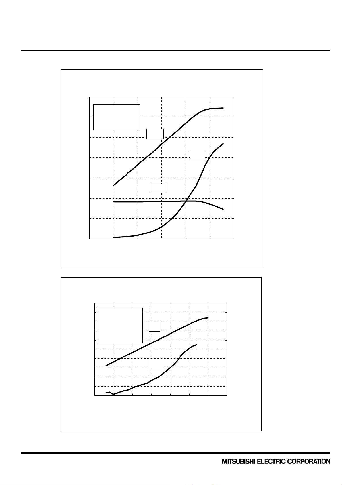
MGF09120A TYPICAL CHARACTERISTICS
Po,Gp ,PAE vs.P i
35
Vds=10V
Id(off)=400mA
30
f=1.9GHz
25
20
Po(dBm)
15
10
5
0
-10 -5 0 5 10 15 20
Po
PAE
Gp
Pin (dBm)
70
60
50
40
30
Gp(dB),PAE(%)
20
10
0
40
35
30
25
VD=10V
ID=400mA
f1=1.90GHz
f2=1.91GHz
20
15
10
5
Po(SCL)(dBm)
0
-5
-10
-15 -10 -5 0 5 10 15 20
Pi(SCL) vs. Po(SCL ) , IM3
Po
IM3
Pin(SCL)(dBm)
30
20
10
0
-10
-20
-30
-40
-50
-60
-70
IM3(dBc)
Publication Date : Apr., 2011
2
Page 3

< High-power GaAs FET (small signal gain stage) >
MGF0920A
L & S BAND / 1.6W
SMD non - matched
MGF0920A S PARAMETERS (Ta=25C,VD=10V,ID=400mA, Reference Plane see Fig.1)
freq. K MAG/MSG
(MHz) (mag) (ang) (mag) (ang) (mag) (ang) (mag) (ang) (dB)
600 0.930 -96.03 7.784 119.71 0.019 39.54 0.367 -155.36 0.25 26.12
1000 0.912 -124.52 5.692 100.24 0.023 26.68 0.427 -155.22 0.32 23.94
1400 0.903 -140.36 4.233 85.39 0.024 17.80 0.476 -154.99 0.42 22.46
1800 0.899 -149.63 3.242 73.85 0.024 12.03 0.516 -154.82 0.54 21.31
2200 0.899 -155.96 2.584 64.56 0.022 8.64 0.552 -154.81 0.75 20.70
2600 0.900 -161.19 2.156 56.76 0.021 7.04 0.583 -155.02 0.91 20.11
3000 0.901 -165.84 1.879 49.88 0.020 6.70 0.612 -155.50 1.06 18.23
3400 0.901 -169.78 1.696 43.51 0.019 7.24 0.638 -156.24 1.20 16.82
3800 0.900 -172.74 1.565 37.40 0.019 8.31 0.662 -157.24 1.24 16.23
4200 0.897 -174.91 1.462 31.40 0.020 9.66 0.684 -158.46 1.20 15.95
4600 0.893 -177.52 1.370 25.42 0.021 11.07 0.703 -159.84 1.19 15.54
5000 0.887 178.90 1.283 19.44 0.023 12.38 0.718 -161.35 1.15 15.13
5400 0.880 176.64 1.199 13.46 0.025 13.47 0.730 -162.91 1.15 14.48
5800 0.871 172.31 1.121 7.49 0.028 14.22 0.738 -164.48 1.14 13.73
6200 0.861 167.25 1.054 1.52 0.031 14.56 0.742 -166.00 1.18 12.76
6600 0.849 162.24 1.003 -4.44 0.034 14.40 0.744 -167.44 1.24 11.78
7000 0.836 157.65 0.971 -10.45 0.039 13.69 0.743 -168.79 1.20 11.27
7400 0.822 153.50 0.963 -16.57 0.044 12.36 0.739 -170.03 1.16 10.94
7800 0.805 149.52 0.978 -22.92 0.050 10.31 0.734 -171.21 1.10 10.98
8200 0.785 145.30 1.016 -29.63 0.058 7.49 0.728 -172.37 0.99 12.43
8600 0.761 140.29 1.071 -36.87 0.067 3.78 0.720 -173.62 0.90 12.04
9000 0.730 133.94 1.139 -44.85 0.078 -0.92 0.712 -175.10 0.82 11.64
9400 0.690 125.77 1.212 -53.74 0.093 -6.73 0.703 -176.99 0.75 11.15
9800 0.638 115.44 1.282 -63.76 0.110 -13.79 0.690 -179.52 0.74 10.66
10200 0.588 102.87 1.344 -75.07 0.131 -22.25 0.671 176.62 0.73 10.11
10600 0.547 88.25 1.393 -87.81 0.156 -32.28 0.644 172.09 0.72 9.51
11000 0.534 72.23 1.431 -102.03 0.186 -44.04 0.601 167.44 0.70 8.86
11400 0.562 55.90 1.464 -117.69 0.221 -57.73 0.537 162.49 0.66 8.21
11800 0.641 40.93 1.509 -134.63 0.260 -73.53 0.440 158.74 0.61 7.64
12200 0.770 29.66 1.597 -152.53 0.305 -91.61 0.300 165.54 0.58 7.19
Gate Mark
Round corner
S11 S21 S12 S22
2.0
0.8
(1)
(1)
0.80
Gate Mark
(2)
4.00
0.3
Fig. 1 O UTLIN E DRAW IN G
Publication Date : Apr., 2011
Reference Plane
4.20
0.25
(1) Gate
(3)
(2)
0.6
2.5
BACK SIDE PATTERN
Reference Plane
2.8
1.20
(2) Drain
(3) Source
(Unit:mm)
3
Page 4

< High-power GaAs FET (small signal gain stage) >
MGF0920A
L & S BAND / 1.6W
SMD non - matched
Mitsubishi Electric Corporation puts the maximum effort into making semiconductor product s better and more
reliable, but there is always the possibility that trouble may occur with them. Trouble with semiconductors
may lead to personal injury, fire or property damage. Remember to give due consideration to safety when
making your circuit designs, with appropriate measures such as (i) placement of substitutive, auxiliary
circuits, (ii) use of non-flammable material or (iii) prevention against any malfunction or mishap.
Keep safety first in your circuit designs!
•These materials are intended as a reference to assist our customers in the selection of the Mitsubishi
semiconductor product best suited to the customer’s application; they do not convey any license under any
intellectual property rights, or any other rights, belonging to Mitsubishi Electric Corporation or a third party.
•Mitsubishi Electric Corporation assumes no responsibility for any damage, or infringement of any
third-party’s rights, originating in the use of any product data, diagrams, charts, programs, algorithms, or
circuit application examples contained in these materials.
•All information contained in these materials, including product data, diagrams, charts, programs and
algorithms represents information on products at the time of publication of these materials, and are subject
to change by Mitsubishi Electric Corporation without notice due to product improvements or other reasons. It
is therefore recommended that customers contact Mitsubishi Electric Corporation or an authorized
Mitsubishi Semiconductor product distributor for the latest product information before purchasing a product
listed herein.
The information described here may contain technical inaccuracies or typographical errors. Mitsubishi
Electric Corporation assumes no responsibility for any damage, liability, or other loss rising from these
inaccuracies or errors.
Please also pay attention to information published by Mitsubishi Electric Corporation by various means,
including the Mitsubishi Semiconductor home page (http://www.MitsubishiElectric.com/).
•When using any or all of the information contained in these materials, including product data, diagrams,
charts, programs, and algorithms, please be sure to evaluate all information as a total system before making
a final decision on the applicability of the information and products. Mitsubishi Electric Corporation assumes
no responsibility for any damage, liability or other loss resulting from the information contained herein.
•Mitsubishi Electric Corporation semiconductors are not designed or manufactured for use in a device or
system that is used under circumstances in which human life is potentially at stake. Please contact
Mitsubishi Electric Corporation or an authorized Mitsubishi Semiconductor product distributor when
considering the use of a product contained herein for any specific purposes, such as apparatus or systems
for transportation, vehicular, medical, aerospace, nuclear, or undersea repeater use.
•The prior written approval of Mitsubishi Electric Corporation is necessary to reprint or reproduce in whole or
in part these materials.
•If these products or technologies are subject to the Japanese export control restrictions, they must be
exported under a license from the Japanese government and cannot be imported into a country other than
the approved destination.
Any diversion or re-export contrary to the export control laws and regulations of Japan and/or the country of
destination is prohibited.
•Please contact Mitsubishi Electric Corporation or an authorized Mitsubishi Semiconductor product distributor
for further details on these materials or the products contained therein.
Notes regarding these materials
© 2011 MITSUBISHI ELECTRIC CORPORATION. ALL RIGHTS RESERVED.
Publication Date : Apr., 2011
4
 Loading...