

Page 1
查询MGF0919A供应商
L & S BAND GaAs FET [ SMD non – matched ]
DESCRIPTION
The MGF0919A GaAs FET with an N-channel schottky
Gate, is designed for use UHF band amplifiers.
FEATURES
• High output power
Po=30dBm(TYP.) @f=1.9GHz,Pin=12dBm
• High power gain
Gp=19dB(TYP.) @f=1.9GHz
• High power added efficiency
ηadd=37%(TYP.) @f=1.9GHz,Pin=12dBm
• Hermetic Package
APPLICATION
• For UHF Band power amplifiers
QUALITY
• GG
RECOMMENDED BIAS CONDITIONS
• Vds=10V • Ids=300mA • Rg=500Ω
Delivery -01: Tape & Reel(1K), -03:Trai(50pcs)
Absolute maximum ratings (Ta=25°C)
Symbol
VGSO
VGDO
ID Drain current 800 mA
IGR Reverse gate current -2.4 mA
IGF Forward gate current 10 mA
PT Total power dissipation 6 W
Tch Cannel temperature 175 °C
Tstg Storage temperature -65 to +175 °C
Gate to source
Gate to drain breakdown voltage -15 V
Parameter Ratings Unit
breakdown voltage -15 V
MITSUBISHI SEMICONDUCTOR<GaAs FET>
MGF0919A
Fig.1
Electrical characteristics
Symbol
IDSS
VGS(off)
gm
Transconductance VDS=3V,ID=300mA - 260 - mS
Po Output power VDS=10V,ID=300mA,f=1.9GHz 28 30 - dBm
ηadd Power added Efficiency Pin=12dBm - 37 - %
GLP Linear Power Gain VDS=10V,ID=300mA,f=1.9GHz 17 19 - dB
NF Noise figure - 1.2 - dB
Rth(ch-c)
Min. Typ. Max.
Saturated drain current VDS=3V,V GS=0V - 600 800 mA
Gate to source cut-off voltage VDS=3V,ID=2.0mA -1.0 - -5.0 V
Thermal Resistance *1 ∆Vf Method - 17 25 °C/W
Parameter Test conditions Limits Unit
(Ta=25°C)
*1:Channel to case / Above parameters, ratings, limits are subject to change.
Mitsubishi Electric June/2004
Page 2
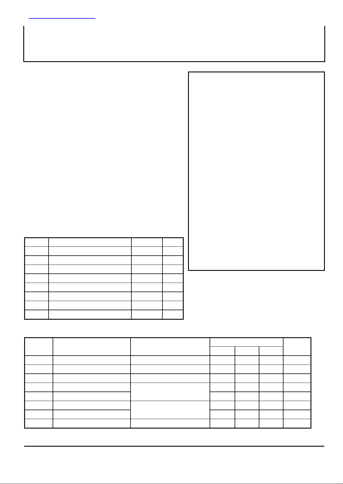
MGF0919A TYPICAL CHARACTERISTICS
VD=10V
Po,Gp,PAE vs.Pin
35
Vds=10V
Id(off)=300mA
f=1.9GHz
30
25
20
Po(dBm)
15
10
5
0
-10 -5 0 5 10 15
Po
PAE
Gp
70
60
50
40
30
Gp(dBm)PAE(%)
20
10
0
Pin(dBm)
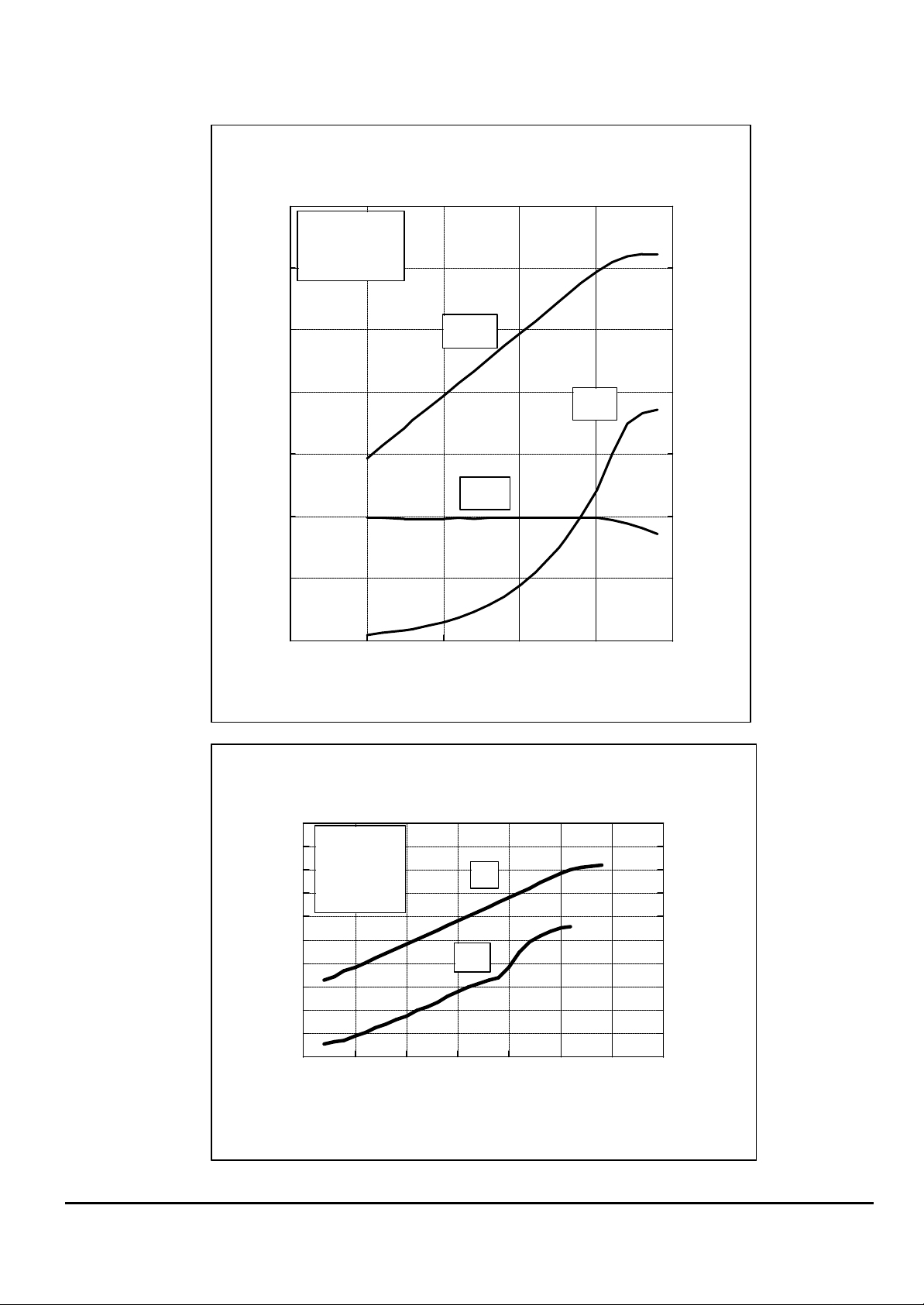
Pi(SCL) vs.Po(SCL),IM3
40
35
ID=300mA
30
25
f1=1.90GHz
f2=1.91Ghz
Po
20
15
10
5
Po(SCL)(dBm)
IM3
0
-5
-10
-15 -10 -5 0 5 10 15 20
Pin(SCL)(dBm)
30
20
10
0
-10
-20
-30
-40
-50
-60
-70
IM3(dBc)
Mitsubishi Electric June/2004
Page 3

MGF0919A S PARAMETERS
freq.
K
MAG/MSG
(MHz)
(mag)
(ang)
(mag)
(ang)
(mag)
(ang)
(mag)
(ang)
(dB)
600
0.933
-74.30
7.339
130.03
0.021
47.28
0.269
-137.41
0.25
25.43
1000
0.904
-103.32
5.703
108.92
0.029
31.40
0.341
-141.53
0.29
22.94
1400
0.888
-122.18
4.487
92.96
0.032
19.66
0.405
-144.12
0.35
21.47
1800
0.879
-134.53
3.597
80.59
0.032
10.98
0.460
-145.74
0.44
20.51
2200
0.876
-142.94
2.956
70.65
0.031
4.55
0.507
-146.82
0.55
19.79
2600
0.876
-149.11
2.499
62.27
0.029
-0.27
0.546
-147.71
0.68
19.35
3000
0.876
-154.07
2.175
54.80
0.028
-3.93
0.579
-148.61
0.80
18.90
3400
0.877
-158.32
1.946
47.84
0.027
-6.75
0.605
-149.68
0.90
18.58
3800
0.876
-162.04
1.780
41.10
0.027
-8.96
0.627
-151.00
0.96
18.19
4200
0.873
-165.28
1.655
34.44
0.028
-10.73
0.645
-152.57
0.99
17.72
4600
0.868
-168.13
1.557
27.78
0.029
-12.16
0.660
-154.36
1.03
16.20
5000
0.861
-170.89
1.475
21.10
0.030
-13.32
0.672
-156.31
1.10
14.98
5400
0.853
-174.26
1.405
14.42
0.032
-14.29
0.683
-158.32
1.12
14.31
5800
0.842
-179.57
1.345
7.74
0.034
-15.15
0.693
-160.29
1.16
13.55
6200
0.830
176.81
1.295
1.06
0.036
-15.98
0.701
-162.12
1.21
12.76
6600
0.818
170.87
1.257
-5.66
0.038
-16.89
0.708
-163.74
1.25
12.20
7000
0.803
163.91
1.235
-12.47
0.041
-18.03
0.712
-165.09
1.26
11.74
7400
0.788
157.93
1.229
-19.50
0.044
-19.57
0.713
-166.15
1.27
11.35
7800
0.772
153.18
1.244
-26.89
0.049
-21.70
0.711
-166.96
1.22
11.23
8200
0.753
148.85
1.279
-34.84
0.055
-24.65
0.703
-167.62
1.19
11.02
8600
0.732
143.64
1.334
-43.57
0.062
-28.65
0.690
-168.31
1.17
10.83
9000
0.706
136.22
1.405
-53.33
0.072
-33.94
0.670
-169.31
1.14
10.63
9400
0.667
125.58
1.487
-64.35
0.084
-40.75
0.643
-170.99
1.15
10.14
9800
0.623
111.25
1.574
-76.85
0.099
-49.26
0.608
-173.83
1.15
9.69
10200
0.590
93.44
1.653
-91.04
0.115
-59.62
0.566
-178.45
1.12
9.45
10600
0.584
73.04
1.713
-106.99
0.134
-71.91
0.517
177.11
1.06
9.59
11000
0.619
51.50
1.739
-124.73
0.152
-86.08
0.462
175.48
0.99
10.58
11400
0.696
30.59
1.712
-144.10
0.170
-101.97
0.391
-179.26
0.93
10.03
11800
0.800
12.12
1.612
-164.77
0.185
-119.23
0.384
-163.79
0.87
9.40
12200
0.899
-2.56
1.419
175.59
0.193
-137.32
0.463
-150.25
0.82
8.66
S11
S21
S12
S22
(Ta=25°C,VD=10V,ID=300mA, Reference Plane see Fig.1)
Gate Mark
Round corner
(1)
(2)
4.00
0.80
Gate Mark
(3)
BACK SIDE PATTERN
0.3
4.20
0.25
(1) Gate
(2) Drain
(3) Source
Fig.1 OUTLINE DRAWING
(Unit:mm)
2.0
0.8
2.5
(1)
(2)
0.6
Reference Plane
2.8
1.20
Reference Plane
Mitsubishi Electric June/2004
Page 4

MITSUBISHI SEMICONDUCTOR<GaAs FET>
MGF0919A
L & S BAND GaAs FET [ SMD non – matched ]
Requests Regarding Safety Designs
Mitsubishi Electric constantly strives to raise the level of its quality and reliability. Despite these concerted efforts,
however, there will be occasions when our semiconductor products suffer breakdowns, malfunctions or other
problems. In view of this reality, it is requested that every feasible precaution be taken in the pursuit of redundancy
design, malfunction prevention design and other safety -related designs, to prevent breakdowns or malfunctions in our
products from resulting in accidents involving people, fires, social losses or other problems, thereby upholding the
highest levels of safety in the products when in use by customers.
Matters of Importance when Using these Materials
1. These materials are designed as reference materials to ensure that all customers purchase Mitsubishi Electric
semiconductors best suited to their specific use applications. Please be aware, however, that the technical
information contained in these materials does not comprise consent for the execution or use of intellectual property
rights or other rights owned by Mitsubishi Electric Corporation.
2. Mitsubishi Electric does not assume responsibility for damages resulting from the use of product data, graphs,
charts, programs, algorithms or other applied circuit examples described in these materials, or for the infringement
of the rights of third-party owners resulting from such use.
3. The data, graphs, charts, programs, algorithms and all other information described in thes e materials were current
at the issue of these materials, with Mitsubishi Electric reserving the right to make any necessary updates or
changes in the products or specifications in these materials without prior notice. Before purchasing Mitsubishi
Electric semiconductor products, therefore, please obtain the latest available information from Mitsubishi Electric
directly or an authorized dealer.
4. Every possible effort has been made to ensure that the information described in these materials is fully accurate.
However, Mitsubishi Electric assumes no responsibility for damages resulting from inaccuracies occurring within
these materials.
5. When using the product data, technical contents indicated on the graphs, charts, programs or algorithms described
in these materials, assessments should not be limited to only the technical contents, programs and algorithm units.
Rather, it is requested that ample evaluations be made of each individual system as a whole, with the customer
assuming full responsibility for decisions on the propriety of application. Mitsubishi Electric does not accept
responsibility for the propriety of application.
6. The products described in these materials, with the exception of special mention concerning use and reliability, have
been designed and manufactured with the purpose of use in general electronic machinery. Accordingly these
products have not been designed and manufactured with the purpose of application in machinery or systems that will
be used under conditions that can affect hum an life, or in machinery or systems used in social infrastructure that
demand a particularly high degree of reliability. When considering the use of the products described in these
materials in transportation machinery (automobiles, trains, vessels), for objectives related to medical treatment,
aerospace, nuclear power control, submarine repeaters or systems or other specialized applications, please consult
with Mitsubishi Electric directly or an authorized dealer.
7. When considering use of products for purposes other than the specific applications described in these materials,
please inquire at Mitsubishi Electric or an authorized dealer.
8. The prior consent of Mitsubishi Electric in writing is required for any reprinting or reproduction of these materials.
9. Please direct any inquiries regarding further details of these materials, or any other comments or matters of attention,
to Mitsubishi Electric or an authorized dealer.
Mitsubishi Electric June/2004
 Loading...