Mitsubishi MF38M1-LSDAGXX, MF38M1-LCDAGXX Datasheet

MITSUBISHI MEMORY CARD
STATIC RAM CARDS
8/16-bit Data Bus
Static RAM Card
Connector Type
Two- piece 68-pin
DESCRIPTION
Mitsubishi’s Static RAM cards provide large
memory capacities on a device approximately the
size of a credit card(85.6mm×54mm×5.0mm).
The cards use an 8/16 bit data bus.The devices
use a replaceable lithium battery to maintain
data.Available in 8Mbyte capacities,
Mitsubishi’s Static RAM cards are available
with a 68-pin, two-piece connector.
FEATURES
nUses TSOP (Thin Small Outline Package) to
achieve very high memory density coupled
with high reliability, without enlarging card
size.
MF38M1-LCDAGXX
MF38M1-LSDAGXX
nElectrostatic discharge protection to 15kV
nBuffered interface
n68pin connector
n8-bit and 16-bit data width
nWrite protect switch
nBattery voltage pin
nLS Type Wide Range operating temperature
(Ta= -20 to 70°C)
APPLICATIONS
nOffice automation nIndustrial
nData Communication nTelecommunications
nComputers nConsumer
PRODUCT LIST
Item Memory Data Bus Attribute Auxialiary Memory Outline Main battery
Type name capacity width(bits) memory battery organization drawing holder
MF38M1-LCDAGXX 8MB 8/16 NO NO 4M bit SRAM×16 68P-010 Screw type
MF38M1-LSDAGXX 8MB 8/16 NO NO 4M bit SRAM×16 68P-010 Screw type
MITSUBISHI
ELECTRIC
1/9

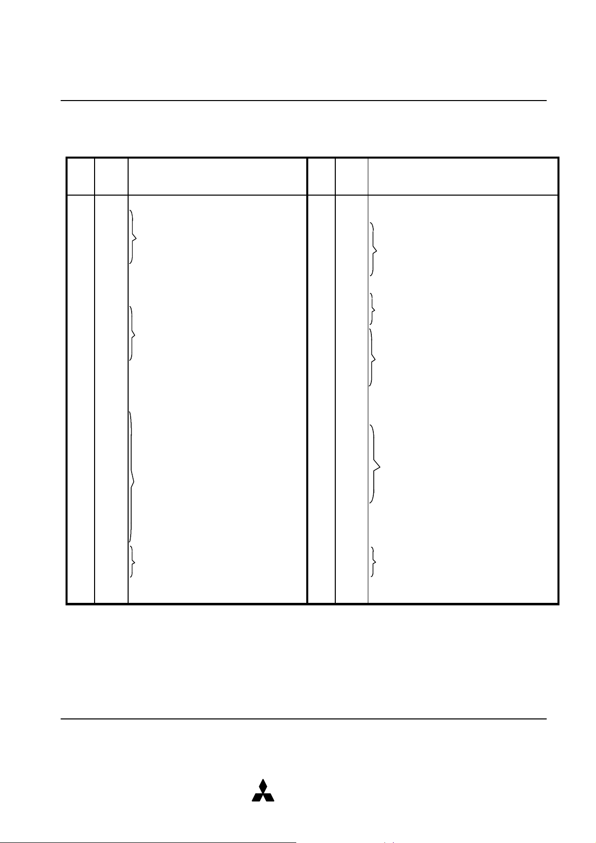
PIN ASSIGNMENT
1
GND
Ground
35
GND
Ground
2
D3
36
CD1#
Card detect 1
3
D4
37
D11
4D5 Data I/O
38
D12
5
D6
39
D13
Data I/O
6
D7
40
D14
7
CE1#
Card enable 1
41
D15
8
A10
Address input
42
CE2#
Card enable 2
9
OE#
Output enable
43
NC
10
A11
44NC No connection
11
A9
45
NC
12A8 Address input
46
A17
13
A13
47
A18
14
A14
48
A19
Address input
15
WE#
Write enable
49
A20
16NCNo connection
50
A21
17
VCCPower supply voltage
51
VCC Power supply voltage
18NCNo connection
52NCNo connection
19
A16
53
A22
Address input
20
A15
54
NC
21
A12
55
NC
22
A7
56
NC
23
A6
57NC No connection
24A5 Address input
58
NC
25
A4
59
NC
26
A3
60
NC
27
A2
61
REG#
REG function
28
A1
62
BVD2
Battery voltage detect 2
29
A0
63
BVD1
Battery voltage detect 1
30
D0
64
D8
31D1 Data I/O
65D9 Data I/O
32
D2
66
D10
33WPWrite protect
67
CD2#
Card detect 2
34
GND
Ground
68
GND
Ground
Two-Piece Type (68-pin)
MITSUBISHI MEMORY CARD
STATIC RAM CARDS
Pin Pin
Symbol
No. No.
Function
Symbol
Function
WRITE PROTECT MODE (WP)
When the write protect switch is switched on, this
card goes into a write protect mode that can read
but not write data.
In this mode, WP pin becomes “H” level.
At the shipment the write protect switch is switched
off (Normal mode : The card can be written ; WP pin
indicates “L” level).
MITSUBISHI
ELECTRIC
2/9

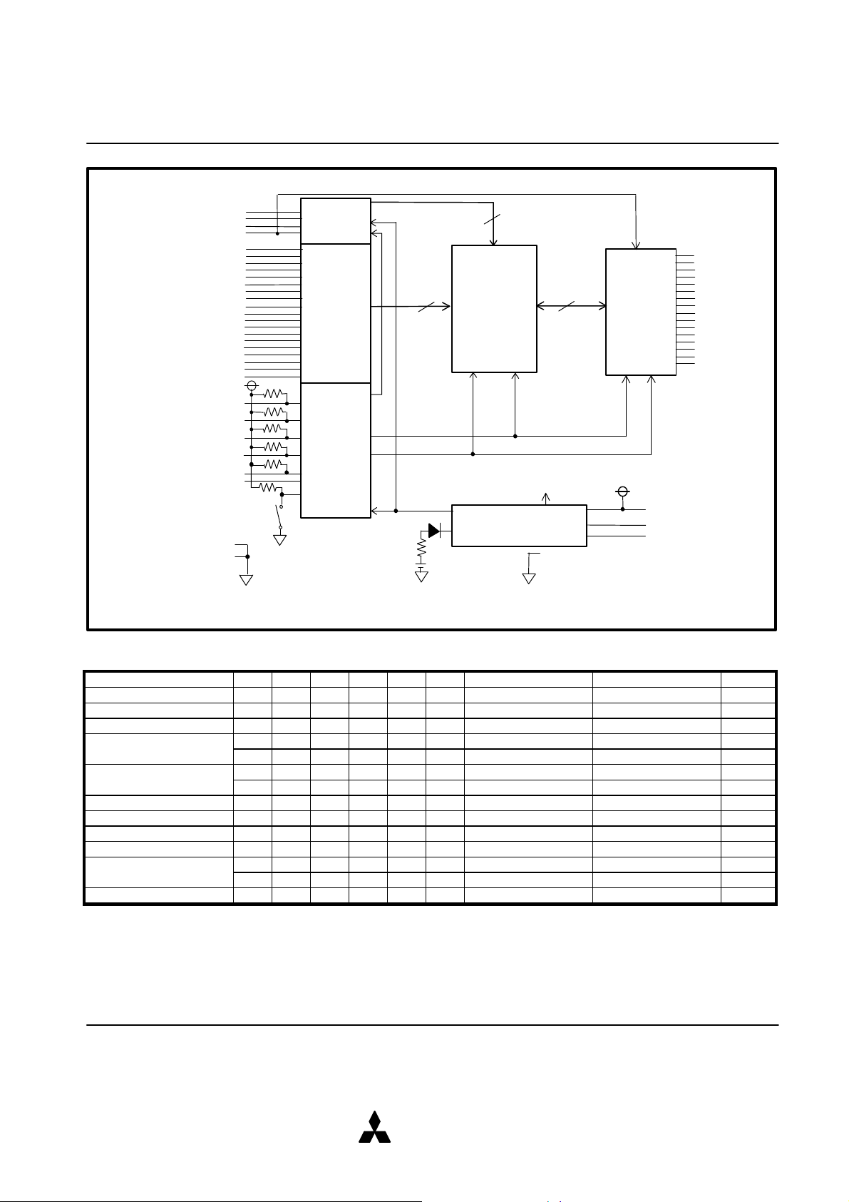
BLOCK DIAGRAM (8MB)
A22
D15
BVD2
WP#
WRITE ROTECT
ON
OFF
19
16
BR2325
POWER CONTROLLER
16
MITSUBISHI MEMORY CARD
STATIC RAM CARDS
CE1#
CE2#
WE#
OE#
REG#
CD1#
CD2#
A21
A20
A0
A19
A18
A17
A16
A15
A14
A13
A12
A11
A10
A9
A8
A7
A6
A5
A4
A3
A2
A1
ADDRESSDECODER
ADDRESS-
BUS
BUFFERS
MODE
CONTROL
LOGIC
CS#
COMMON
MEMORY
4Mbit SRAM×16
OE# WE#
TO INTERNAL
POWER SUPPLY
VOLTAGE DETECTOR
&
GND
DATA-BUS
BUFFERS
VCC
BVD1
D14
D13
D12
D11
D10
D9
D8
D7
D6
D5
D4
D3
D2
D1
D0
FUNCTION TABLE
Mode
REG# CE1# CE2# OE# WE# A0
Standby X H H X X X High-impedance High-impedance Standby
Read A (16bit) common H L L L H X Odd Byte Data out Even Byte Data out Active
Write A (16bit) common H L L H L X Odd Byte Data in Even Byte Data in Active
Read B (8bit) common H L H L H L High-impedance Even Byte Data out Active
H L H L H H High-impedance Odd Byte Data out Active
Write B (8bit) common H L H H L L High-impedance Even Byte Data in Active
H L H H L H High-impedance Odd Byte Data in Active
Read C (8bit) common H H L L H X Odd Byte Data out High-impedance Active
Write C (8bit) common H H L H L X Odd Byte Data in High-impedance Active
Output disable X X X H H X High-impedance High-impedance Active
Read A (16bit) attribute L L L L H X Data out (unknown) Data out (FFh) Active
Read B (8bit) attribute L L H L H L High-impedance Data out (FFh) Active
L L H L H H High-impedance Data out (unknown) Active
Read C (8bit) attribute L H L L H X Data out (unknown) High-impedance Active
I/O (D15~D8) I/O (D7~D0) ICC
Note 1 : H=VIH, L=VIL, X=VIH or VIL
MITSUBISHI
ELECTRIC
3/9
 Loading...