Mitsubishi MF365A-LZCATXX, MF3257-LZCATXX, MF34M1-LZCATXX, MF3129-LZCATXX, MF32M1-LZCATXX Datasheet
...
MITSUBISHI MEMORY CARD
STATIC RAM CARDS
8/16-bit Data Bus
Static RAM Card
Connector Type
Two- piece 68-pin
1. DESCRIPTION
Mitsubishi’s Static RAM cards provide large memory
capacities on a device approximately the size of a
credit card (85.6mm×54mm×3.3mm).
The cards use a 8/16 bit data-bus. The devices use a
replaceable lithium battery to maintain data.
Available in 64K byte-4M byte capacities,
Mitsubishi’s Static RAM cards are available with a
68-pin, two-piece connector.
MF365A-LZCATXX
MF3129-LZCATXX
MF3257-LZCATXX
MF3513-LZCATXX
MF31M1-LZCATXX
MF32M1-LZCATXX
MF34M1-LZCATXX
2. FEATURES
nUses TSOP (Thin Small Outline Package) to
achieve very high memory density coupled with
high reliability, without enlarging card size
nElectrostatic discharge protection to 15kV
nBuffered interface
nWrite protect switch
nAttribute memory
n68pin
3. APPLICATIONS
nOffice automation nData Communication
nComputers nIndustrial
nTelecommunications nConsumer
4. PRODUCT LIST
Item Memory Data Bus Attribute Auxiliary
Type name capacity width(bits) memory battery
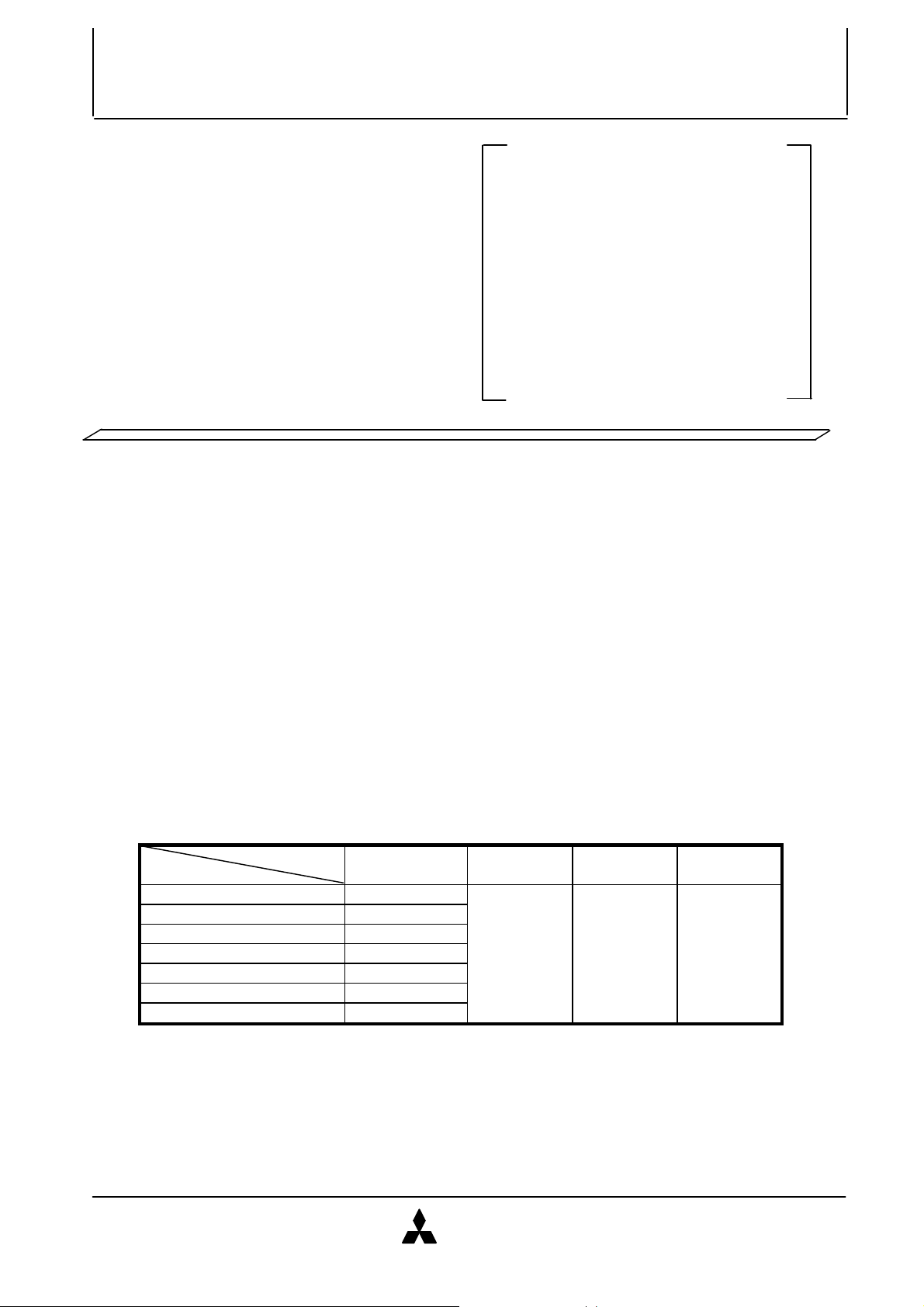
MF365A-LZCATXX 64KB
MF3129-LZCATXX 128KB
MF3257-LZCATXX 256KB
MF3513-LZCATXX 512KB 8/16 8KB NO
MF31M1-LZCATXX 1MB E2PROM
MF32M1-LZCATXX 2MB
MF34M1-LZCATXX 4MB
MITSUBISHI
ELECTRIC
1/16 Apr. 1999 Rev. 1.1

MITSUBISHI MEMORY CARD
STATIC RAM CARDS
5. SUMMARY
MF3XXX-LZCATXX series is the Static RAM cards which has 8/16 bit changeable data-bus width.
The card has a replaceable lithium battery to maintain data in memory. When the card is not use or the supply
voltage drops, the battery will automatically maintain data in memory.
6. FUNCTIONAL DESCRIPTION
The function of the card is determined by the combination of the following five control signals,
REG#, CE1#, CE2#, OE#, WE#; active low signals. (Please refer to section 10 FUNCTION TABLE on page 5)
((1))COMMON MEMORY FUNCTION
When REG# signal is high level, the common memory area is selected.
((a))READ MODE
To read, WE# is set high level and CE1# or CE2# is set low level and the memory address is applied at inputs
A0-A21(4MB). Setting OE# low level executes the reading with output at data-bus. It is available to make the
following functions according to the combination of CE1# and CE2#.
When CE1# is set low level and CE2# is set high level, the card operates as an 8 bit data-bus width card.
The data can be dealt with lower data-bus(D0-D7).
When both CE1# and CE2# are set low level, the card operates as a 16 bit data-bus width card.
At this mode LSB of address-bus (A0) is ignored.
In addition odd byte can be accessed through upper data-bus(D8-D15) when CE1# is set high level and CE2# is
set low level. This mode is useful when handling only odd bytes in the 16 bit data-bus interface system (A0 is
ignored).
When both CE1# and CE2# are set high level, the card becomes a standby mode where the card consumes
low power and the data-bus is placed in high impedance state (above functions of CE1# and CE2# are the same
as in the following modes).
When both OE# and WE# are set high level, the card becomes a output disable mode and the data-bus is
placed in high impedance state.
((b))WRITE MODE
To write, the memory address is first applied at inputs A0-A21(4MB) and the data is applied at output pins.
Setting CE1# or CE2# low level, WE# low level and OE# high level executes the writing.
((2))ATTRIBUTE MEMORY FUNCTION
When REG# is set low level, the attribute memory area is selected. MF3XXX-LZCATXX series accommodates
an attribute memory of 8KB E2PROM on even addresses.
((a))READ MODE
First set CE1# and CE2# low level or high level and select residing address (even address). Data can be read by
setting OE# low level and WE# high level.
((b))WRITE MODE
Writing can be done either by byte-mode or page-mode. The page-mode write is the function to be able to write
data of 32 bytes in a single write cycle. The page address is set by A6 to A13 (Please note that attribute memory
exists in even bytes only). To write, set OE# high level and WE# low level. Data will be latched at the rising
edge of WE#. After the first load unless WE# changes from high level to low level within 30µs, the automatic
erase/program starts and completes in 10ms or before. Page data can be latched if WE# transits from high level
to low level before the 30µs. Page-mode write also executes erase/program operation within 10ms.
The page address must be maintained during the page data loading.
7. WRITE PROTECT MODE
When the write protect switch is switched on, this card goes into a write protect mode that can read but not
write data. In this mode, WP pin becomes “H” level.
At the shipment the write protect switch is switched off (Normal mode : The card can be written ; WP pin
indicates “L” level).
MITSUBISHI
ELECTRIC
2/16 Apr. 1999 Rev. 1.1

MITSUBISHI MEMORY CARD
1
GND
Ground
35
GND
Ground
A17 (NC for < 128KB types)
A18 (NC for < 256KB types)
A19 (NC for < 512KB types) Address
A20 (NC for < 1MB type) input
A21 (NC for < 2MB type)
STATIC RAM CARDS
8. PIN ASSIGNMENTS
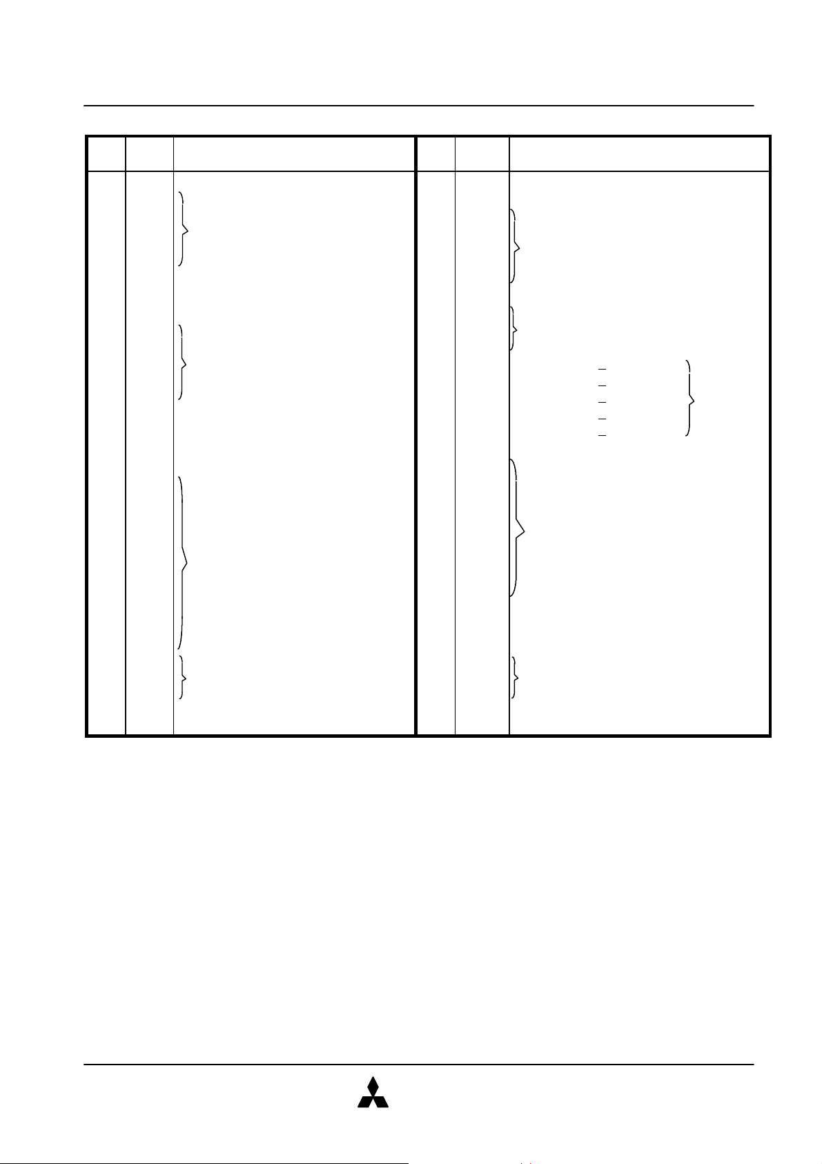
Pin Pin
Symbol
No. No.
Function
Symbol
Function
2 D3 36 CD1# Card detect 1
3 D4 37 D11
4 D5 Data I/O 38 D12
5 D6 39 D13 Data I/O
6 D7 40 D14
7 CE1# Card enable 1 41 D15
8 A10 Address input 42 CE2# Card enable 2
9 OE# Output enable 43 NC
10 A11 44 NC No connection
11 A9 45 NC
12 A8 Address input 46 A17
13 A13 47 A18
14 A14 48 A19
15 WE# Write enable 49 A20
16 NC No connection 50 A21
17 VCC Power supply voltage 51 VCC Power supply voltage
18 NC No connection 52 NC
19 A16 A16 (NC for 64KB type) 53 NC
20 A15 54 NC
21 A12 55 NC
22 A7 56 NC No connection
23 A6 57 NC
24 A5 Address input 58 NC
25 A4 59 NC
26 A3 60 NC
27 A2 61 REG# Attribute memory select
28 A1 62 BVD2 Battery voltage detect 2
29 A0 63 BVD1 Battery voltage detect 1
30 D0 64 D8
31 D1 Data I/O 65 D9 Data I/O
32 D2 66 D10
33 WP Write protect 67 CD2# Card detect 2
34 GND Ground 68 GND Ground
MITSUBISHI
ELECTRIC
3/16 Apr. 1999 Rev. 1.1

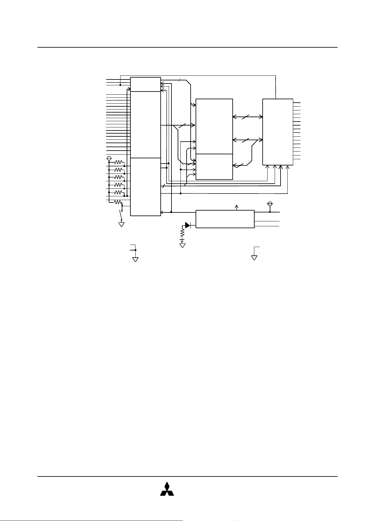
9. BLOCK DIAGRAM (4MB) (MF34M1-LZCATXX)
A21
WP#
WRITE PROTECT
ON
13
1988
POWER CONTROLLER
DECODER
8
CR2025
2
MITSUBISHI MEMORY CARD
STATIC RAM CARDS
CE1#
CE2#
WE#
OE#
REG#
A20
A0
A19
A18
A17
A16
A15
A14
A13
A12
A11
A10
A9
A8
A7
A6
A5
A4
A3
A2
A1
OFF
CD1#
CD2#
ADDRESS-
ADDRESS-
BUS
BUFFERS
MODE
CONTROL
LOGIC
9
D15
CS#
COMMON
MEMORY
4Mbit SRAM×8
OE#
WE#
CS#
ATTRIBUTE
MEMORY
OE#
64Kbit
E2PROM×1
WE#
TO INTERNAL
POWER SUPPLY
VOLTAGE DETECTOR
&
DATA-BUS
BUFFERS
VCC
BVD2
D14
D13
D12
D11
D10
D9
D8
D7
D6
D5
D4
D3
D2
D1
D0
BVD1
GND
MITSUBISHI
ELECTRIC
4/16 Apr. 1999 Rev. 1.1

MITSUBISHI MEMORY CARD
STATIC RAM CARDS
10. FUNCTION TABLE
Mode REG# CE1# CE2# OE# WE# A0 I/O (D15~D8) I/O (D7~D0) Icc
Standby X H H X X X High-impedance High-impedance standby
Read A (16bit)
common
Write A (16bit)
common
Read B (8bit)
common
H L L L H X Odd Byte
Data out
H L L H L X Odd Byte
Data in
Even Byte
Data out
Even Byte
Data in
H L H L H L High-impedance Even Byte
Data out
H L H L H H High-impedance Odd Byte
Active
Active
Active
Active
Data out
Write B (8bit)
H L H H L L High-impedance Even Byte Data in Active
common H L H H L H High-impedance Odd Byte Data in Active
Read C (8bit)
common
Write C (8bit)
common
H H L L H X Odd Byte
Data out
H H L H L X Odd Byte
Data in
High-impedance Active
High-impedance Active
Output disable X X X H H X High-impedance High-impedance Active
Read A (16bit)
attribute
Read B (8bit)
attribute
L L L L H X Data out
(unknown)
Even Byte
Data out
L L H L H L High-impedance Even Byte
Data out
L L H L H H High-impedance Data out
Active
Active
Active
(unknown)
Read C (8bit)
attribute
Write A (16bit)
L H L L H X Data out
High-impedance Active
(unknown)
L L L H L X don’t care Even Byte Data in Active
attribute
Write B (8bit)
L L H H L L don’t care Even Byte Data in Active
attribute L L H H L H don’t care don’t care Active
Write C (8bit)
L H L H L X don’t care don’t care Active
attribute
Note 1 : H=VIH, L=VIL, X=VIH or VIL
11. ABSOLUTE MAXIMUM RATINGS
Symbol Parameter Conditions Ratings Unit
Vcc Supply voltage -0.3~6.0 V
VI Input voltage With respect to GND -0.3~VCC+0.3 V
VO Output voltage 0~VCC V
Topr1 Operating temperature 1 Read, Write Operation 0~60 °C
Topr2 Operating temperature 2 Data retention 0~60 °C
Tstg Storage temperature Excludes data retention -20~70 °C
12. RECOMMENDED OPERATING CONDITIONS (Ta=0~55°C, unless otherwise noted)
Symbol
Parameter
Min. Typ. Max.
Limits
Unit
Vcc Vcc Supply voltage 4.75 5.0 5.25 V
GND System ground 0 V
VIH High input voltage 2.4 VCC V
VIL Low input voltage 0 0.8 V
MITSUBISHI
ELECTRIC
5/16 Apr. 1999 Rev. 1.1
 Loading...