

Mitsubishi MF-10KDS-R13-071, MF-10KDS-R13-060, MF-10KDS-R13-061, MF-10KDS-R13-070, MF-10KDS-12T-071 Datasheet
...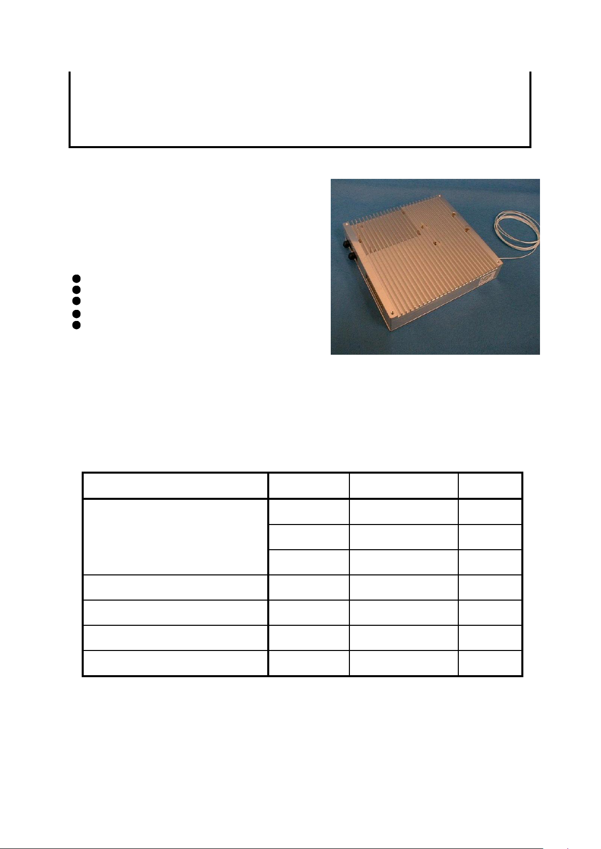
MITSUBISHI (OPTICAL DEVICES)
MF-10KDS-T12-06x/07x
MF-10KDS-R13-06x/07x
SONET/SDH TRANSMITTER & RECIEVER
DESCRIPTION
Th is prod uct is designed to provide high optic al
performance for SDH STM-64/SONE T OC-192.
Trans mitte r us es co oled laser in a but t erf ly pac kag e
module wit h driv ered by spec ific integrated circuit.
Receiver us es PD preamp -modul e (butterf ly package
module) and integrat ed circuit s for reshaping, retim ing
and regenerating optical signal.
FEATURES
Full SONET/SDH line up
K connector interface
-5.2V,+5V power supply target, -2.2V(TX only)
Case Temp. Range: 10 to 65°C
Clock recovery and digital alarm function.
APPLICATION
Short haul and long haul telecommunication systems
for SDH STM64 / SONET OC-192.
ABSOLUTE MAXIMUM RATINGS
Stress below listed absolute maximum rating may cause permanent damage to the transmitter and receiver.
This is a stress only and func tional operation of the transceiver at these or any other conditions in excess of those
given in the operational sections of this data sheet is not implied.
Exposure to Absolute Maximum Rating for extended periods may affect transmitter and receiver reliability.
Tc=25°C
Parameters Symbol Ratings Unit
Vcc +5.3 V
Vee -6.0 VSupply voltage
Vtt -2.4 V
Storage temperature Tstg -40 to 85
°
C
Operating case temperature Tc 10 to 65
°
C
Relative humidity(non condensation) - 10 to 80 %
Fiber bend radius rF 32 mm
MITSUBISHI (OPTICAL DEVICES)
MF-10KDS-T12-06x/07x
MF-10KDS-R13-06x/07x
SONET/SDH TRANSMITTER & RECIEVER
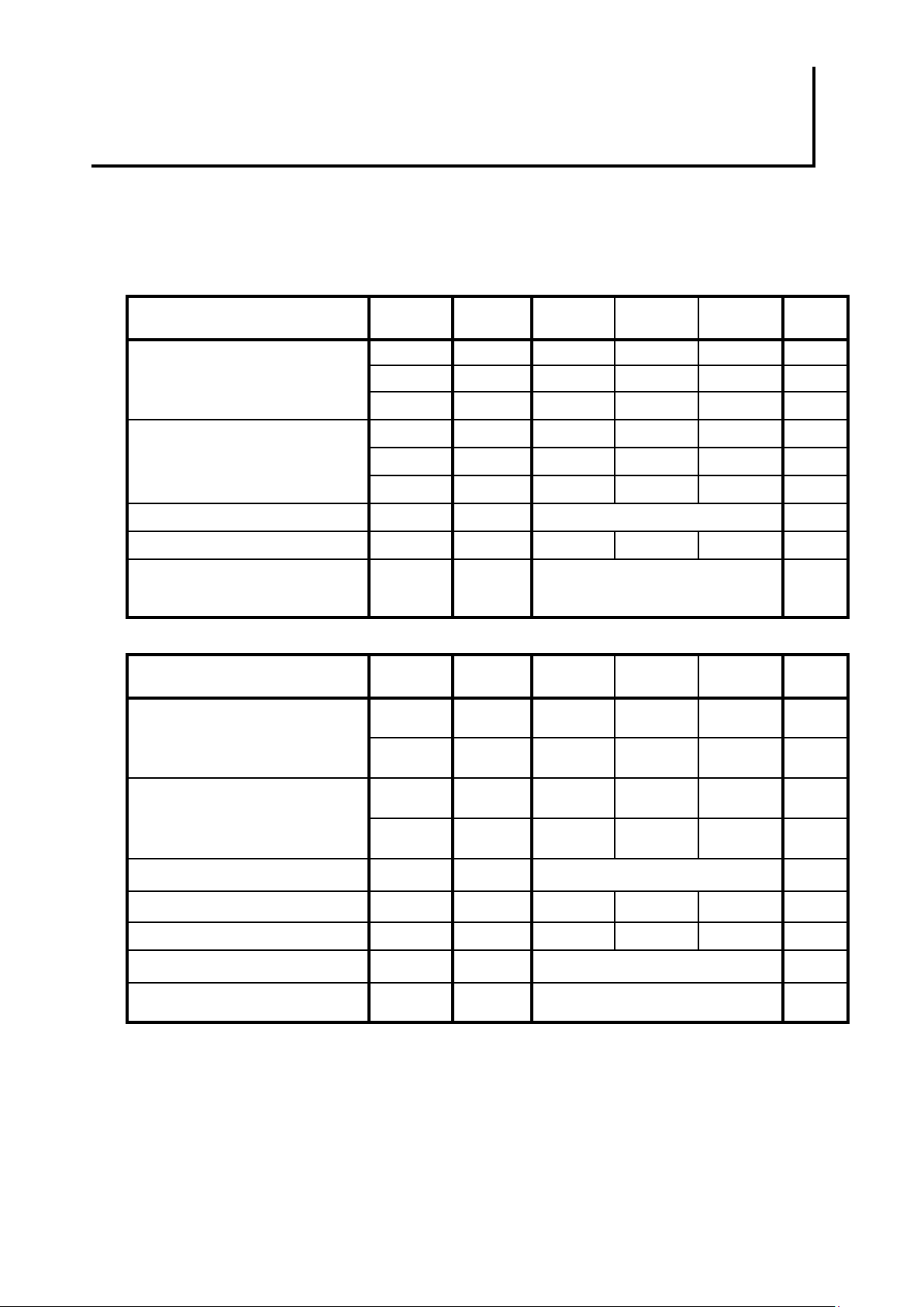
ELECTRICAL CHARACTERISTICS
All parameters are specified over the operating case temperature.
Measurement conditions are at 9953.28Mb/s+/-20ppm, NRZ PN2
23
-1 and 50%duty cycle data signal.
Vcc=+5.0V+/-5%, Vee=-5.2V+/-5%, Vtt=-2.2V+/-0.1V,Tc=10 to 65 °C, Using a PRBS 2
23
-1 pattern with a
50%Mark ratio, unless otherwise noted.
Transmitter
Parameters Condition Symbol Min. Typ. Max. Unit
Vee -5.46 -5.2 -4.94 V
Vcc 4.75 5.0 5.25 V
Supply voltage
Vtt -2.3 -2.2 -2.1 V
Iee - - 1.5 A
Icc - - 1.0 A
Supply current
Itt - -
1. 2
A
Data / Clock input voltage (DC:50ohm) note 1 - SCFL Data / Clock relationship note 5 Td -20 - +20 psec
Function note 2,3 -
Sh utdow n, Laser Degr adati on, Power out
of rang e Alarm, Laser Over Tem pera ture
Alarm
-
Receiver
Parameters Condition Symbol Min. Typ. Max. Unit
Vee -5.46 -5.2 -4.94 V
Supply voltage
Vcc 4.75 5.0 5.25 V
Iee - - 1.5 A
Supply current
Icc - - 1.5 A
Data output voltage (DC:50ohm) note 4 - SCFL -
Clock output voltage (AC:50ohm) note 4 0.5 - 1.5 Vpp
Data / Clock relationship note 5 Td -25 - +25 psec
Jitter - TBD -
Function note 6 - Loss of Signal Alarm -
MITSUBISHI (OPTICAL DEVICES)
MF-10KDS-T12-06x/07x
MF-10KDS-R13-06x/07x
SONET/SDH TRANSMITTER & RECIEVER
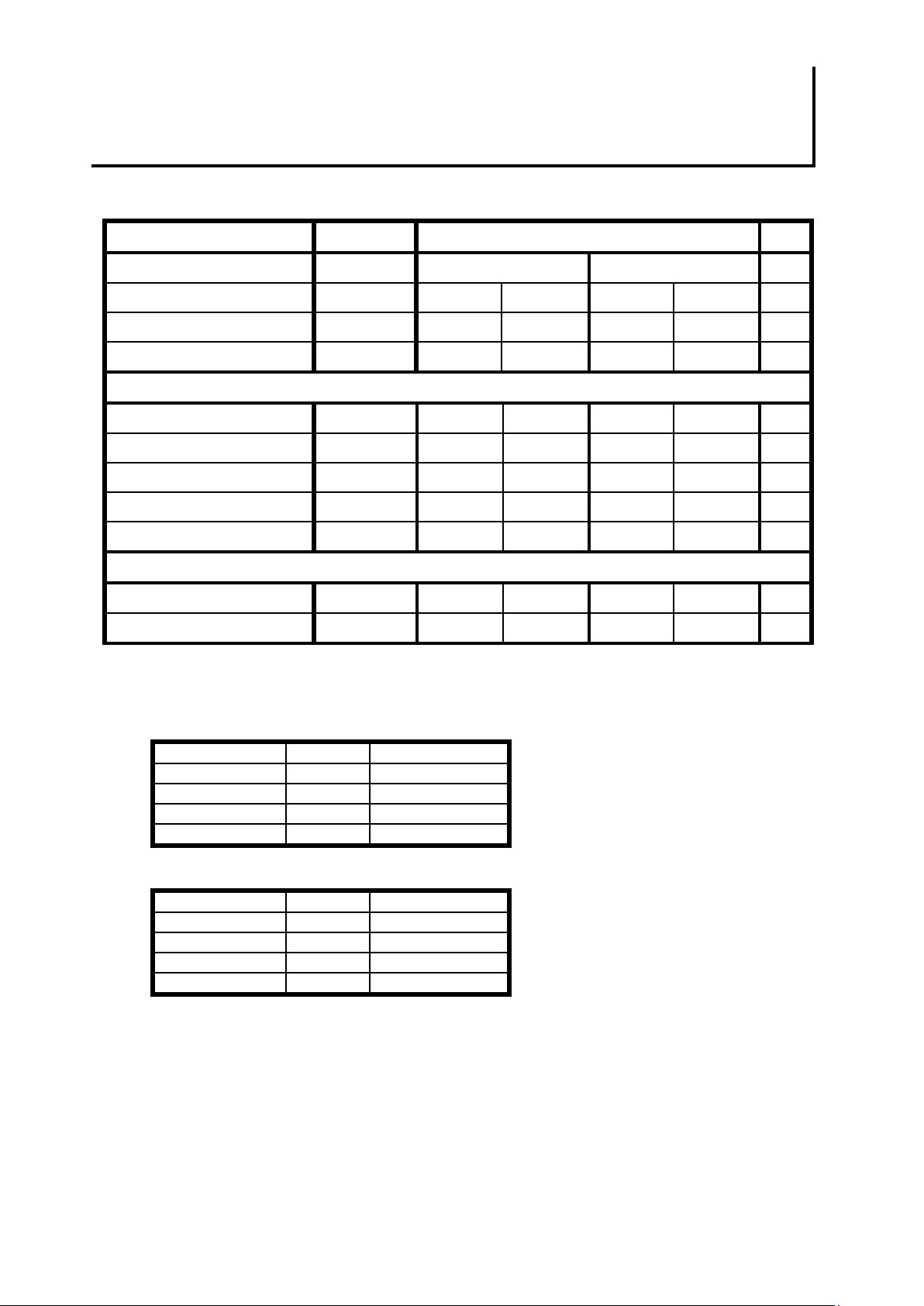
OPTICAL CHARACTERISTICS
Parameter Symbol Specification Unit
ITU code - S-64.2 S-64.3 -
- - Min. Max. Min. Max. Dispersion - -800 +800 -130 +130 ps/nm
Optical path penalty Pp - 2 - 1 dB
Transmitter
Wavelength - 1530 1565 1530 1565 Optical output power Pout -3 +3 -2 +3 dBm
Spectral width(-20dB) - - 0.5 - 0.5 nm
SMSR - 30 - 30 - dB
Extinction Ratio Ex 8.2 - 8.2 - dB
Receiver
Sensitivity - - -14 - -13 dBm
Overload - -3 - -3 - dBm
note : Bit Rate 9953.28Mb/s,PRBS223-1, BER<=10
-12
ORDERING INFORMATION
Transmitter
Part number ITU-code Optical connector type
MF-10KDS-T12-060 S-64.2 FC
MF-10KDS-T12-061 S-64.2 SC
MF-10KDS-T12-070 S-64.3 FC
MF-10KDS-T12-071 S-64.3 SC
Receiver
Part number ITU-code Optical connector type
MF-10KDS-R13-060 S-64.2 FC
MF-10KDS-R13-061 S-64.2 SC
MF-10KDS-R13-070 S-64.3 FC
MF-10KDS-R13-071 S-64.3 SC

MITSUBISHI (OPTICAL DEVICES)
MF-10KDS-T12-06x/07x
MF-10KDS-R13-06x/07x
SONET/SDH TRANSMITTER & RECIEVER
TRANSMITTER PIN ALLOCATION
No. Symbol Description No. Symbol Description
1 -2.2V Supply voltage for cooler 2 -2.2V Supply voltage for cooler
3 GND Ground 4 NUC No user connection
5 LDMON Laser Bias Monitor 6 PDMON Laser Backface Monitor
7 DEG Laser Degradation Alarm 8 ORA Power Out of Range Alarm
9 LOT Laser Over Temperature Alarm 10 SDC Shut Down Command
11 GND Ground 12 GND Ground
13 GND Ground 14 GND Ground
15 +5V Supply voltage 16 +5V Supply voltage
17 +5V Supply voltage 18 +5V Supply voltage
19 GND Ground 20 GND Ground
21 GND Ground 22 GND Ground
23 -5.2V Supply voltage 24 -5.2V Supply voltage
25 -5.2V Supply voltage 26 -5.2V Supply voltage
27 GND Ground 28 GND Ground
29 GND Ground 30 GND Ground
RECEIVER PIN ALLOCATION
No. Symbol Description No. Symbol Description
1 GND Ground 2 GND Ground
3 GND Ground 4 LOS Loss of signal alarm
5 NUC No user connection 6 NUC No user connection
7 NUC No user connection 8 NUC No user connection
9 NUC No user connection 10 NUC No user connection
11 GND Ground 12 GND Ground
13 GND Ground 14 GND Ground
15 +5V Supply voltage 16 +5V Supply voltage
17 +5V Supply voltage 18 +5V Supply voltage
19 GND Ground 20 GND Ground
21 GND Ground 22 GND Ground
23 -5.2V Supply voltage 24 -5.2V Supply voltage
25 -5.2V Supply voltage 26 -5.2V Supply voltage
27 GND Ground 28 GND Ground
29 GND Ground 30 GND Ground

MITSUBISHI (OPTICAL DEVICES)
MF-10KDS-T12-06x/07x
MF-10KDS-R13-06x/07x
SONET/SDH TRANSMITTER & RECIEVER
GENERAL OUTLINE DRAWING
NOTE: TOLERANCES UNLESS NOTED +/-0.5
DIMENSIONS ARE IN MILLIMETERS
Transmitter
Receiver

MITSUBISHI (OPTICAL DEVICES)
MF-10KDS-T12-06x/07x
MF-10KDS-R13-06x/07x
SONET/SDH TRANSMITTER & RECIEVER
BLOCK DIAGRAM
Alarm
PLL
DATAout
DATAout
CLKout
CLKout
LOS
OPT. IN
Receiver
Clock recovery IC
Preamp
PD-Preamp Module
PD
EA-LD Module
Driver IC
A.P.C
DATAin
DATAin
DRIVER IC
PD
LD
LOT
ORA
DEG
integrated device
OPT. OUT
Transmitter
VCC VCC
CLOCK
CLOCK
SDC
A.T.C
Cooler
Thermistor

MITSUBISHI (OPTICAL DEVICES)
MF-10KDS-T12-06x/07x
MF-10KDS-R13-06x/07x
SONET/SDH TRANSMITTER & RECIEVER
NOTE
NOTE1: Input interface
NOTE2: Shut down interface
NOTE3: Laser Degradation Alarm / Power out of range Alarm / LD temperature out of range Alarm
Laser Degradation Alarm (DEG ) set s when the bias current is at least 70% higher than
the maximum initial value allowed .
Alarm active: TTL LOW
Power out of range Alarm (OR A), sets when the output opt ical output pow er is 3dB(t yp.)
less than the initial optical output level.
Alarm active: TTL LOW
Lase r Over Tem per ature A larm (L OT), set s when t he t empe rat ure of LD incr ease o r
decrease more than 15deg.C from the initial temperature.
Alarm active: TTL LOW
Data
Transmitter
50ohm
DC Coupled Interface
Data
0V
-0.9V
TTL
Transmitter
comparator
OFF ON
H
L

MITSUBISHI (OPTICAL DEVICES)
MF-10KDS-T12-06x/07x
MF-10KDS-R13-06x/07x
SONET/SDH TRANSMITTER & RECIEVER
NOTE4: LVPECL Output interface
NOTE5: Data and Clock relationship
NOTE6: LOS of signal interface
Receiver
Clock / Clock
50ohm
Data / Data
50ohm
note:DC Couple for Data
AC Couple for Clock
100ohm
Data
Clock
Td < 20psec.
Td
Tx
Data
Clock
Td < 25psec.
Td
Rx
Receiver
TTL
Signal detect
Signal detect
activated deactivated
Optical signal OFF ON
H
L
 Loading...